Yet Another RGB driver (activeRGB)


  • Thanks for taking the time to review my first schematic ever 🙂

    @Samuel235 said:

    May i ask the reason for not connecting all of the pins on the MySX connector to the pro mini, even though you do not plan on using that pin, i would have it connected IMO. Saves you regretting it later on down the line. Just because it is on the header doesn't mean you have to have something connected to it. If it isn't activated in software then it will have no effect. IIRC.

    I can go ahead and connect the remaining pins on MySX connector but I wasnt sure about pins which would always be connected to the 3 FETs (3,5 &6) Do I connect them too? Do I need pullup/pulldown?

    Also, where is the 12V coming from? Batteries or power plug/jack?

    The board will be powered by external 12V supply, which would be driving both the LEDs and MySensors circuitry. I envison it being a 2.1 mm DC barrel connector. How do I show that ?

    The adjustable voltage regulator, i see that if your jumper is open then you have 5v and because i don't know the configuration relation to the voltage i don't know what it would be with the jumper connection closed, i'm guessing something like 7-12 or even straight to 3.3v? Not sure without referring to the datasheet for longer than 2 minutes.

    Yes, thats the intent. To be able to supply either 5v or 3.3v. The main reason for doing this was to be a able to use sensors which need 5V. The freebie that comes along is that you can use either pro mini 5v or 3.3v version.

    -AM


  • Hardware Contributor

    @activemind said:

    I can go ahead and connect the remaining pins on MySX connector but I wasnt sure about pins which would always be connected to the 3 FETs (3,5 &6) Do I connect them too? Do I need pullup/pulldown?

    If they're connected to something else, then no, do not connect them to the header. You won't need any pullup/pulldown resistors as they won't be activated in the software.

    The board will be powered by external 12V supply, which would be driving both the LEDs and MySensors circuitry. I envison it being a 2.1 mm DC barrel connector. How do I show that ?

    I'm not sure how you would do it in your software, however i do know that within CADSOFT EAGLE it makes the board and the schematic in the same software and what you do to one it does to the other, so you must have everything on the schematic that you wish to have on the board.

    Yes, thats the intent. To be able to supply either 5v or 3.3v. The main reason for doing this was to be a able to use sensors which need 5V. The freebie that comes along is that you can use either pro mini 5v or 3.3v version.

    Right okay, well as long as your chosen resistors allow this voltage to be provided you will be good to go!


  • @Samuel235 said:

    The board will be powered by external 12V supply, which would be driving both the LEDs and MySensors circuitry. I envison it being a 2.1 mm DC barrel connector. How do I show that ?

    I'm not sure how you would do it in your software, however i do know that within CADSOFT EAGLE it makes the board and the schematic in the same software and what you do to one it does to the other, so you must have everything on the schematic that you wish to have on the board.

    I am using KiCad as that was the true free software for a beginner. I will google around to see how I can show power input points or maybe look at some other MySensors PCB done in KiCad.

    Question: Trying to select component footprints. The header pitch AFAIK needs to be 2.54mm but for some reason I see 2mm in KiCad. Just checking to make sure thats NOT what I want?

    -AM


  • Hardware Contributor

    @activemind, it could well be what you want. However because i don't know KiCad, i dont know how to edit the package footprint. It may be worth getting another off of the net (if you can, eagle its called a library and you can make your own) or to make your own. I always make my own so i'm sure i know my part will fit that footprint and 9/10 times the datasheet for the part gives a recommended footprint spec too.


  • @Samuel235 said:

    @activemind, it could well be what you want. However because i don't know KiCad, i dont know how to edit the package footprint. It may be worth getting another off of the net (if you can, eagle its called a library and you can make your own) or to make your own. I always make my own so i'm sure i know my part will fit that footprint and 9/10 times the datasheet for the part gives a recommended footprint spec too.

    Datasheet, right, but for headers and caps and resistors? I see the same thing for through hole resistors too 20mm, 15mm & 10mm...which one to pick?

    I pulled in a couple of footprints from github mysensors project but havent verified them. Wanted to tackle the easier (?) components first like resistors, caps and headers.

    As a side node, all my components are through hole and easy to solder. No SMD here 🙂

    -AM


  • Hardware Contributor

    @activemind, a normal through hole resistor is measuring around 10mm for me here. It may depend on the resistors you can get your hands on though, but i would say 10mm is what you're after. You could play it super safe and go 15 or 20 but it will take up much more room on your board. I would say the same for caps too. However, i don't use through-hole caps unless breadboarding.

    If this is your first board then through hole is the best thing for you 👍


  • @Samuel235 said:

    @activemind, a normal through hole resistor is measuring around 10mm for me here. It may depend on the resistors you can get your hands on though, but i would say 10mm is what you're after. You could play it super safe and go 15 or 20 but it will take up much more room on your board. I would say the same for caps too. However, i don't use through-hole caps unless breadboarding.

    If this is your first board then through hole is the best thing for you 👍

    Done! I will go with 10mm through hole resistors. Do I want to vertical mount them to save some space though I am targetting 5x5cm PCB so I dont know if I will be in a space crunch!

    I can handle/solder surface mount but as you said, this is my first PCB and I want to play it safe and go with through hole components.

    Onto caps now...I am not sure I even know what all these types mean, will have to google them 🙂

    All I am looking for is normal through hole electrolytic caps like the one I see on Easy PCB

    -AM


  • Hardware Contributor

    @activemind Awesome, not sure if you will need to stand them up, that is for you to play around with the layout.

    Those caps are just electrolytic radial cans.


  • @Samuel235 - I just want to say thanks for taking the time to walkthrough a noob with his first PCB. Appreciate it!

    For the resistor, just keeping them horizontal for now.

    For the caps, I see Tanta1C_Size type and Discret type in my KiCad apart from SMD types.. Not sure what they mean

    Let me google around to see what footprint people choose in KiCad.

    -AM


  • OK, done with the footprint for all the components. A big thanks to all the people who uploaded footprints to github. I was able to use a couple of them.

    Now, onto PCB layout!

    Whats the grid size I should select? Also track size and via sizes too? I have no idea what they need to be or whats a good safe number.

    How do I define what my board size will be so that I can start arranging componets because after pulling in the netlist they are all on top of each other 🙂

    My target PCB manufacturer is Itead or dirtyPCB with 5x5 sizing.

    -AM


  • Hardware Contributor

    I work on a 0.1mm grid to make the PCB, and sometimes a 0.01mm grid. Whatever you feel comfortable and happy with. There is no standard grid size for the pcb itself, unlike the schematic of 0.1". Track sizes and vias are normally 8-10mil trace and 0.3-0.6mm drill via diameter for dc <5v. I would make an outline dimension of 50mm x 50mm and make it smaller if you can once you have placed all components on there. Please be aware that each board house has different requirements for drill holes and minimum spacing/trace widths.

    This is the guidelines for ITEAD - http://support.iteadstudio.com/support/solutions/articles/1000156313-normal-condition-of-pcb-capabilities


  • @Samuel235 said:

    I work on a 0.1mm grid to make the PCB, and sometimes a 0.01mm grid. Whatever you feel comfortable and happy with. There is no standard grid size for the pcb itself, unlike the schematic of 0.1". Track sizes and vias are normally 8-10mil trace and 0.3-0.6mm drill via diameter for dc <5v. I would make an outline dimension of 50mm x 50mm and make it smaller if you can once you have placed all components on there. Please be aware that each board house has different requirements for drill holes and minimum spacing/trace widths.

    This is the guidelines for ITEAD - http://support.iteadstudio.com/support/solutions/articles/1000156313-normal-condition-of-pcb-capabilities

    Thanks again @Samuel235 .

    I made an attempt at untangling the rats nest and it kinda looks okay but..I think I have incorrect footprints for resistors and caps. They seem too big compared to arduino pro mini & NRF.

    These are decoupling caps, so all other boards should have them. I need to look around at other board files to see if I can find the correct footprints because my gut feel is what I have is wrong!

    -AM
    PS: trying to figure out how I can post what I currently have besides taking a screenshot!


  • Here is what it currently looks like which I am sure is wrong!!

    0_1465855211897_RGB.jpg

    Suggestions?

    -AM


  • Hardware Contributor

    We could do with someone getting involved that has KiCad experience because i just have zero. I'm assuming that all those header pins and the different sized resistors are wrong too.

    I'm not too sure why the arduino is actually shown on the board with separate serial header either. You only need 2 rows of female headers for your arduino to soxket in to.

    I can only assume the libraries used here are incorrect on certain things.


  • @Samuel235 said:

    We could do with someone getting involved that has KiCad experience because i just have zero. I'm assuming that all those header pins and the different sized resistors are wrong too.

    I'm not too sure why the arduino is actually shown on the board with seperate serial header either. You only need 2 rows of female headers for your arduino to soxket in to.

    The arduino footprint in from github. So I would assume that is correct!

    I found the issue with resistor footprint. I had chosen 20mm for 3 and 10mm for the remaining ones. I think I want 10mm for all of them. Though R1,R2 & R4 need to higher wattage but I will deal with that detail after I have sorted out the size issue.

    I also realized that I need to add connectors for 12V input power and 4 LED output signals!

    Duh! 🙂

    -AM


  • Hardware Contributor

    @activemind, learning is the name of the game 😉


  • @Samuel235 said:

    @activemind, learning is the name of the game 😉

    Very true! Once again, thanks much for active feedback! 🙂

    -AM


  • Looking better after I fixed the cap and resistor footprints...

    0_1465860123469_RGB.jpg

    Do I need to be concerned about arduino footprints if I got them from mysensors github?

    Need to add labels now and size the PCB?

    -AM


  • Hardware Contributor

    Looking much neater and correct now. I wouldn't say you need to be doubting the footprints on github, but i still don't like the look of how KiCAD is showing this on the board. If that was in Eagle it would be showing that i need to solder each component of the arduino onto my board, not pushing a arduino into a socket. However, KiCAD may be completely different to the way it displays things though. Like i said before, we need someone with some KiCAD experience around here, i can't remember who uses it here 😞


  • Played around with the placement a little more and I think I am happy with it now as this layout gives me space for silkscreen label and mounting holes.

    I also got rid of the 2 pin jumper as it didnt really serve any purpose. Now LM317 always outputs 5V which is stepped down to 3.3V by LE33. Depending upon 3 jumper position you can use 3v3 or 5v pro mini. MySX header has both 5v and 3v3 so you can power the sensors off of that.

    Trying to fix the github arduino pro model because I dont think its correct. There are 4 extra pins which are not there in the sparkfun model. Also, my 3D drawing does not have a different color compared to PCB. Need to fix those.

    Anyways, here is the updated layout.

    0_1465924279504_RGB.jpg

    Once I cleanup all of the above and incorporate feedback (if any), I can start looking at routing the board 🙂 (which I have never done earlier).

    -AM


  • Hardware Contributor

    @activemind Looks a little better. Check the spacing between the MySX header and the side of where the arduino will sit, allow enough room for yourself there.


  • @Samuel235 Looks fine to my noob eyes 🙂

    Here is a view from a different angle (I also fixed my 3D model paths)

    0_1465925706075_RGB.jpg

    -AM


  • Hardware Contributor

    Now this looks more like what i would expect. Nice work dude, time to route it now 😉


  • @Samuel235 Thanks. Wouldnt have been possible to come this far without your help and feedback.

    Going to try routing soon, I am thinking 10mil for normal trace and 80mil for 12v/5v/3v3/GND.

    Does that sound right?

    -AM


  • @activemind said:

    @Samuel235 Thanks. Wouldnt have been possible to come this far without your help and feedback.

    Going to try routing soon, I am thinking 10mil for normal trace and 80mil for 12v/5v/3v3/GND.

    Does that sound right?

    -AM

    80mil looks too fat 🙂
    How about 60mil?

    -AM


  • Is it okay to route most of the power signal on the back and keep GND and everything else on the front?

    General routing recommendations? (doing it for the first time 🙂

    -AM


  • Hardware Contributor

    @activemind, those traces are huge and i wouldn't go that big as it may cause imperfections in signal lines. You should be fine here with 10-12mil traces. If i remember correctly anyway.

    I normally do ground planes/pours on top layer and bottom layer so all of the copper on the surfaces are ground unless its routed to a signal or vcc. However, keep it simple and just route it as you wish. There shouldn't be any issues here as its all relatively low voltage. If it makes it easier for yourself then yes, put all ground on the bottom.


  • Ok, I will go back to 12 mil for power and gnd and 10 mil for other signals.

    -AM


  • Board is almost routed...

    Just a couple of connections for MySX connector left.

    Next step would be to silkscreen....no idea how to do that 😛

    -AM


  • Found an issue! The footprint I had for LE33 was wrong! pins 1&3 were reversed!

    Fixing and rerouting now..


  • Hardware Contributor

    Finding errors, creating the routes and the silkscreen are my favorite parts of module creation!

    Learn to appreciate and enjoy these remaining steps as this is what you will be doing mostly when creating your own PCBs 😉

    You're out of my depth now because everything remaining for you is software usage, and i do not have any experience with KiCAD unfortunately.


  • Thanks for all the feedback and holding my hand while trying to do this first PCB @Samuel235

    It was fun routing the board with 20mil power(12v,5v,3.3v) & GND and 10 mil for rest of the signals.

    But its done now.

    Question: How big of a deal it is if I have 3 mounting holes rather than on all 4 corners? Or is it better if I make them smaller? Whats the std size everyone uses for mounting holes?


  • Here is what the PCB looks like after routing. Still some cleanup and checking to do but almost there...

    0_1466271919020_RGB-PCB.jpg

    You can see that 4th mounting hole (right top) is outside the PCB. I had to move it temporarily so that I could route it. Now I need to make it smaller or drop it alltogether!

    -AM


  • And here is what it will finally look like:

    0_1466272154893_RGB.jpg
    0_1466272165305_RGB1.jpg
    0_1466272179446_RGB2.jpg

    Comments?

    -AM


  • Hardware Contributor

    Just make sure your trace spacing conforms to that of the board house you are using. Board houses have minimum size and spacing rules, comply to those and you'll be good to go.

    If there is no need to anchor it down, no terminals etc then you can get rid of it. However you have screw terminals there and then therefor i would advise to have a mount around that point. I normally attempt a M3 screw hole, which is around 3.5mm needed for the screw to pass through.

    What is the size of your mounting holes now?


  • @Samuel235 said:

    Just make sure your trace spacing conforms to that of the board house you are using. Board houses have minimum size and spacing rules, comply to those and you'll be good to go.

    If there is no need to anchor it down, no terminals etc then you can get rid of it. However you have screw terminals there and then therefor i would advise to have a mount around that point. I normally attempt a M3 screw hole, which is around 3.5mm needed for the screw to pass through.

    What is the size of your mounting holes now?

    Hmmmm! The module I am using is called 1pin in KiCad and on measurement its around 4.5mm dia.

    Am I making the holes too big? Let me see if there is some std module for 3.5mm holes.

    -AM


  • @activemind said:

    @Samuel235 said:

    Just make sure your trace spacing conforms to that of the board house you are using. Board houses have minimum size and spacing rules, comply to those and you'll be good to go.

    If there is no need to anchor it down, no terminals etc then you can get rid of it. However you have screw terminals there and then therefor i would advise to have a mount around that point. I normally attempt a M3 screw hole, which is around 3.5mm needed for the screw to pass through.

    What is the size of your mounting holes now?

    Hmmmm! The module I am using is called 1pin in KiCad and on measurement its around 4.5mm dia.

    Am I making the holes too big? Let me see if there is some std module for 3.5mm holes.

    -AM
    I take it back! I searched some more and found mounting hole 3.5mm footprint and it matches exactly what I have!

    Looks like I will have to move some stuff around to make some more space for the mounting holes 😞

    -AM


  • Are M2 screw mounting holes okay or the standard is M3?

    -AM


  • Hardware Contributor

    I would say the normal is M3 but honestly, use whatever you want to use. At the end of the day it is only a mounting screw. Not like its holding a lot of pressure. Go for an M2 hole if you want 🙂 - Just keep any copper away from them for when you come to screw it down, you don't want to strip the silkscreen off and make a electrical connection to copper underneath 🙂


  • Moved around some routes and I was able to fit in M3 screw holes. I think this puppy is done now.

    Whats the next step? What is all this copper filling?

    0_1466436310424_RGB.jpg

    -AM


  • Hardware Contributor

    Oh nice! What copper filling do you refer to?


  • The next step. I am looking at this tutorial and it talks about fill area and what not. I have no idea whats the next step.

    Do I just generate the gerber files and I am done or there is some filling step reamining?

    Still trying to wrap my head around this!

    -AM


  • Hardware Contributor

    Your talking about GND planes. So, yeah you can do this, it isn't 100% necessary, but i do. Are you having issues following the guide to do it or are you asking me if you should do it?


  • I am asking if I should do it, keeping in mind that this is my first PCB and I want to keep it simple.

    Based on what you said above, seems I can skip this step and just generate the gerber files and send them off to dirtyPCB. Is that right?

    -AM


  • Hardware Contributor

    @activemind
    i don't know how planes work in Kicad. but for multiple reasons, if I were you, I would add gnd plane. Try it, then you will know 😉 Or don't try if you're not confident that should work too.
    I won't do a lesson, there are lot of resources on internet, but mostly for :

    • impedance
    • ground loop
    • preventing noise and emi reduction
    • etc.

    plus when you start your board by drawing it where you need it, this ease your airwire then, at least in Eagle 😉


  • @scalz Thanks for your comment. ..means I need to read some more. I am not sure I completely understand the concept yet!

    I tried uploading my kicad_brd file at OSHpark and it looks good, though I am not sure about solder mask.

    I think I should not rush and read up on ground plane and soldermask before I submit the file for fab.

    The nice part about OSH (even though its pricier than dirtyPCB) is that it takes pcb file directly so I dont have to deal with the various formats....or am I mistaken and the info is embedded in the file?

    Let me go read more about GND planes and see what I need to do.

    -AM


  • Hardware Contributor

    @activemind I can only agree with Scalz here, i would impliment it. And next board you do, implement it at the start, means less routes are required.


  • @Samuel235 Thanks for the advice. I will try to do it.

    Also, what fab house would yuou recommend for 2-3 prototypes and then maybe I can shift it to dirtyPCB. OSHpark?

    -AM


  • Reading some more and playing around with the tool I "think" I understand what its trying to do.

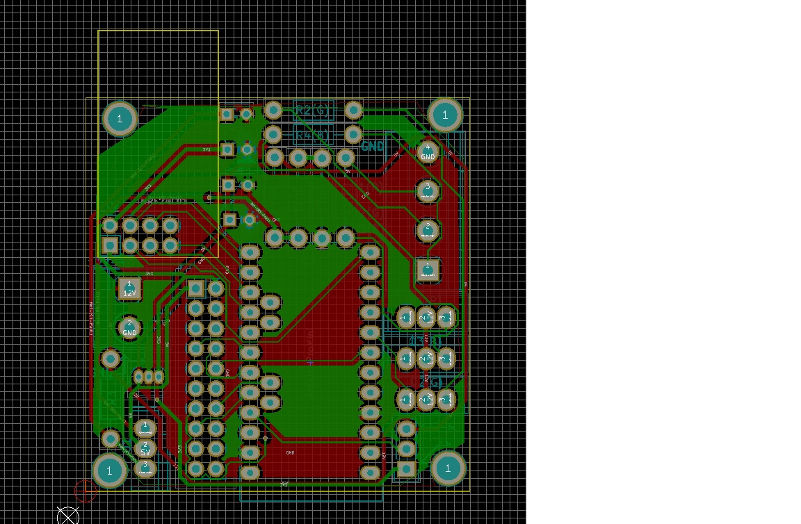
    So I created a "pour" on the front for GND plane and the PCB now looks like this:
    0_1466457414554_RGB-PCB.jpg

    What do I want to do on the back? Create another GND pour?

    -AM


  • Hardware Contributor

    Try out PCBWay, they're doing the first order for free. However you have to generate gerber files for them, in fact, to my knowledge OSHPark are one of very few to allow .brd files. I'm going to be doing a review for PCBWay soon on here, all i'm saying for now is they are fantastic service providers.

    Yes create a GND plane for the back too. I always have GND on front and back. I know some that have a VCC plane on one, but that depends on the components you use. Stick to GND on both to keep it simple.


  • Hardware Contributor

    yes.
    as you can see, it greatly simplify your old gnd routing. guess if you had started by doing this 😉
    and then, in future design, it would be possible to use vias if you need to fill some area where you can't have gnd because of other routing. same plane things for power etc... be careful, never put a gnd pour for AC lines, avoid when you can under antenna etc... there are some basics & advanced rules. but you will learn 🙂


  • @Samuel235 Thank you once again for all your help and feedback.

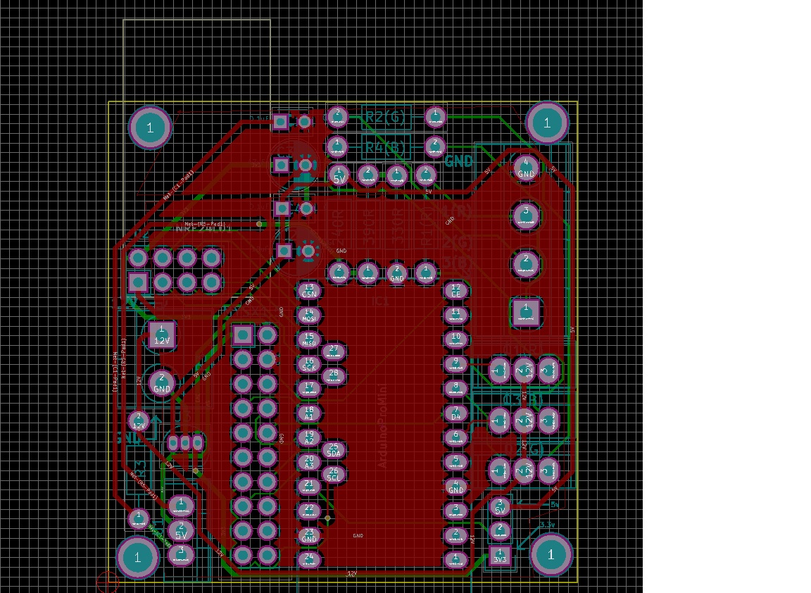
    Here is what it looks like after a GND pour on the back.

    I really want to add a OSH and Mysensors silkscreen on the front or back but I will have to learn how to do that. Am I getting too ambitious here 🙂

    -AM

    0_1466458431219_RGB-PCB.jpg


  • @scalz said:

    yes.
    as you can see, it greatly simplify your old gnd routing. guess if you had started by doing this 😉
    and then, in future design, it would be possible to use vias if you need to fill some area where you can't have gnd because of other routing. same plane things for power etc... be careful, never put a gnd pour for AC lines, avoid when you can under antenna etc... there are some basics & advanced rules. but you will learn 🙂

    I will have to read the above comment multiple times for it to sink through 🙂

    I tried to place NRF sticking out of the board so that there is no GND plane below the antenna. Do you see an issue in the PCB pic above with respect to antenna?

    -AM


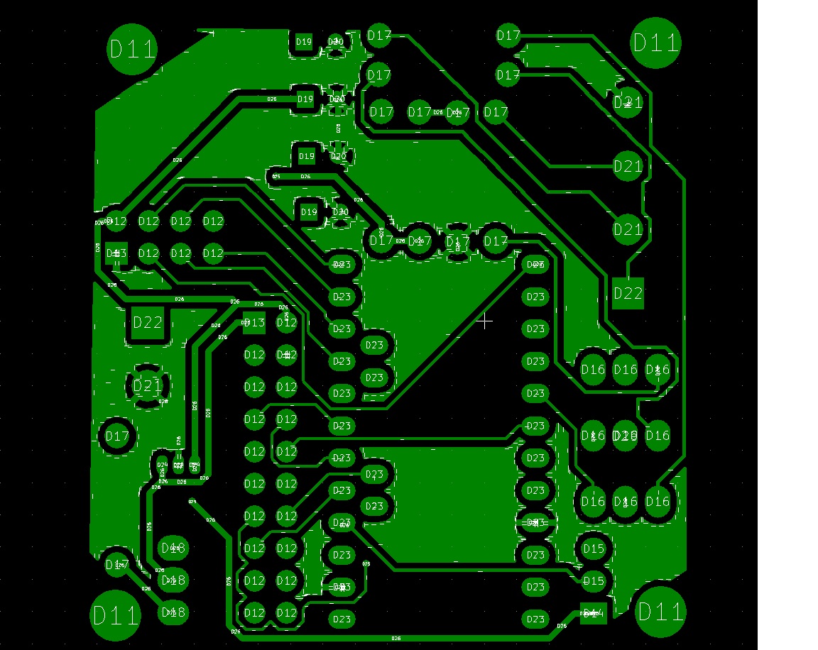
  • Here is what the gerber view looks like -

    Front Gerber:
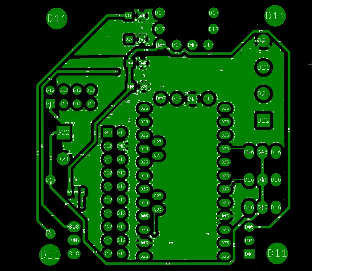
    0_1466459462138_RGB-front-gerber.jpg

    Back Gerber:

    0_1466459474210_RGB-back-gerber.jpg

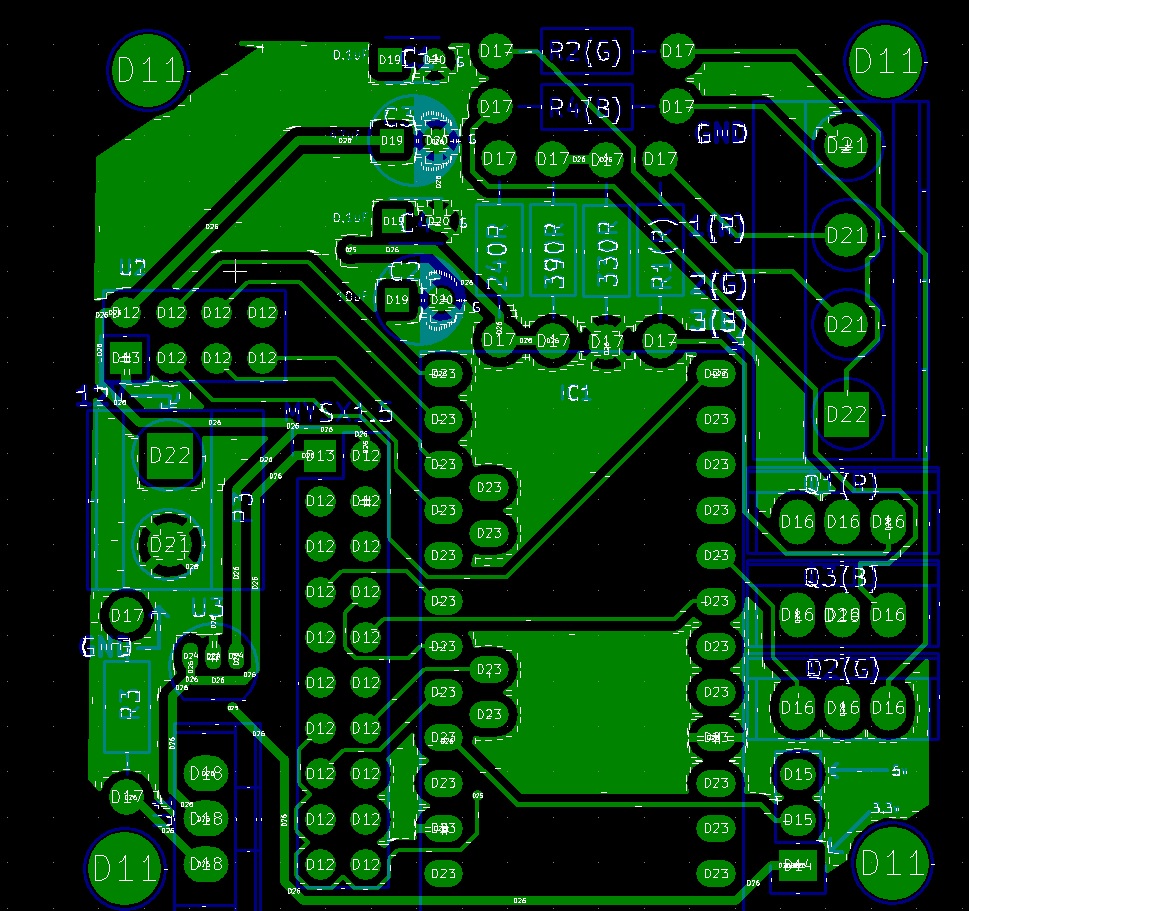
    Front Silkscreen:

    0_1466459509734_RGB-front-silkscreen.jpg

    Comments?

    -AM


  • Hardware Contributor

    @activemind, never too ambitious. Don't ever let anything stop you achieving what you want.

    The gerber files, i'm sure the front silkscreen shouldn't have any signs of the copper traces on. It should only be what you intend to see written/drawn on the surface of your board.


  • @Samuel235 Hmmmm, let me go back and see what went wrong with my silkscreen. My impression too was that it would show only the txt but when I file showed something different I put it up for review 🙂 Glad I did.

    Also, looking into OSH silkscreen!

    -AM


  • Looked at the silkscreen file and I had pulled up the wrong file in gerber view. Here is what the correct silkscreen looks like:
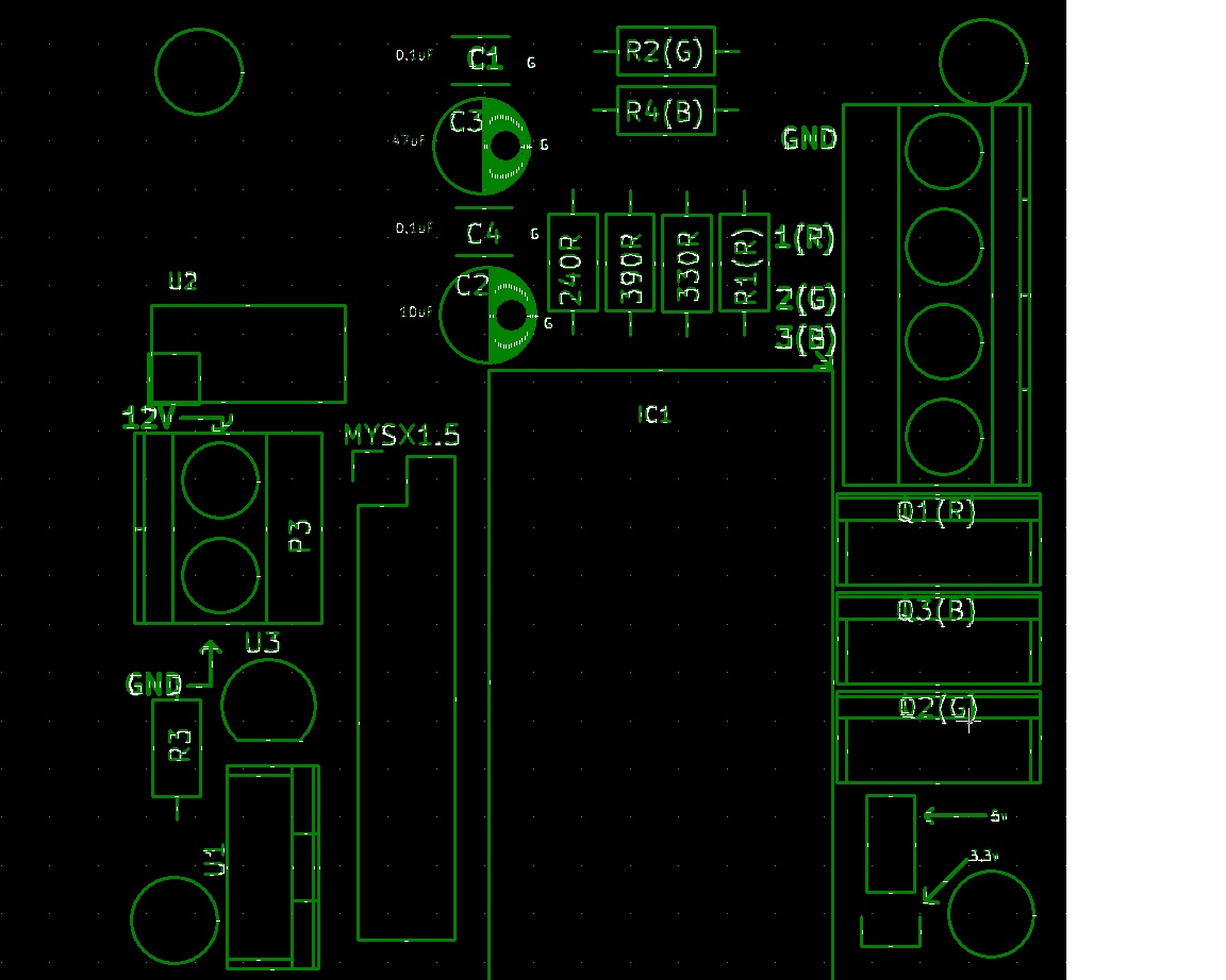
    0_1466462299596_RGB-front-silkscreen.jpg

    -AM


  • Done! Sent the files to Itead for processing 🙂

    Lets see if the boards work when they come back!

    Thanks for all your help @Samuel235 and @scalz

    -AM


  • managed to add the OSH and mysensors silkscreen I was thinking. Here is the final silkscreen...
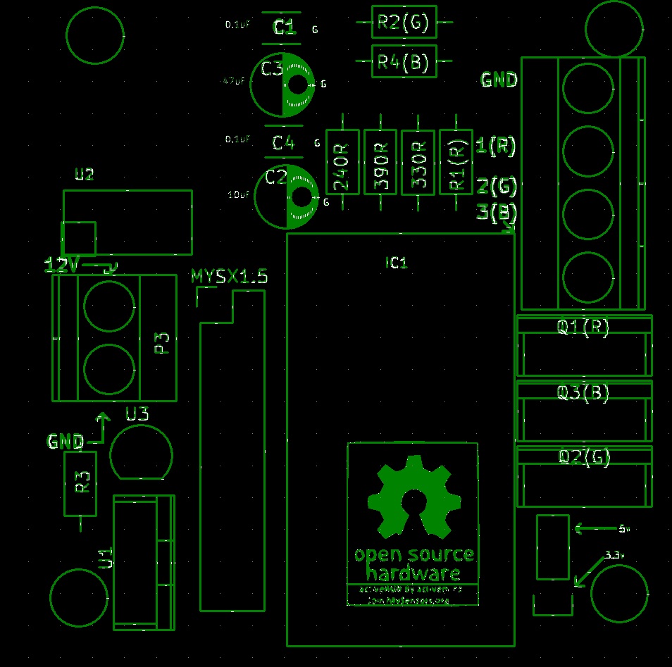
    0_1466475559476_RGB-front-silkscreen.jpg


  • Received an update from Itead. Everything looks good in gerber files. They have sent it to fab.

    Now the wait starts...

    -AM


  • Another update from Itead...PCBs complete and shipped!

    Cant wait to get my hands on my first PCB 🙂

    -AM


  • PCBs are in.... 🙂

    0_1467929726347_20160707_151923_resized.jpg
    0_1467929747083_20160707_151946_resized.jpg
    0_1467929773943_20160707_151958_resized.jpg

    Time to populate them now and see if they work 🙂

    -AM


  • Damn! Just realized some of my parts are still not in....

    Anyways, looking at the PCB,

    1. I think some of the text is just too small, like the cap values and OSH silkscreen. I need to make them bigger if I do a next rev.
    2. The mounting holes are a little too big. This is lightweight PCB and should not need heavyduty M3 screw. I could probably go with smaller mounting holes.
    3. Some silkscreen on the back would be nice...else it just looks naked 🙂

    -AM


  • i just found you project, looks pretty cool!
    did you manege to get it running?


  • @jeti Thank you. Unfortunately havent had a chance to assemble the boards yet. Have all the parts in but life gets in the way 🙂

    -AM


  • @activemind
    do you already have a BOM? and is there chance to help you out? I would be willing to assemble one or two of the boards :bowtie:


Log in to reply
 

Suggested Topics

  • 87
  • 8
  • 6
  • 1
  • 7
  • 7

49
Online

11.4k
Users

11.1k
Topics

112.7k
Posts