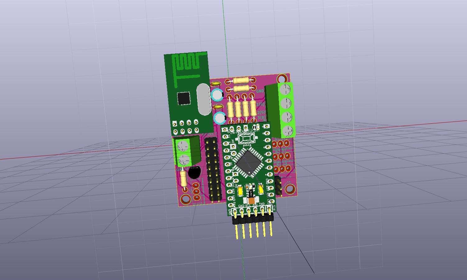
Yet Another RGB driver (activeRGB)
-
Just make sure your trace spacing conforms to that of the board house you are using. Board houses have minimum size and spacing rules, comply to those and you'll be good to go.
If there is no need to anchor it down, no terminals etc then you can get rid of it. However you have screw terminals there and then therefor i would advise to have a mount around that point. I normally attempt a M3 screw hole, which is around 3.5mm needed for the screw to pass through.
What is the size of your mounting holes now?
@Samuel235 said:
Just make sure your trace spacing conforms to that of the board house you are using. Board houses have minimum size and spacing rules, comply to those and you'll be good to go.
If there is no need to anchor it down, no terminals etc then you can get rid of it. However you have screw terminals there and then therefor i would advise to have a mount around that point. I normally attempt a M3 screw hole, which is around 3.5mm needed for the screw to pass through.
What is the size of your mounting holes now?
Hmmmm! The module I am using is called 1pin in KiCad and on measurement its around 4.5mm dia.
Am I making the holes too big? Let me see if there is some std module for 3.5mm holes.
-AM
-
@Samuel235 said:
Just make sure your trace spacing conforms to that of the board house you are using. Board houses have minimum size and spacing rules, comply to those and you'll be good to go.
If there is no need to anchor it down, no terminals etc then you can get rid of it. However you have screw terminals there and then therefor i would advise to have a mount around that point. I normally attempt a M3 screw hole, which is around 3.5mm needed for the screw to pass through.
What is the size of your mounting holes now?
Hmmmm! The module I am using is called 1pin in KiCad and on measurement its around 4.5mm dia.
Am I making the holes too big? Let me see if there is some std module for 3.5mm holes.
-AM
@activemind said:
@Samuel235 said:
Just make sure your trace spacing conforms to that of the board house you are using. Board houses have minimum size and spacing rules, comply to those and you'll be good to go.
If there is no need to anchor it down, no terminals etc then you can get rid of it. However you have screw terminals there and then therefor i would advise to have a mount around that point. I normally attempt a M3 screw hole, which is around 3.5mm needed for the screw to pass through.
What is the size of your mounting holes now?
Hmmmm! The module I am using is called 1pin in KiCad and on measurement its around 4.5mm dia.
Am I making the holes too big? Let me see if there is some std module for 3.5mm holes.
-AM
I take it back! I searched some more and found mounting hole 3.5mm footprint and it matches exactly what I have!Looks like I will have to move some stuff around to make some more space for the mounting holes :-(
-AM
-
Are M2 screw mounting holes okay or the standard is M3?
-AM
-
I would say the normal is M3 but honestly, use whatever you want to use. At the end of the day it is only a mounting screw. Not like its holding a lot of pressure. Go for an M2 hole if you want :) - Just keep any copper away from them for when you come to screw it down, you don't want to strip the silkscreen off and make a electrical connection to copper underneath :)
-
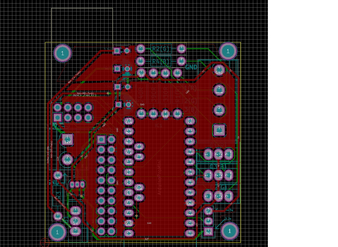
Moved around some routes and I was able to fit in M3 screw holes. I think this puppy is done now.
Whats the next step? What is all this copper filling?
-AM
-
Oh nice! What copper filling do you refer to?
-
The next step. I am looking at this tutorial and it talks about fill area and what not. I have no idea whats the next step.
Do I just generate the gerber files and I am done or there is some filling step reamining?
Still trying to wrap my head around this!
-AM
-
Your talking about GND planes. So, yeah you can do this, it isn't 100% necessary, but i do. Are you having issues following the guide to do it or are you asking me if you should do it?
-
I am asking if I should do it, keeping in mind that this is my first PCB and I want to keep it simple.
Based on what you said above, seems I can skip this step and just generate the gerber files and send them off to dirtyPCB. Is that right?
-AM
-
@activemind
i don't know how planes work in Kicad. but for multiple reasons, if I were you, I would add gnd plane. Try it, then you will know ;) Or don't try if you're not confident that should work too.
I won't do a lesson, there are lot of resources on internet, but mostly for :- impedance
- ground loop
- preventing noise and emi reduction
- etc.
plus when you start your board by drawing it where you need it, this ease your airwire then, at least in Eagle ;)
-
@scalz Thanks for your comment. ..means I need to read some more. I am not sure I completely understand the concept yet!
I tried uploading my kicad_brd file at OSHpark and it looks good, though I am not sure about solder mask.
I think I should not rush and read up on ground plane and soldermask before I submit the file for fab.
The nice part about OSH (even though its pricier than dirtyPCB) is that it takes pcb file directly so I dont have to deal with the various formats....or am I mistaken and the info is embedded in the file?
Let me go read more about GND planes and see what I need to do.
-AM
-
@scalz Thanks for your comment. ..means I need to read some more. I am not sure I completely understand the concept yet!
I tried uploading my kicad_brd file at OSHpark and it looks good, though I am not sure about solder mask.
I think I should not rush and read up on ground plane and soldermask before I submit the file for fab.
The nice part about OSH (even though its pricier than dirtyPCB) is that it takes pcb file directly so I dont have to deal with the various formats....or am I mistaken and the info is embedded in the file?
Let me go read more about GND planes and see what I need to do.
-AM
@activemind I can only agree with Scalz here, i would impliment it. And next board you do, implement it at the start, means less routes are required.
-
@Samuel235 Thanks for the advice. I will try to do it.
Also, what fab house would yuou recommend for 2-3 prototypes and then maybe I can shift it to dirtyPCB. OSHpark?
-AM
-
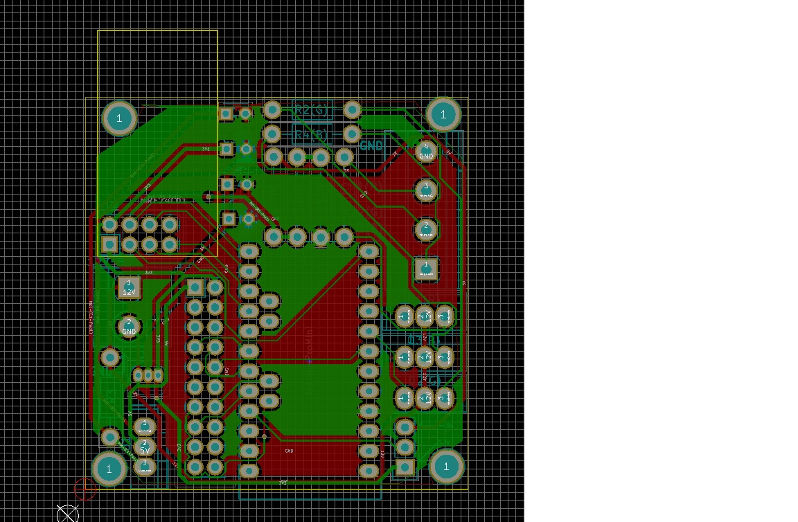
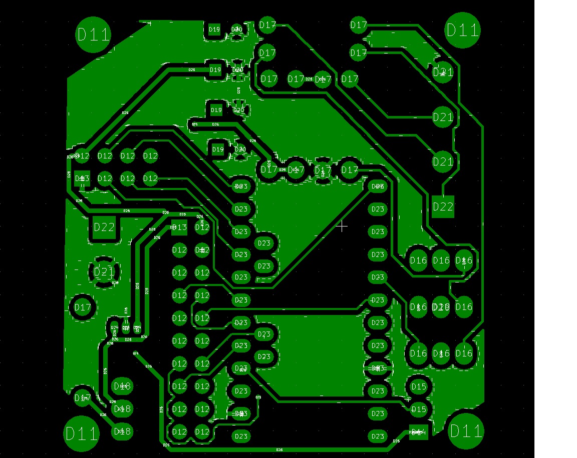
Reading some more and playing around with the tool I "think" I understand what its trying to do.
So I created a "pour" on the front for GND plane and the PCB now looks like this:
What do I want to do on the back? Create another GND pour?
-AM
-
Try out PCBWay, they're doing the first order for free. However you have to generate gerber files for them, in fact, to my knowledge OSHPark are one of very few to allow .brd files. I'm going to be doing a review for PCBWay soon on here, all i'm saying for now is they are fantastic service providers.
Yes create a GND plane for the back too. I always have GND on front and back. I know some that have a VCC plane on one, but that depends on the components you use. Stick to GND on both to keep it simple.
-
yes.
as you can see, it greatly simplify your old gnd routing. guess if you had started by doing this ;)
and then, in future design, it would be possible to use vias if you need to fill some area where you can't have gnd because of other routing. same plane things for power etc... be careful, never put a gnd pour for AC lines, avoid when you can under antenna etc... there are some basics & advanced rules. but you will learn :) -
@Samuel235 Thank you once again for all your help and feedback.
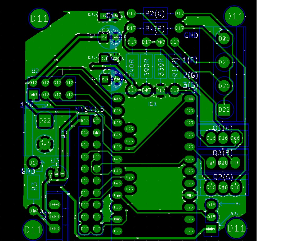
Here is what it looks like after a GND pour on the back.
I really want to add a OSH and Mysensors silkscreen on the front or back but I will have to learn how to do that. Am I getting too ambitious here :-)
-AM
-
yes.
as you can see, it greatly simplify your old gnd routing. guess if you had started by doing this ;)
and then, in future design, it would be possible to use vias if you need to fill some area where you can't have gnd because of other routing. same plane things for power etc... be careful, never put a gnd pour for AC lines, avoid when you can under antenna etc... there are some basics & advanced rules. but you will learn :)@scalz said:
yes.
as you can see, it greatly simplify your old gnd routing. guess if you had started by doing this ;)
and then, in future design, it would be possible to use vias if you need to fill some area where you can't have gnd because of other routing. same plane things for power etc... be careful, never put a gnd pour for AC lines, avoid when you can under antenna etc... there are some basics & advanced rules. but you will learn :)I will have to read the above comment multiple times for it to sink through :-)
I tried to place NRF sticking out of the board so that there is no GND plane below the antenna. Do you see an issue in the PCB pic above with respect to antenna?
-AM
-
Here is what the gerber view looks like -
Front Gerber:
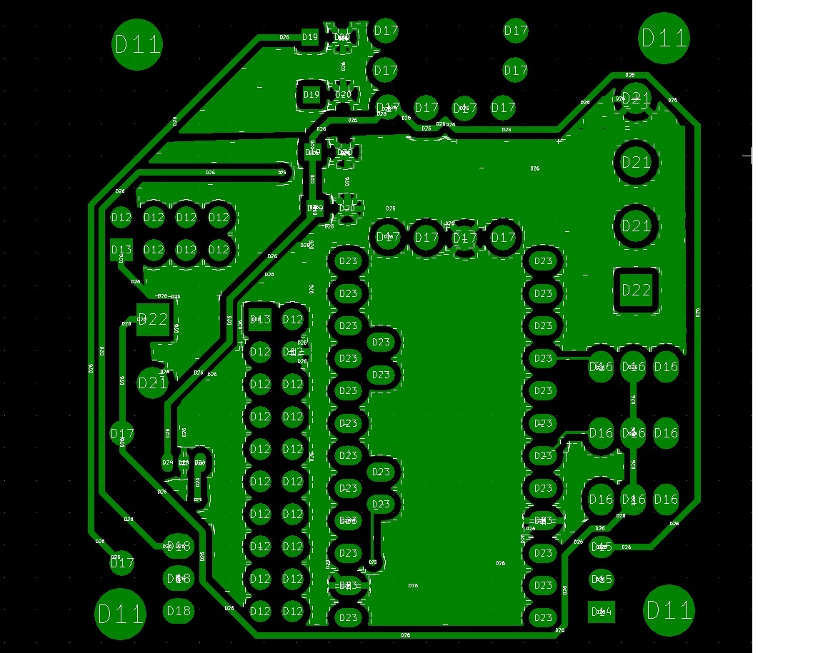
Back Gerber:
Front Silkscreen:
Comments?
-AM
-
Here is what the gerber view looks like -
Front Gerber:
Back Gerber:
Front Silkscreen:
Comments?
-AM
@activemind, never too ambitious. Don't ever let anything stop you achieving what you want.
The gerber files, i'm sure the front silkscreen shouldn't have any signs of the copper traces on. It should only be what you intend to see written/drawn on the surface of your board.
Hello! It looks like you're interested in this conversation, but you don't have an account yet.
Getting fed up of having to scroll through the same posts each visit? When you register for an account, you'll always come back to exactly where you were before, and choose to be notified of new replies (either via email, or push notification). You'll also be able to save bookmarks and upvote posts to show your appreciation to other community members.
With your input, this post could be even better 💗
Register Login