Yet Another RGB driver (activeRGB)
-
We could do with someone getting involved that has KiCad experience because i just have zero. I'm assuming that all those header pins and the different sized resistors are wrong too.
I'm not too sure why the arduino is actually shown on the board with separate serial header either. You only need 2 rows of female headers for your arduino to soxket in to.
I can only assume the libraries used here are incorrect on certain things.
@Samuel235 said:
We could do with someone getting involved that has KiCad experience because i just have zero. I'm assuming that all those header pins and the different sized resistors are wrong too.
I'm not too sure why the arduino is actually shown on the board with seperate serial header either. You only need 2 rows of female headers for your arduino to soxket in to.
The arduino footprint in from github. So I would assume that is correct!
I found the issue with resistor footprint. I had chosen 20mm for 3 and 10mm for the remaining ones. I think I want 10mm for all of them. Though R1,R2 & R4 need to higher wattage but I will deal with that detail after I have sorted out the size issue.
I also realized that I need to add connectors for 12V input power and 4 LED output signals!
Duh! :-)
-AM
-
@Samuel235 said:
We could do with someone getting involved that has KiCad experience because i just have zero. I'm assuming that all those header pins and the different sized resistors are wrong too.
I'm not too sure why the arduino is actually shown on the board with seperate serial header either. You only need 2 rows of female headers for your arduino to soxket in to.
The arduino footprint in from github. So I would assume that is correct!
I found the issue with resistor footprint. I had chosen 20mm for 3 and 10mm for the remaining ones. I think I want 10mm for all of them. Though R1,R2 & R4 need to higher wattage but I will deal with that detail after I have sorted out the size issue.
I also realized that I need to add connectors for 12V input power and 4 LED output signals!
Duh! :-)
-AM
@activemind, learning is the name of the game 😉
-
@activemind, learning is the name of the game 😉
@Samuel235 said:
@activemind, learning is the name of the game 😉
Very true! Once again, thanks much for active feedback! :-)
-AM
-
Looking better after I fixed the cap and resistor footprints...
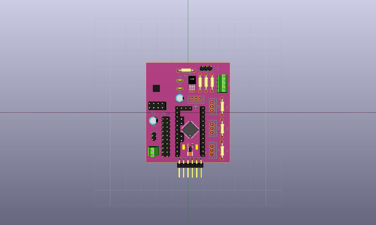
Do I need to be concerned about arduino footprints if I got them from mysensors github?
Need to add labels now and size the PCB?
-AM
-
Looking much neater and correct now. I wouldn't say you need to be doubting the footprints on github, but i still don't like the look of how KiCAD is showing this on the board. If that was in Eagle it would be showing that i need to solder each component of the arduino onto my board, not pushing a arduino into a socket. However, KiCAD may be completely different to the way it displays things though. Like i said before, we need someone with some KiCAD experience around here, i can't remember who uses it here :(
-
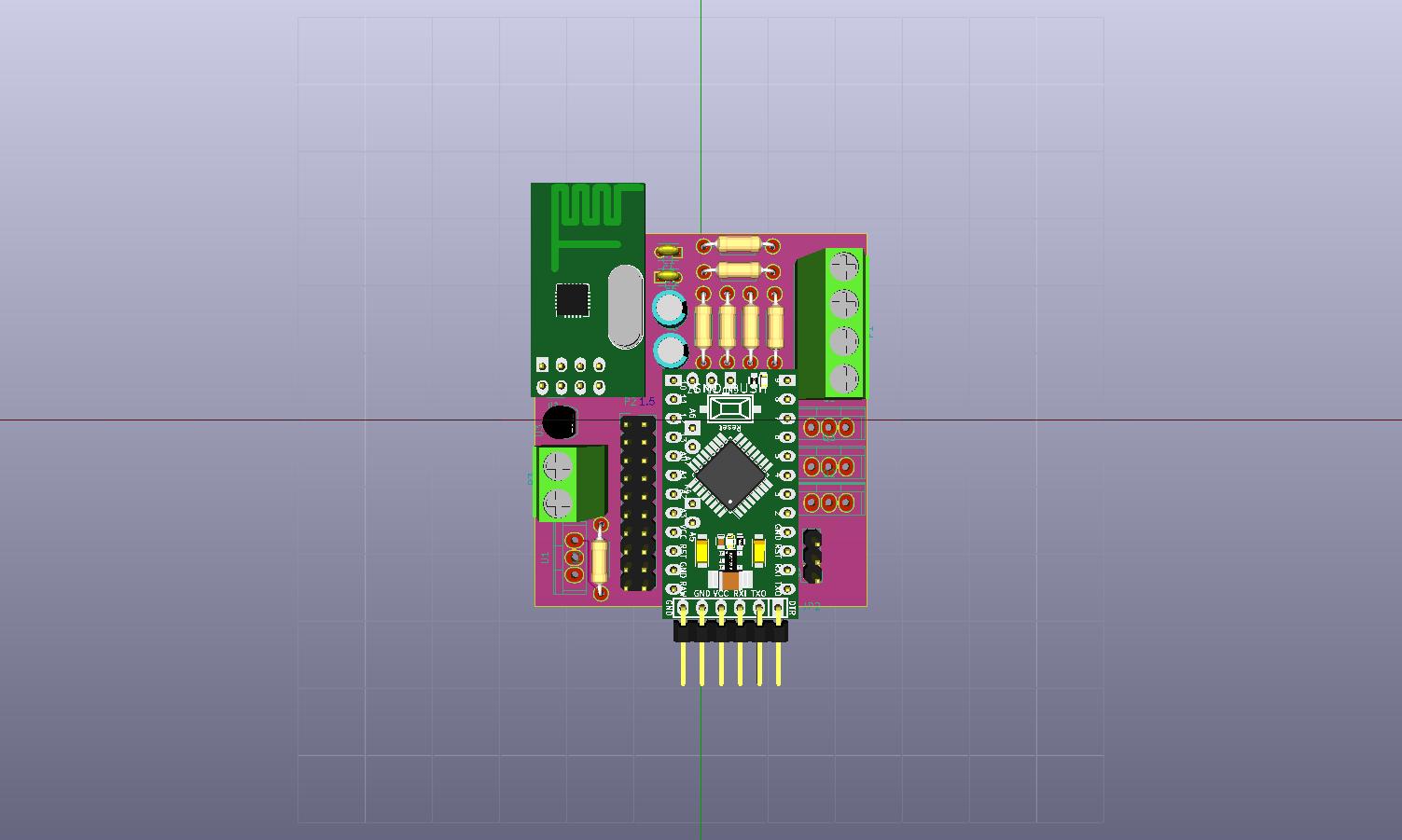
Played around with the placement a little more and I think I am happy with it now as this layout gives me space for silkscreen label and mounting holes.
I also got rid of the 2 pin jumper as it didnt really serve any purpose. Now LM317 always outputs 5V which is stepped down to 3.3V by LE33. Depending upon 3 jumper position you can use 3v3 or 5v pro mini. MySX header has both 5v and 3v3 so you can power the sensors off of that.
Trying to fix the github arduino pro model because I dont think its correct. There are 4 extra pins which are not there in the sparkfun model. Also, my 3D drawing does not have a different color compared to PCB. Need to fix those.
Anyways, here is the updated layout.
Once I cleanup all of the above and incorporate feedback (if any), I can start looking at routing the board :-) (which I have never done earlier).
-AM
-
Played around with the placement a little more and I think I am happy with it now as this layout gives me space for silkscreen label and mounting holes.
I also got rid of the 2 pin jumper as it didnt really serve any purpose. Now LM317 always outputs 5V which is stepped down to 3.3V by LE33. Depending upon 3 jumper position you can use 3v3 or 5v pro mini. MySX header has both 5v and 3v3 so you can power the sensors off of that.
Trying to fix the github arduino pro model because I dont think its correct. There are 4 extra pins which are not there in the sparkfun model. Also, my 3D drawing does not have a different color compared to PCB. Need to fix those.
Anyways, here is the updated layout.
Once I cleanup all of the above and incorporate feedback (if any), I can start looking at routing the board :-) (which I have never done earlier).
-AM
@activemind Looks a little better. Check the spacing between the MySX header and the side of where the arduino will sit, allow enough room for yourself there.
-
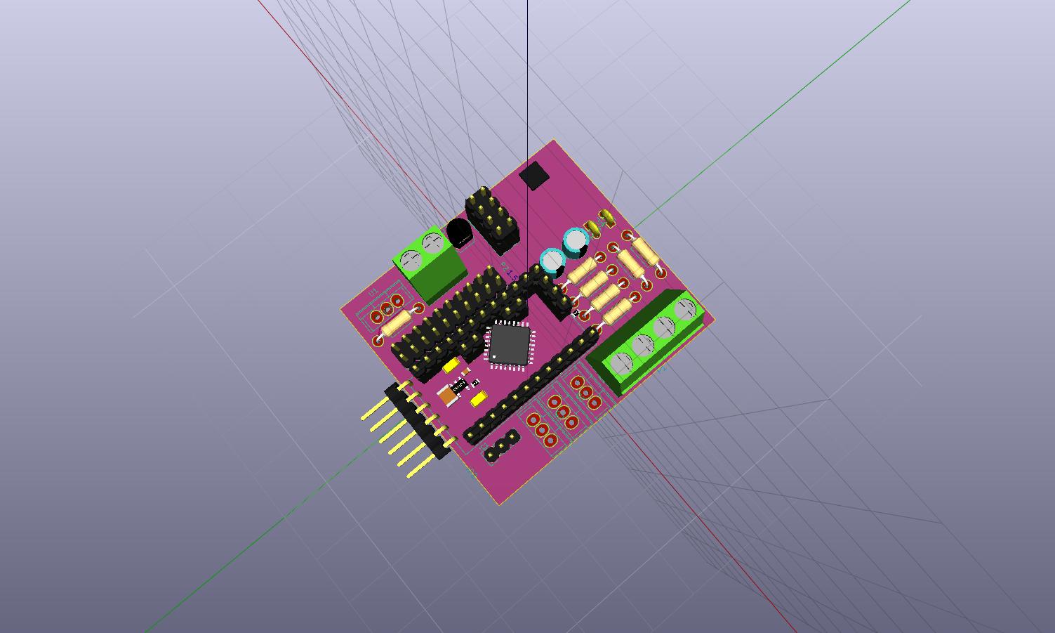
@Samuel235 Looks fine to my noob eyes :-)
Here is a view from a different angle (I also fixed my 3D model paths)
-AM
-
Now this looks more like what i would expect. Nice work dude, time to route it now ;)
-
@Samuel235 Thanks. Wouldnt have been possible to come this far without your help and feedback.
Going to try routing soon, I am thinking 10mil for normal trace and 80mil for 12v/5v/3v3/GND.
Does that sound right?
-AM
-
@Samuel235 Thanks. Wouldnt have been possible to come this far without your help and feedback.
Going to try routing soon, I am thinking 10mil for normal trace and 80mil for 12v/5v/3v3/GND.
Does that sound right?
-AM
@activemind said:
@Samuel235 Thanks. Wouldnt have been possible to come this far without your help and feedback.
Going to try routing soon, I am thinking 10mil for normal trace and 80mil for 12v/5v/3v3/GND.
Does that sound right?
-AM
80mil looks too fat :-)
How about 60mil?-AM
-
@activemind said:
@Samuel235 Thanks. Wouldnt have been possible to come this far without your help and feedback.
Going to try routing soon, I am thinking 10mil for normal trace and 80mil for 12v/5v/3v3/GND.
Does that sound right?
-AM
80mil looks too fat :-)
How about 60mil?-AM
Is it okay to route most of the power signal on the back and keep GND and everything else on the front?
General routing recommendations? (doing it for the first time :-)
-AM
-
Is it okay to route most of the power signal on the back and keep GND and everything else on the front?
General routing recommendations? (doing it for the first time :-)
-AM
@activemind, those traces are huge and i wouldn't go that big as it may cause imperfections in signal lines. You should be fine here with 10-12mil traces. If i remember correctly anyway.
I normally do ground planes/pours on top layer and bottom layer so all of the copper on the surfaces are ground unless its routed to a signal or vcc. However, keep it simple and just route it as you wish. There shouldn't be any issues here as its all relatively low voltage. If it makes it easier for yourself then yes, put all ground on the bottom.
-
Ok, I will go back to 12 mil for power and gnd and 10 mil for other signals.
-AM
-
Board is almost routed...
Just a couple of connections for MySX connector left.
Next step would be to silkscreen....no idea how to do that :-P
-AM
-
Found an issue! The footprint I had for LE33 was wrong! pins 1&3 were reversed!
Fixing and rerouting now..
-
Finding errors, creating the routes and the silkscreen are my favorite parts of module creation!
Learn to appreciate and enjoy these remaining steps as this is what you will be doing mostly when creating your own PCBs ;)
You're out of my depth now because everything remaining for you is software usage, and i do not have any experience with KiCAD unfortunately.
-
Thanks for all the feedback and holding my hand while trying to do this first PCB @Samuel235
It was fun routing the board with 20mil power(12v,5v,3.3v) & GND and 10 mil for rest of the signals.
But its done now.
Question: How big of a deal it is if I have 3 mounting holes rather than on all 4 corners? Or is it better if I make them smaller? Whats the std size everyone uses for mounting holes?
-
Here is what the PCB looks like after routing. Still some cleanup and checking to do but almost there...
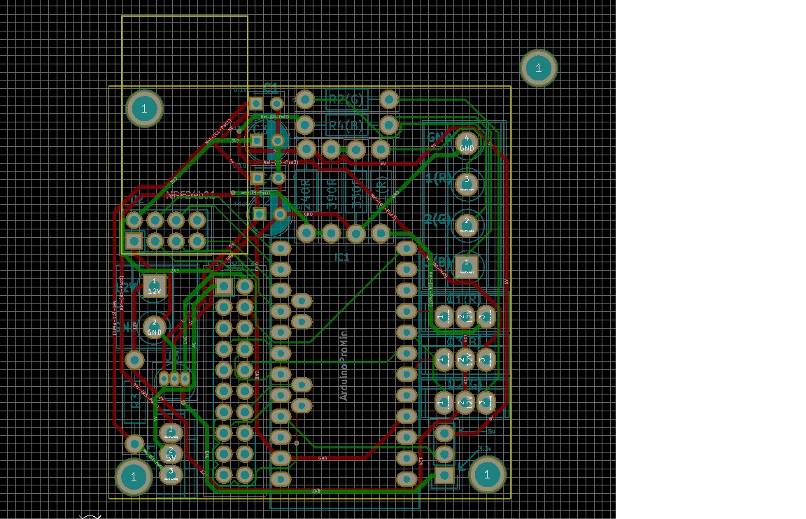
You can see that 4th mounting hole (right top) is outside the PCB. I had to move it temporarily so that I could route it. Now I need to make it smaller or drop it alltogether!
-AM