My Slim 2AA Battery Node
-
I also was about to order the 1.4 board. But are there any list of components that I need to complete the board?
@Cliff-Karlsson Sorry for late reply. I've not yet a BOM. I'll try o fix it later.
-
NEWS:
- A "final" version 2.0 redesigned i KiCad (very similar layout), panelized, ordered and tested OK.
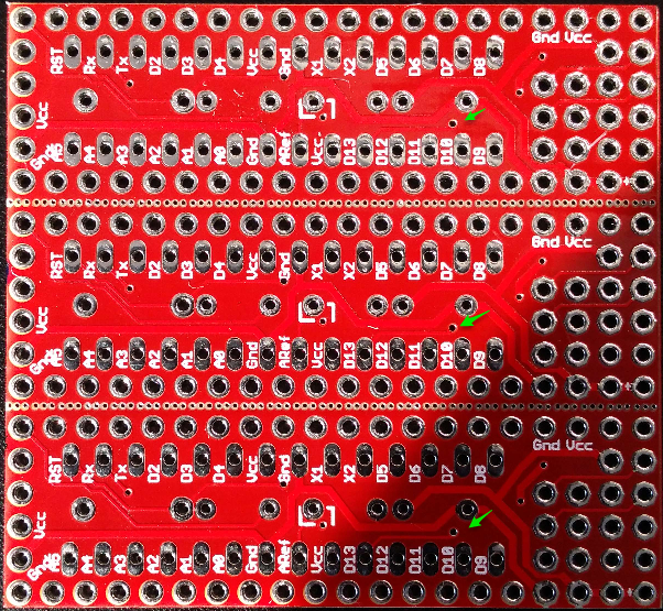
- A faulty via was introduced during panelization of v1.2, so the panelized v1.2 (blue board) needs a small fix to work.
More info ASAP.
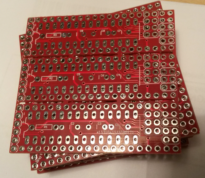
Edit 4/11: There seems to be no issues with v1.4 (red board) as I thought first. Luckily since it's now been shared a few times.
-
NEWS:
- A "final" version 2.0 redesigned i KiCad (very similar layout), panelized, ordered and tested OK.
- A faulty via was introduced during panelization of v1.2, so the panelized v1.2 (blue board) needs a small fix to work.
More info ASAP.
Edit 4/11: There seems to be no issues with v1.4 (red board) as I thought first. Luckily since it's now been shared a few times.
-
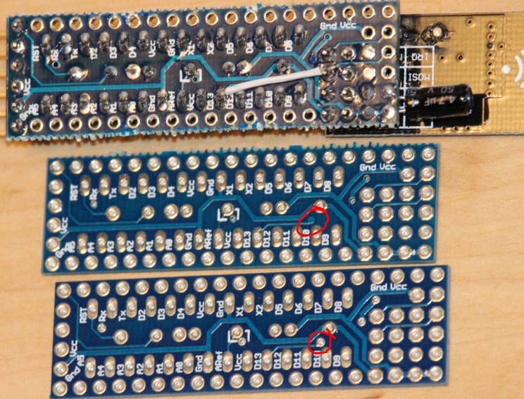
@AWI It should be easy the see the via with a missing hole. A connecting wire between Arduino D13 and nRF SCK is needed.
-
I've now tested v1.4 (red board) and it's working good in my MyS-net.
I can see that it has been shared 12 times at DirtyPCB, but don't know how I can see any money as suggested? As soon as I see any they'll be sent to MySensors.org.
Edit: Seems that I had a missing confirmation of my Paypal account. I'll try to solve this...
-
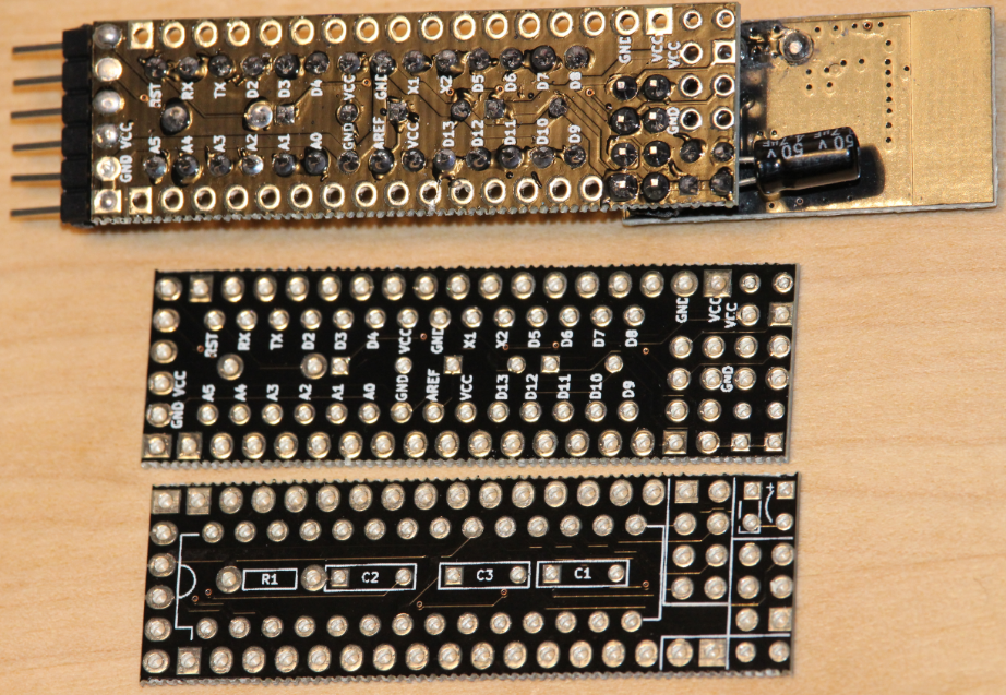
I decided to start learning KiCad instead of Eagle and that a tidy redesign of the Slim Node board would be a good start. Now when the red v1.4 board turned out to be quite ok (apart from the references R1,R2, R3, etc, as you can see above), I guess one can choose v1.4 or v2.0 by colour or by documentation. The v1.4 wasn't very well documented since I never really learned Eagle very good. I think that's improved now with v2.0. I've tested all the regular attributes (AVR ISP pins excluded) and it's OK.
This is my "final" version since I have a full stock of these boards for a while. If someone else want to pick up the design you're welcome.Here's all the KiCad files: MySlimNode2.0-kicad-design-doc.zip
Gerbers only in the panelized version folder.Here's a BOM (for v2.0): v2_BOM.txt
Purchase link to boardhouse (DirtyPCB). $1/order goes to MySensors.org like before.
This time it's black:
-
@m26872 Maybe you can add your info to this message (it's pinned):
http://forum.mysensors.org/topic/595/pcb-boards-for-mysensors -
I decided to start learning KiCad instead of Eagle and that a tidy redesign of the Slim Node board would be a good start. Now when the red v1.4 board turned out to be quite ok (apart from the references R1,R2, R3, etc, as you can see above), I guess one can choose v1.4 or v2.0 by colour or by documentation. The v1.4 wasn't very well documented since I never really learned Eagle very good. I think that's improved now with v2.0. I've tested all the regular attributes (AVR ISP pins excluded) and it's OK.
This is my "final" version since I have a full stock of these boards for a while. If someone else want to pick up the design you're welcome.Here's all the KiCad files: MySlimNode2.0-kicad-design-doc.zip
Gerbers only in the panelized version folder.Here's a BOM (for v2.0): v2_BOM.txt
Purchase link to boardhouse (DirtyPCB). $1/order goes to MySensors.org like before.
This time it's black:
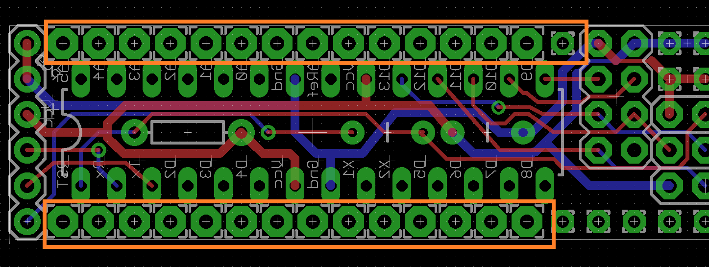
@m26872 There is something that I really can't understand.
Are the pin headers at the borders not connected to the IC pins ?
-
@m26872 There is something that I really can't understand.
Are the pin headers at the borders not connected to the IC pins ?
@ahmedadelhosni That's an important feature of this board design and one of the major diffenreces from e.g. Arduino Pro Mini. The rows of unconnected pins is like a prototyping area to mount sensors and/or other supporting components. It's easy to just fold the legs at bottom side and solder to the IC pins you want to connect to. I think you can see an example in the photos of a completed node in the first post above.
I've sized the pads so pin headers can be used there instead if desired, but then you have to connect every pin manually so that's not the primary purpose. The "Slim Node" was not just board project, but I've understood that many people enjoyed the board as a generic one, which is great.
-
@ahmedadelhosni That's an important feature of this board design and one of the major diffenreces from e.g. Arduino Pro Mini. The rows of unconnected pins is like a prototyping area to mount sensors and/or other supporting components. It's easy to just fold the legs at bottom side and solder to the IC pins you want to connect to. I think you can see an example in the photos of a completed node in the first post above.
I've sized the pads so pin headers can be used there instead if desired, but then you have to connect every pin manually so that's not the primary purpose. The "Slim Node" was not just board project, but I've understood that many people enjoyed the board as a generic one, which is great.
@m26872 great idea indeed. You convinced me :)
Did you think of monitoring the voltage as this type of nodes needs this or did you leave it also as an option for us ?
-
@m26872 great idea indeed. You convinced me :)
Did you think of monitoring the voltage as this type of nodes needs this or did you leave it also as an option for us ?
@ahmedadelhosni you don't need additional hardware to monitor the voltage. Look for the "vcc" library. It uses the internal reference.
-
@m26872 great idea indeed. You convinced me :)
Did you think of monitoring the voltage as this type of nodes needs this or did you leave it also as an option for us ?
@ahmedadelhosni
... or here. -
I received my panelized boards as well (guess 1.4). They look great!!.
I do have a question about this. Maybe it was just some silly thinking. I was trying to program the arduino 328p-pu on a regular arduino uno board (default motion sketch). After I did this I hooked it up on to the board.
However I am not receiving anything on the arduino serial monitor. I connected the arduino uno to your board. v to v, rx to rx, tx to tx, ground to ground and reset to reset. Am I just thinking to simple? Can someone please advise me to get this board up and running? I also soldered d13 additional to the nrf.
I soldered all caps, however I did not solder the resistor, is that one mandatory?
Many thanks and keep up the good work.
-
@ahmedadelhosni
... or here. -
I received my panelized boards as well (guess 1.4). They look great!!.
I do have a question about this. Maybe it was just some silly thinking. I was trying to program the arduino 328p-pu on a regular arduino uno board (default motion sketch). After I did this I hooked it up on to the board.
However I am not receiving anything on the arduino serial monitor. I connected the arduino uno to your board. v to v, rx to rx, tx to tx, ground to ground and reset to reset. Am I just thinking to simple? Can someone please advise me to get this board up and running? I also soldered d13 additional to the nrf.
I soldered all caps, however I did not solder the resistor, is that one mandatory?
Many thanks and keep up the good work.
@betonishard
If you've got red boards it's v1.4 and should not need the D13 fix. And R1 and C2 are mandatory if you want the 6 pin serial Arduino interface to work.Did you read about the necessary bootloader and fuse settings in the first post? An Atmega328p setup as standard Arduino wont work, because of Internal clock, BOD, etc. Perhaps Arduino Uno as a bootloader is good for you.
If you haven't any experience in bootloader and fuse settings, you should know that it can be a mess. A lot of things can go wrong. Nobody can walk you through it here. Look among all the existing toturials on the internet to find what is working for you and of course ask if you have any more specific questions.
-
I know I have many questions :) but how about inverting the nrf position by 180 degree so that it can be on top of the atmega and decrease that length. Would it fit in your design ?
Can you do such board for those who are interested like me :) ? -
I know I have many questions :) but how about inverting the nrf position by 180 degree so that it can be on top of the atmega and decrease that length. Would it fit in your design ?
Can you do such board for those who are interested like me :) ?@ahmedadelhosni
I think it's a good idea! And an easy mod, but it's not on priority list atm. Someone else would get a quick start from my already published kicad-files.The thought behind present design is that I didn't want anything to cover the antenna in any direction, but I doubt it would matter much in this suggested case. It'll be worse when it comes to the hight. Look at the photos. The nRF becomes too high for my enclosures if I use a socket, and the 328p with its socket is too high to fit under a nRF without its socket. The solution would be to remove the 328p socket and move the R and Cs to bottom side or somewhere else. And without a 328p socket, the 3x2 AVR ISP pins would become more important to keep. Otherwise the board could have been trimmed even more.
-
@ahmedadelhosni
I think it's a good idea! And an easy mod, but it's not on priority list atm. Someone else would get a quick start from my already published kicad-files.The thought behind present design is that I didn't want anything to cover the antenna in any direction, but I doubt it would matter much in this suggested case. It'll be worse when it comes to the hight. Look at the photos. The nRF becomes too high for my enclosures if I use a socket, and the 328p with its socket is too high to fit under a nRF without its socket. The solution would be to remove the 328p socket and move the R and Cs to bottom side or somewhere else. And without a 328p socket, the 3x2 AVR ISP pins would become more important to keep. Otherwise the board could have been trimmed even more.
@m26872 I guess the nrf above the atmega won't cause problems or interference to the atmega due to rf signals. so that's fine.
I measured the nrf and it will be 13 mm, so I thought it may fit as from the photos, I guess the max height can be 13 or 14. For me increasing the height is not a problem as I am still searching for cheap compact and not so long enclosure with maximum heigh 20 mm to use. I am searching for cheap products which are kept in that size of enclosure which I need but didn't find it yet :)
I didn't use Kicad before and I guess there is no converters to eagle. Youtube time :)
Can you please tell me the total length of the board + nrf ?
Hello! It looks like you're interested in this conversation, but you don't have an account yet.
Getting fed up of having to scroll through the same posts each visit? When you register for an account, you'll always come back to exactly where you were before, and choose to be notified of new replies (either via email, or push notification). You'll also be able to save bookmarks and upvote posts to show your appreciation to other community members.
With your input, this post could be even better 💗
Register Login