12V distribution box - mysensorized!
-
I need some help from one of the hw guys.
I have arduino pin driving the gate of a FET like so many other examples.
I have another signal called Fault which is active low.
Now I want to and the two signals such that when fault becomes active (becomes 0), the FET is forced off.
Whats the circuit for that?
Thanks
-AM@activemind said:
I need some help from one of the hw guys.
I have arduino PWM pin driving the gate of a FET like so many other examples.
I have another signal called Fault which is active low.
Now I want to and the two signals such that when fault becomes active (becomes 0), the FET is forced off.
Whats the circuit for that?
Thanks
-AM -
Nevermind, found the answer. Just put another FET in there with fault signal driving the gate.
-AM
-
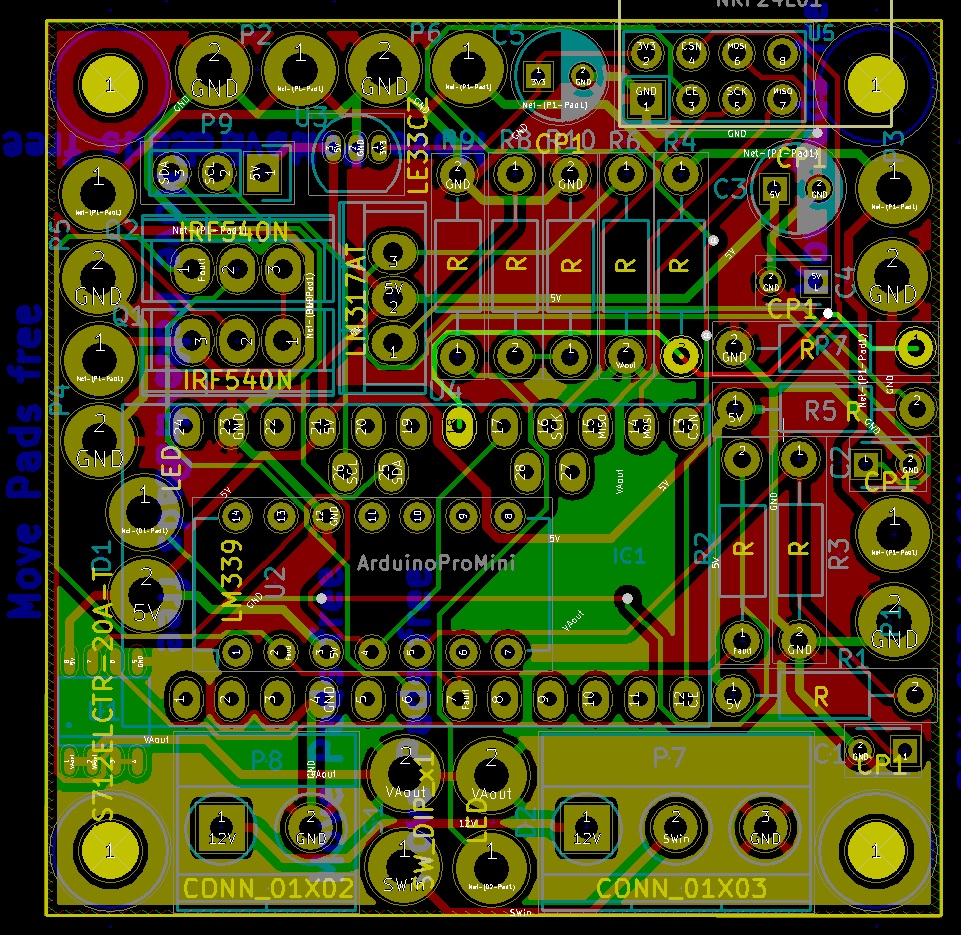
So I managed to finish the schematic and and posting it for people to look over.
Features:- 1 input and 6 output - 12V
- Easy hook ups for Voltmeter/Ammeter display.
- Voltage and current draw fed back to arduino as input.
- Hardware based overcurrent protection with latch feature.
- Fault status can be reported back to Controller.
- Switch to turn supply off.
- LED indicators for power on and fault.
- All easy solder through components.
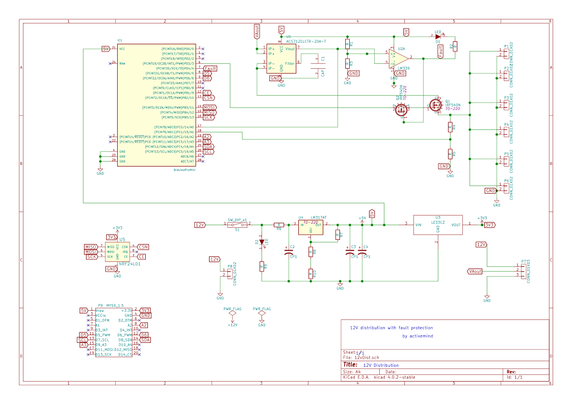
Comments?
-AM
-
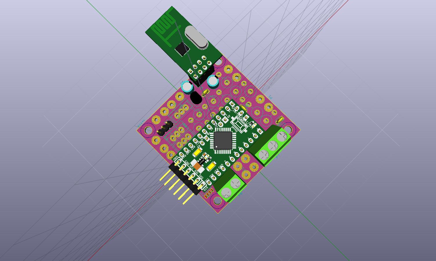
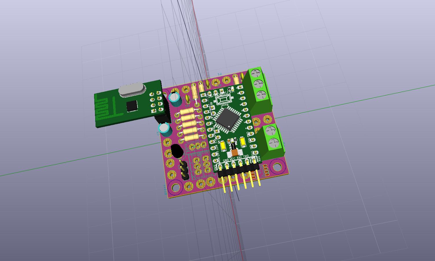
Initial placement is done and this is what it looks like....very crowded board. Had to place the comparator underneath the pro mini, is that going to be an issue?
-
Also, thinking ahead about routing this board. Is it okay to do a GND pour on one side and 12V on the other?
-AM
-
redid some of the placement and changed the resistors to horizontal mount from vertical.
looking better...I guess :-)
-AM
-
Debating about changing the size to 5x9 size so that it can fit inside a 5x10 box like this
-AM
-
@activemind those boxes are 56x95mm on the inside (I have lots of them). They have mounting points in the corners, about 1.5mm from the inner wall. The outer diameter of the mounting points is 5.5mm and the inner diameter is approximately 2mm.
-
A little off topic, but what PCB software are you using to do your illustrations and layout? It looks like nice software. Is it for windows only or is there a linux version?
@dbemowsk said:
A little off topic, but what PCB software are you using to do your illustrations and layout? It looks like nice software. Is it for windows only or is there a linux version?
I am a KiCad beginner. I started like a couple of days ago and this is my second PCB. Waiting for the first one to come back from fab house :-)
-AM
-
@activemind those boxes are 56x95mm on the inside (I have lots of them). They have mounting points in the corners, about 1.5mm from the inner wall. The outer diameter of the mounting points is 5.5mm and the inner diameter is approximately 2mm.
@mfalkvidd said:
@activemind those boxes are 56x95mm on the inside (I have lots of them). They have mounting points in the corners, about 1.5mm from the inner wall. The outer diameter of the mounting points is 5.5mm and the inner diameter is approximately 2mm.
Thanks for the measurements @mfalkvidd . I am still debating about increasing the PCB size though because I looked at one of my existing boxes with the DC connector I am planning to use, and I realized that I need little more space because the connector extend out.
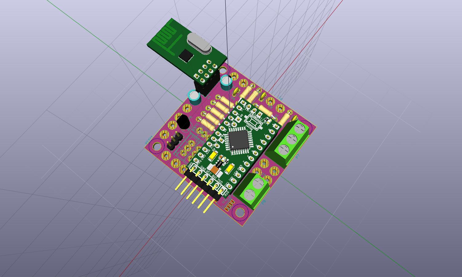
Still playing with the placement on the PCB but looks like I have everything in place for now. Lets see what happens when I try to route it!
The only thing I am concerned about is will placing the comparator IC underneath the pro mini cause any issues?
-AM
-
@mfalkvidd said:
@activemind those boxes are 56x95mm on the inside (I have lots of them). They have mounting points in the corners, about 1.5mm from the inner wall. The outer diameter of the mounting points is 5.5mm and the inner diameter is approximately 2mm.
Thanks for the measurements @mfalkvidd . I am still debating about increasing the PCB size though because I looked at one of my existing boxes with the DC connector I am planning to use, and I realized that I need little more space because the connector extend out.
Still playing with the placement on the PCB but looks like I have everything in place for now. Lets see what happens when I try to route it!
The only thing I am concerned about is will placing the comparator IC underneath the pro mini cause any issues?
-AM
The only thing I am concerned about is will placing the comparator IC underneath the pro mini cause any issues?
As long as the Pro Mini is placed high enouch to not touch the IC it won't cause any issues. The jmodule uses the same idea: https://www.openhardware.io/view/20/jModule
-
Thanks @mfalkvidd for the link. I feel more confident that this might work.
Didnt get a chance to work on this for past couple of days. Maybe soon...
-AM
-
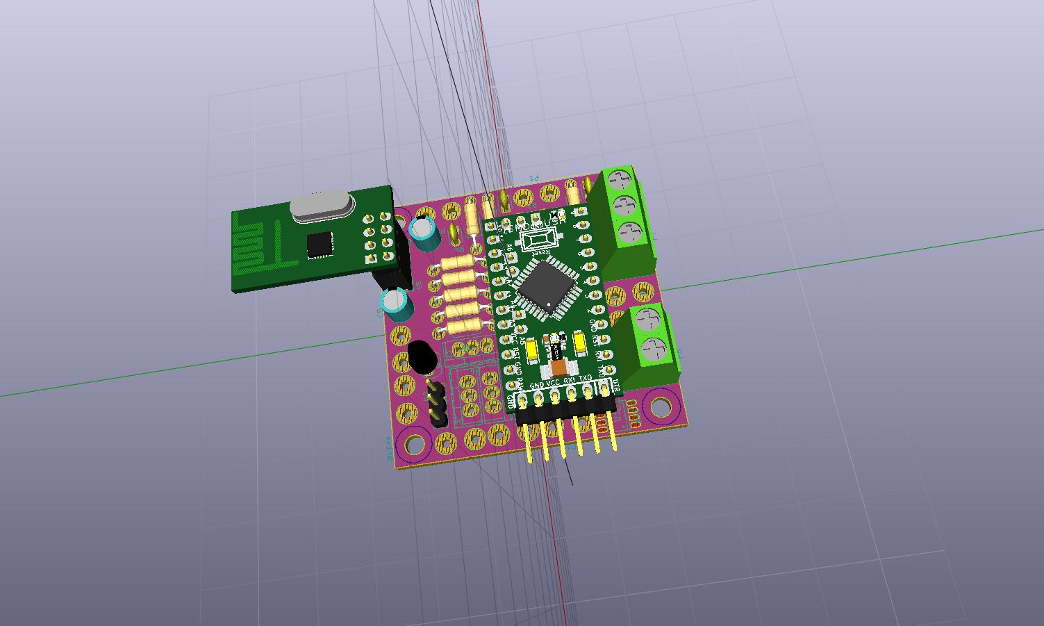
Ok, so the board is routed. This was fun....very crowded board...at least by my noob standards :-)
Done all DRC and connectivity checks...looks good.
-AM
-
-
Just a quick thought, but would it be preferable to attach something like this to the PCB using connections for current measurement rather than the ACS chip?
Modules have the benefit of being optional, so you can skip them if you don't want them on a certain channel. In other words, it is conceivable to have 4 out of 5 channels that report and 1 that doesn't, for example.
Because the cost of the module and chip are same, I don't believe there is any difference from a financial standpoint.
-AM
Hello! It looks like you're interested in this conversation, but you don't have an account yet.
Getting fed up of having to scroll through the same posts each visit? When you register for an account, you'll always come back to exactly where you were before, and choose to be notified of new replies (either via email, or push notification). You'll also be able to save bookmarks and upvote posts to show your appreciation to other community members.
With your input, this post could be even better 💗
Register Login