-
[edit] Discussion about alignment of MYSX connector forked from here:
https://forum.mysensors.org/topic/2740/easy-newbie-pcb-for-mysensors/521Ok thank you @Anticimex for the explanation, I misunderstood (mixed up edges of the board and edges of the connector in the sentence) and thought the connector should be spaced 100mil away from the board edge.
Sorry @sundberg84 :)
@Anticimex to explain more: without knowing the distance to at least one of the edges, it's not really possible to make a daughter board with a reed switch or hall sensor that will work on any motherboard. I guess it's the only case where it's annoying but for that case it is :)
@nca78 @sundberg84 In general, I would recommend placing the connector and align the courtyard along the edge.
That way, you will get a standard 100mil spacing to the long edge of the connector. It is tricky to put requirement on a second edge due to the pin1 orientation requirement since that essentially require all motherboards to place MYSX at the top left.
It of course helps alignment-sensitive daughterboards such as yours to ensure motherboard edge alignment, but it puts great restrictions on motherboards. It is a tricky balance.I'd suggest you fight it out and then we update the spec if needed ;)
I can see the merit of both alternatives.
-
[edit] Discussion about alignment of MYSX connector forked from here:
https://forum.mysensors.org/topic/2740/easy-newbie-pcb-for-mysensors/521Ok thank you @Anticimex for the explanation, I misunderstood (mixed up edges of the board and edges of the connector in the sentence) and thought the connector should be spaced 100mil away from the board edge.
Sorry @sundberg84 :)
@Anticimex to explain more: without knowing the distance to at least one of the edges, it's not really possible to make a daughter board with a reed switch or hall sensor that will work on any motherboard. I guess it's the only case where it's annoying but for that case it is :)
@nca78 - no worries, and as I said - I had the same questions.
@Anticimex - I understand your concerns and the balance but not to specify top-left means that you can only make daughtherboards as long as the connector or the daughtherboard have a risk of be aligned under the motherboard.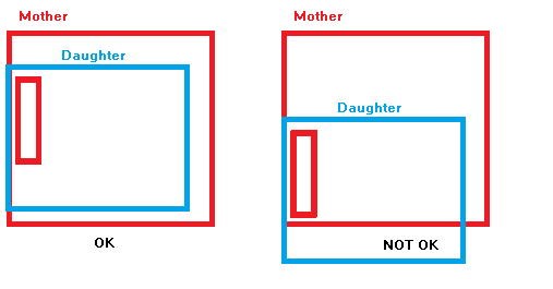
If we could specify top-left, it doesnt mean the connector is stuck in one corner. You could rotate this 90dgr meaning you have all four corners to work with.
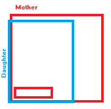
In my case I aligned it in the bottom-left corner. Same there... possible to rotate it but that can cause issues with differente MysX version (length of the connector).
@mfalkvidd - could we move this MysX discussion to the MysX thread intstead? Or Maybe anticimex can fix that?
-
@nca78 - no worries, and as I said - I had the same questions.
@Anticimex - I understand your concerns and the balance but not to specify top-left means that you can only make daughtherboards as long as the connector or the daughtherboard have a risk of be aligned under the motherboard.If we could specify top-left, it doesnt mean the connector is stuck in one corner. You could rotate this 90dgr meaning you have all four corners to work with.
In my case I aligned it in the bottom-left corner. Same there... possible to rotate it but that can cause issues with differente MysX version (length of the connector).
@mfalkvidd - could we move this MysX discussion to the MysX thread intstead? Or Maybe anticimex can fix that?
@sundberg84 A valid point. Still it is more restricted than currently, but I have no problem with it, and if you are fine with it, lets go for that. I will update the spec to clarify that pin1 should be oriented to be closest to the corner of the board, with 100mil spacing to both edges.
-
@sundberg84 A valid point. Still it is more restricted than currently, but I have no problem with it, and if you are fine with it, lets go for that. I will update the spec to clarify that pin1 should be oriented to be closest to the corner of the board, with 100mil spacing to both edges.
@anticimex - I understand your points as well - and i think you should hold on until others in the community can share their thoughs as well. I dont want to be the only one changing this - it might be to the worse.
-
@nca78 - no worries, and as I said - I had the same questions.
@Anticimex - I understand your concerns and the balance but not to specify top-left means that you can only make daughtherboards as long as the connector or the daughtherboard have a risk of be aligned under the motherboard.If we could specify top-left, it doesnt mean the connector is stuck in one corner. You could rotate this 90dgr meaning you have all four corners to work with.
In my case I aligned it in the bottom-left corner. Same there... possible to rotate it but that can cause issues with differente MysX version (length of the connector).
@mfalkvidd - could we move this MysX discussion to the MysX thread intstead? Or Maybe anticimex can fix that?
@sundberg84 As for issue of the length of the connector, no, it should not be a problem. It always start with pin1 and grows "downward". As long as pin1 is closest to the corner, any MYSX version should align, as long as they can physically fit.
-
@sundberg84 As for issue of the length of the connector, no, it should not be a problem. It always start with pin1 and grows "downward". As long as pin1 is closest to the corner, any MYSX version should align, as long as they can physically fit.
@anticimex -exactly! But it will not work if you did like I did it in EasyPCB and start from the last pin :) (Bottom-left)
-
@anticimex -exactly! But it will not work if you did like I did it in EasyPCB and start from the last pin :) (Bottom-left)
@sundberg84 No, but that is just the price of evolution.
-
@sundberg84 No, but that is just the price of evolution.
@anticimex - happy to pay that price, isnt that what open hardware is all about? Stronger together...
-
@anticimex - happy to pay that price, isnt that what open hardware is all about? Stronger together...
@sundberg84 I will just go ahead and update the spec. Yes, it may cause some existing designs to violate the spec, but that will always be the case. We look forwards, not backwards :)
Spec is here. -
@sundberg84 I will just go ahead and update the spec. Yes, it may cause some existing designs to violate the spec, but that will always be the case. We look forwards, not backwards :)
Spec is here.@anticimex @Nca78
What would you say is the clearance needed for components above a motherboard? If we wants a daugtherboard to be "on-top" with only a 2,54 male header on the motherboard (should this be soldered to the daugherboard?) we are talking about 2-3mm clearance and with this... not many through-hole components will fit.Another way would be not to specify how the daugher and mother should be connected. In EasyPCB I have all the components on top... and I should without issues be able to solder a single 2.54 male header between these boards if the daugherboard connected under the motherboard. This is actually my plan... because to be able to follow the rules + clearance I have to solder male header onto the mother and a female header onto the daugher.
-
@anticimex @Nca78
What would you say is the clearance needed for components above a motherboard? If we wants a daugtherboard to be "on-top" with only a 2,54 male header on the motherboard (should this be soldered to the daugherboard?) we are talking about 2-3mm clearance and with this... not many through-hole components will fit.Another way would be not to specify how the daugher and mother should be connected. In EasyPCB I have all the components on top... and I should without issues be able to solder a single 2.54 male header between these boards if the daugherboard connected under the motherboard. This is actually my plan... because to be able to follow the rules + clearance I have to solder male header onto the mother and a female header onto the daugher.
@sundberg84 quoting the spec:
The motherboard provides the male part and the daughterboard mates using the corresponding female part.So clearance should be based on the male socket that the pins go through in the header. But we could add a few mm so the motherboard is able to place low profile parts underneath, while restricting daughterboards to only use low profile parts on the back side.
-
in the same time, it doesnt say if the motherboard should be on top or bottom :)
I want to be able to use a daugherboard as big as the motherboard (50x50) so I think the clearance needs to be atleast so you can fit a nrf24l01+.daughterboard mates using the corresponding female part.
This is possible if the daugherboard uses the female 2.54 pins.
@sundberg84 correct, the spec allows you to place the connector on either side. And right now, it is permissive of component placement and only give recommendations.
-
@sundberg84 correct, the spec allows you to place the connector on either side. And right now, it is permissive of component placement and only give recommendations.
@anticimex ok, sounds good! That makes two possibilities for any user. If a user for example wants to use female + male header on radio + pro mini on EasyPCB they will not be able to use a daugherboard on top... but can connect it under.
and to save space im going to use single male headers and solder them to both boards.
-
@anticimex ok, sounds good! That makes two possibilities for any user. If a user for example wants to use female + male header on radio + pro mini on EasyPCB they will not be able to use a daugherboard on top... but can connect it under.
and to save space im going to use single male headers and solder them to both boards.
@sundberg84 just be careful if having a design that encourage mounting the MYSX on both sides. Since a daughterboard will have to do the same modification or the interface will be mirrored.
So if a user has a soldered daughterboard with the connector on the far side and decide to move it to your motherboard which has the connector on the far side, things might burn. -
@sundberg84 just be careful if having a design that encourage mounting the MYSX on both sides. Since a daughterboard will have to do the same modification or the interface will be mirrored.
So if a user has a soldered daughterboard with the connector on the far side and decide to move it to your motherboard which has the connector on the far side, things might burn.@anticimex yes, but that only apply if the daugherboard has been soldered with headers for top-mounting and the user descides to move the daugherboard to a new motherboard. As long as you decide how you want to use the daugherboard and pin 1 always is towards the corner it should be fine. No mirroring as long as you only swap from above to below.
Do you see any application where you have a daugherboard you move around between nodes? Maybe some sort of debug or programming daugherboard?
-
@anticimex yes, but that only apply if the daugherboard has been soldered with headers for top-mounting and the user descides to move the daugherboard to a new motherboard. As long as you decide how you want to use the daugherboard and pin 1 always is towards the corner it should be fine. No mirroring as long as you only swap from above to below.
Do you see any application where you have a daugherboard you move around between nodes? Maybe some sort of debug or programming daugherboard?
@sundberg84 right, but both boards have to be swapped. So boards won't be "off the shelf" if one of the two is swapped.
Hello! It looks like you're interested in this conversation, but you don't have an account yet.
Getting fed up of having to scroll through the same posts each visit? When you register for an account, you'll always come back to exactly where you were before, and choose to be notified of new replies (either via email, or push notification). You'll also be able to save bookmarks and upvote posts to show your appreciation to other community members.
With your input, this post could be even better 💗
Register Login