Multisensor
-
Hi guys, this is my firs post here, so thank you for the amazing work! :+1:
I'm working on a multisensor (3 x Pir, 1 x DHT22, 1 x LDR, 1 x OLED display, 1 x WS2812B led ring for signaling and as small RGB lamp, 1 capacitive touch button) with an arduino pro mini 3.3V (8 Mhz) and NRF24L01+, all placed in a hexagonal custom case (3d printable).The sensors has also a TP4056, a 18650 Li-Ion battery and a step-up boost converter to power the arduino (raw pin) and all the other components. The radio is powered through the arduino Vcc Pin (3.3 V) and all works quite good on a breadboard.
Now I'm in the soldering phase (perfboard) but this task is very time consuming and this technique gives a "non professional" looking to the inside of the node, so I have found this easy-newbie pcb and it is great! Thank you for sharing this!
So my plan is to use this pcb instead of three different perfboard but I think that at the moment the power section is not fully compatible with my setup, but with some modification it will be OK and this modifications could allows more flexibility in the power options for the pcb.
Off course I don't have the skills to directly design and share a modified pcb, so I'm writing here my idea with the hope that, if it is useful, someone can implement it.
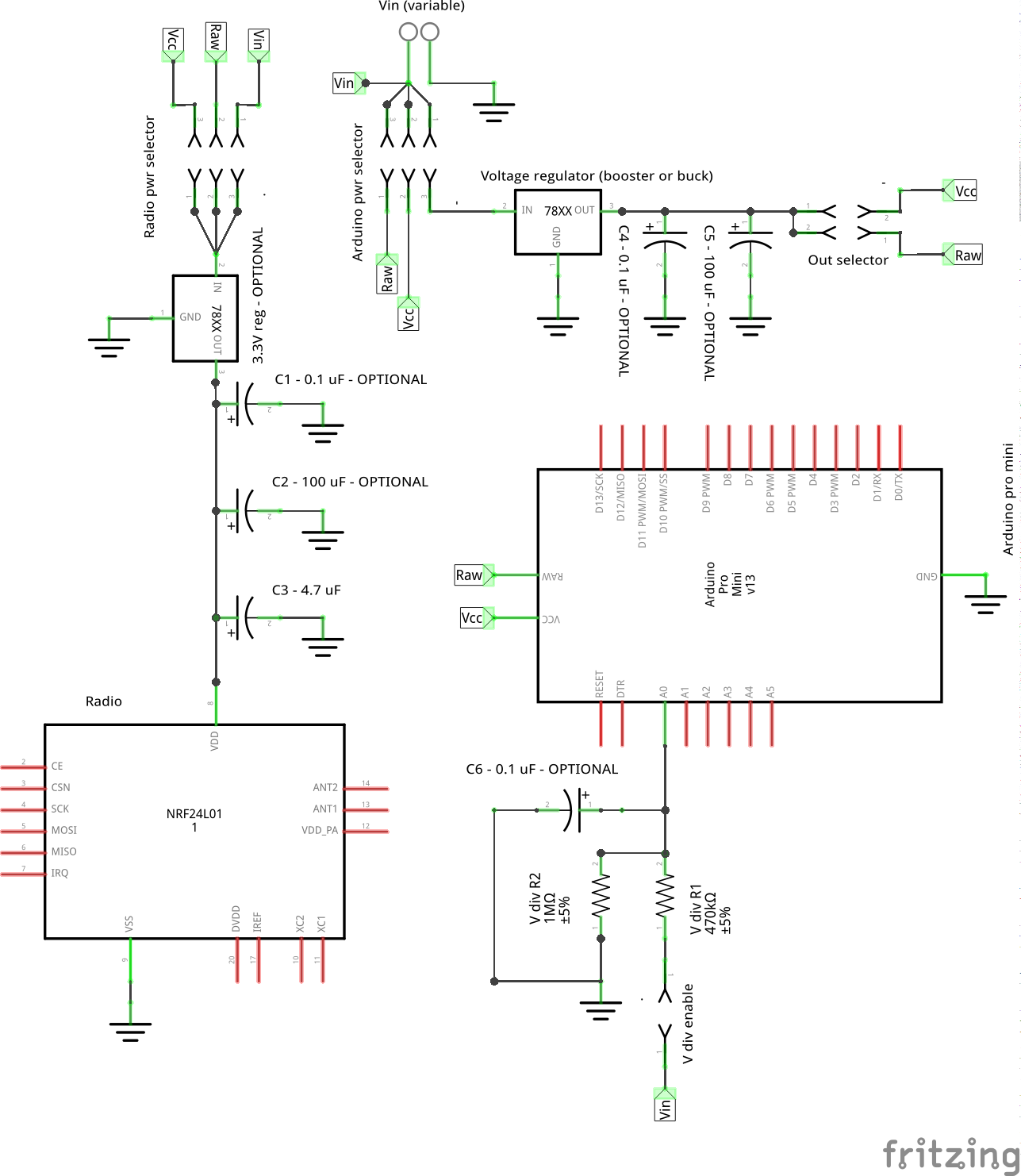
Here is the schematic of the modified power section.
I think that, with this schematics and the appropriate hardware choice, it is possible to cover a large number of power supply options (regulated and unregulated power input, 5V and 3.3V pro mini, 2xAA battery, 12Vin, 24Vin, 9V battery, TP4056 + 18650 Li-Ion cell, daughter board power source, etc...) , simply changing a couple of jumpers.
About daughter board... I don't know which is the best connection option for the Vraw pin of the MysX connector... Raw or Vin? Maybe Vin...
Let me know what you think and if it can be useful. Sorry for the long post and bad english.
-
Hi guys, this is my firs post here, so thank you for the amazing work! :+1:
I'm working on a multisensor (3 x Pir, 1 x DHT22, 1 x LDR, 1 x OLED display, 1 x WS2812B led ring for signaling and as small RGB lamp, 1 capacitive touch button) with an arduino pro mini 3.3V (8 Mhz) and NRF24L01+, all placed in a hexagonal custom case (3d printable).The sensors has also a TP4056, a 18650 Li-Ion battery and a step-up boost converter to power the arduino (raw pin) and all the other components. The radio is powered through the arduino Vcc Pin (3.3 V) and all works quite good on a breadboard.
Now I'm in the soldering phase (perfboard) but this task is very time consuming and this technique gives a "non professional" looking to the inside of the node, so I have found this easy-newbie pcb and it is great! Thank you for sharing this!
So my plan is to use this pcb instead of three different perfboard but I think that at the moment the power section is not fully compatible with my setup, but with some modification it will be OK and this modifications could allows more flexibility in the power options for the pcb.
Off course I don't have the skills to directly design and share a modified pcb, so I'm writing here my idea with the hope that, if it is useful, someone can implement it.
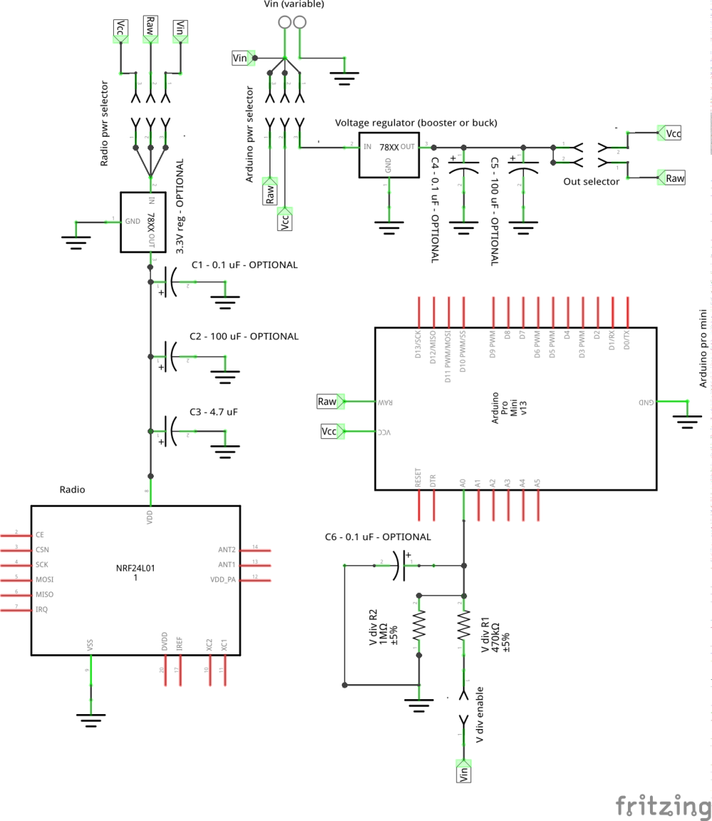
Here is the schematic of the modified power section.

I think that, with this schematics and the appropriate hardware choice, it is possible to cover a large number of power supply options (regulated and unregulated power input, 5V and 3.3V pro mini, 2xAA battery, 12Vin, 24Vin, 9V battery, TP4056 + 18650 Li-Ion cell, daughter board power source, etc...) , simply changing a couple of jumpers.
About daughter board... I don't know which is the best connection option for the Vraw pin of the MysX connector... Raw or Vin? Maybe Vin...
Let me know what you think and if it can be useful. Sorry for the long post and bad english.
-
@franz-unix I'd go for a LDO (le33 or mcp1700) to power the board and remove all voltage regulators
@gohan The part numbers in the schematics are just for example because the aim of the proposed modifications to the power section of the easy newbie pcb is to allow more flexibility in the power options.
For example:
2 x AA battery powered node + Pro mini 3.3V:
- Arduino Power Selecor -> short with a jumper the pin at the right end (1 and 3)
- Install a 3.3V fixed output boost converter
- Out selector: short wit a jumper the pins 1 and 2 and go to Vcc Pin of the pro mini
- Radio Pwr Selecor->Short with a jumper the pins 1 and 3 to power the radio directly from the battery
- Bypass with a wire the Vin and Vout of the Optional 3.3V voltage regulator
- Enable with a jumper the V div circuit to measure the battery voltage
3.3 V regulated Vin + Pro mini 3.3V:
- Arduino Power Selector -> short with a jumper the pins in the middle (2 and 2)
- Radio Pwr Selector->Short with a jumper the pins at the right end (1 and 3) to directly power the radio
- Bypass with a wire the Vin and Vout of the Optional 3.3V voltage regulator
5 V regulated Vin + Pro mini 3.3V:
- Arduino Power Selector -> short with a jumper the pins at the left corner (3 and 1) to power the pro mini through RAW pin
- Radio Pwr Selector->Short with a jumper the pins at the left end (3 and 1) to power the radio from the pro mini Vcc out (3.3V)
- Bypass with a wire the Vin and Vout of the Optional 3.3V voltage regulator
9V battery power node and pro mini 3.3V:
- Same configuration of 5 V regulated Vin + Pro mini 3.3V:
12V/24V regulated Vin + Pro mini 3.3V:
- -Arduino Power Selector -> short with a jumper the pin at the right end (1 and 3)
- Install a 3.3V fixed output Voltage regulator
- Out selector: short wit a jumper the pins 1 and 2 and go to Vcc Pin of the pro mini (or go to the raw pin if a 5V Vreg is used
- Radio Pwr Selector->Short with a jumper the pins at the left end (3 and 1) to power the radio from the pro mini Vcc out (3.3V)
- Bypass with a wire the Vin and Vout of the Optional 3.3V voltage regulator
And so on... Is possible to find the right combination of hardware and jumper also for a 5V pro mini
One other possibility is to power the pcb through a daughter board and MysX connector. This increase significantly the power options (220 AC, Li-ion batteries) like for example with the use of an AC/DC converter (HLK-PM01), a tp4056 Li-Ion battery charger and so on, directly soldered on the daughter board
-
The final goal is to have one pcb that is suitable for a large numbers of node types.
This reduce the time of building, make the soldering process easier and gives a more "professional" and robust final result.
Having one single pcb makes also my life easier when I have to design a 3d printable case and when I have to place the components inside.
-
And... after a while and some googling & Kicad learning, I have designed my first pcb.
Below the final result
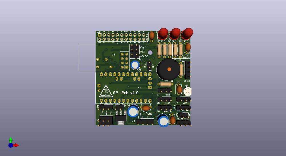
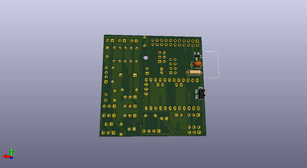
At the moment it is not tested but after that if someone is interested I can share it in openhardware.
Below the schematic
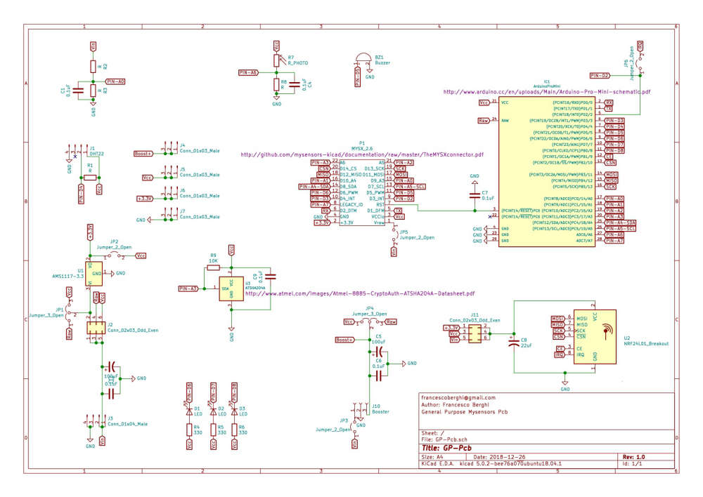
Any suggestion / improvement / comment is well appreciated.

