In wall light switch node - Custom PCB
-
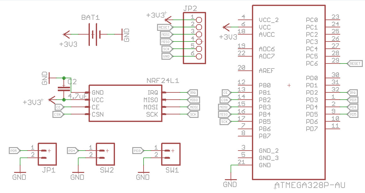
I have attached the Board and Schematic mock-ups. Would it be possible to hear your opinions on what needs to be changed, if anything that is. All being well the RF Module fits where i intend it too, sitting just above the chip itself.
Does that capacitor look okay being grounded to the ground line rather than directly onto the ground pin of the RF module (To stabilize the vcc and ground of the RF module).
A quick little list to show what is what on the board:
AVR CONNECT - Connection for AVR Programmer to bootload.
SW1 - Screw terminals for Switch 1.
SW2 - Screw terminals for Switch 2.
SW3 - Screw terminals for Switch 3.
ATMEGA328P-AU - The obvious, ATMEGA328P-AU.
NRF24L1 - NRF24l01+, will use header pins and solder so its sitting just abover the ATMEGA.
C2 - 4.7uF Capacitor to bridge the VCC and GND on the radio.
BAT1 - Cell coin holder (CR2450)I don't need any mounting holes at the moment so that isn't an issue. I plan on elevating it off of the metal back box to stop any chance of shorting too.
Would you say that i need to be wiring the terminals for the switch using VCC and a resistor or would a input pin to ground be okay? I've seen so many people people do it both ways in the forums and on the general internet, what is the preferred method?
I'm more than happy with receiving any sort of criticism on this board, as this is my first attempt of a custom PCB and my first attempt of using Eagle software.
-
Why not use a 4-pol screw terminal instead? One common and then one input for each switch. Also, consider if the corners could be 45 degrees instead of 90. That would make it fit more easly in a round back box. Aren't you missing a pull-up for reset and a few decoupling caps for the ATMega?
-
Indeed, decoupling cap (100nF) is needed or the powerline (VCC-GND) would be unstable when transmissions occur. This effect could block or reset the atmega.
With this setup, you will not be able to program sketches when the NRF is connected. If you add an FTDI header, you can program via serial port and monitor the processor while the NRF is connected. Will help in debugging code. -
Why not use a 4-pol screw terminal instead? One common and then one input for each switch. Also, consider if the corners could be 45 degrees instead of 90. That would make it fit more easly in a round back box. Aren't you missing a pull-up for reset and a few decoupling caps for the ATMega?
@mardah @GertSanders - Sorry guys, for some reason i just assumed that the decoupling caps were only needed for if i was using an external crystal, for increased power needed for 16MHz. I'll get that on.
I'm going to have a look at that header you speak about when i get home tonight, i was planning on programming the board then soldering the RF module on. Now you point this out that would be a very silly amature mistake to do. Thank you for making that obvious.
I'm also planning on refining the layout of the board and the shape. So i will take the corners off to adapt it to a round box.
-
You might want to have both the 1x6 pin FTDI-serial-"arduino" port and the 2x3 pin AVR ISP port. Note that pin# are standardized.
-
You might want to have both the 1x6 pin FTDI-serial-"arduino" port and the 2x3 pin AVR ISP port. Note that pin# are standardized.
@m26872 Could i ask why i would need both? They essentially do the same thing, right? Except FTDI uses the DFU bootloader and then the SPI connection overrides the DFU bootloader, am i correct in thinking this or do i have my lines mixed up? If so then i was planning on using the 6 pins i have on the edge of the board, connect them via jumper cables to the 6pin SPI connecter that would come with the USBasp programmer i plan to purchase. The reason i plan to go down this route is simply to save room in the socket, limited height room.
@GertSanders - Is the 6 pins that i have added to the board not a FTDI header? What makes it not, the pin layout or the pins used on the mega chip? I thought that if i added 6 pins, wired them to the chip using the pins i have (gnd, vcc, ce, csn, irq, miso, mosi and sck) that made it a FTDI, I'm guessing I'm incorrect?
@mardah - Free space depending, i'm looking into doing this now, so do you feel that my switching method is sufficient enough without using vcc and a resistor to each switch and then to the input pin? You're happy with the Input pin -> switch -> GND method? EDIT: The only 4 Pol i can find that would be big enough to accept 3 cables into the common is working out at a stupid price in comparison to the rest of the board. At the moment, i will be using the 3 terminal setup i have currently sketched.
I planned on using this as the USBasp programmer, however if i can use just an FTDI connection to do both (program the MYSBootloader and to upload sketches) that would be better for saving space on the board.
The FTDI programmer: Link
Can you use this to program the MYSBootloader as well as upload a sketch or is this simply to upload a sketch to the mega?The decoupling caps, as a rule of thumb, its 100nF cap per supply pin, correct? I will supply all 3 VCC pins with the power, so i should connect a 100nF cap to each of the pins. Does this sound over kill or okay?
-
Why not use a 4-pol screw terminal instead? One common and then one input for each switch. Also, consider if the corners could be 45 degrees instead of 90. That would make it fit more easly in a round back box. Aren't you missing a pull-up for reset and a few decoupling caps for the ATMega?
@mardah If i wire a 4-Pol screw terminal as follows:
1 - GND
2 - INPUT1
3 - INPUT2
4 - INPUT3Then i wire GND into Switch1's COM connector, then L1 goes to screw terminal pin 2 (INPUT1). Then i take the com from the back of Switch1 into the COM connector of Switch2, then wire Switch2's L1 connector to screw terminal pin 3 (INPUT2) and the same for switch 3. Do you feel this would work as intended?
-
hi.
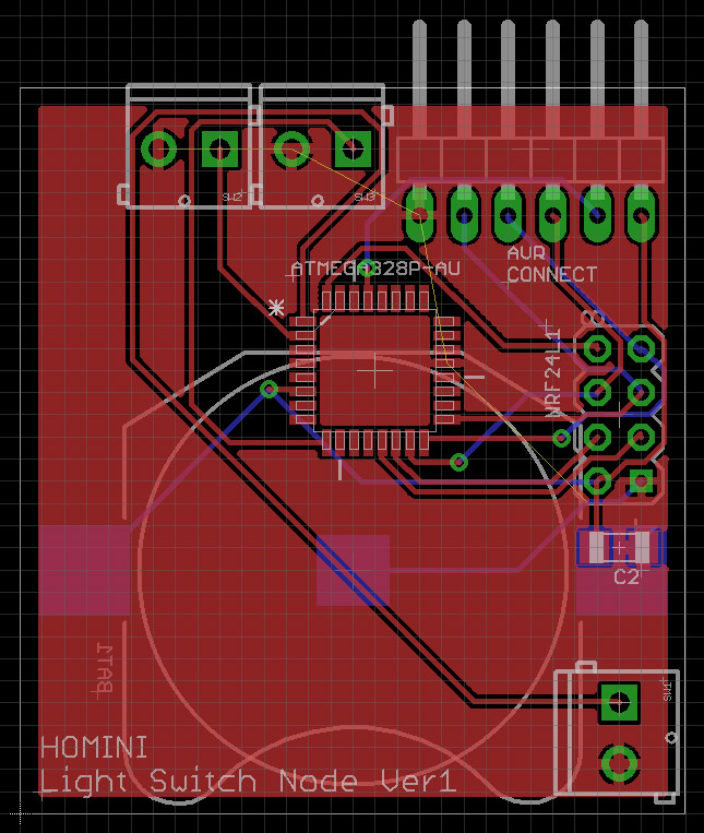
just a little thing, it is "better" to have nothing under radio antenna (no gnd plane..) for range and operation. it could help as it will be inwall ;)
-
hi.
just a little thing, it is "better" to have nothing under radio antenna (no gnd plane..) for range and operation. it could help as it will be inwall ;)
-
@m26872 Could i ask why i would need both? They essentially do the same thing, right? Except FTDI uses the DFU bootloader and then the SPI connection overrides the DFU bootloader, am i correct in thinking this or do i have my lines mixed up? If so then i was planning on using the 6 pins i have on the edge of the board, connect them via jumper cables to the 6pin SPI connecter that would come with the USBasp programmer i plan to purchase. The reason i plan to go down this route is simply to save room in the socket, limited height room.
@GertSanders - Is the 6 pins that i have added to the board not a FTDI header? What makes it not, the pin layout or the pins used on the mega chip? I thought that if i added 6 pins, wired them to the chip using the pins i have (gnd, vcc, ce, csn, irq, miso, mosi and sck) that made it a FTDI, I'm guessing I'm incorrect?
@mardah - Free space depending, i'm looking into doing this now, so do you feel that my switching method is sufficient enough without using vcc and a resistor to each switch and then to the input pin? You're happy with the Input pin -> switch -> GND method? EDIT: The only 4 Pol i can find that would be big enough to accept 3 cables into the common is working out at a stupid price in comparison to the rest of the board. At the moment, i will be using the 3 terminal setup i have currently sketched.
I planned on using this as the USBasp programmer, however if i can use just an FTDI connection to do both (program the MYSBootloader and to upload sketches) that would be better for saving space on the board.
The FTDI programmer: Link
Can you use this to program the MYSBootloader as well as upload a sketch or is this simply to upload a sketch to the mega?The decoupling caps, as a rule of thumb, its 100nF cap per supply pin, correct? I will supply all 3 VCC pins with the power, so i should connect a 100nF cap to each of the pins. Does this sound over kill or okay?
@samuel235 I can't tell you what you need, I'm just saying that if you provide an AVR-ISP port looking like FTDI-port, everyone except yourself will be confused or even risk to destroy the AVR by mistake.
Let's look at the Sensbender diagram as a reference. The FTDI-port is JP2 and the AVR-ISP is JP3. Most people would prefer to program bootloader once and then use the FTDI to upload and debug new programs.
If I couldn't fit an AVR ISP port, I would try to make to make the nRF SPI-pin + Reset, accessible. Maybe even better is to make (if you don't already have?) a special board for 328p-AU (TQFP-package) bootloader programming, then solder it in place with bootloader already on it.
Please also note that the JP2 FTDI-port needs R3 and C5 to work. -
@samuel235 I can't tell you what you need, I'm just saying that if you provide an AVR-ISP port looking like FTDI-port, everyone except yourself will be confused or even risk to destroy the AVR by mistake.
Let's look at the Sensbender diagram as a reference. The FTDI-port is JP2 and the AVR-ISP is JP3. Most people would prefer to program bootloader once and then use the FTDI to upload and debug new programs.
If I couldn't fit an AVR ISP port, I would try to make to make the nRF SPI-pin + Reset, accessible. Maybe even better is to make (if you don't already have?) a special board for 328p-AU (TQFP-package) bootloader programming, then solder it in place with bootloader already on it.
Please also note that the JP2 FTDI-port needs R3 and C5 to work.@m26872 Firstly, thank you for referencing the sensebender and its pinout. I can now have a look at this and use it to better improve the pinout and layout of my board. So, i will try to get both headers onto my board to allow better programming capabilities. If i use the same pinout as the sensebender does for the AVR ISP and the FTDI-port, would i then be able to burn the bootloader and upload sketches while the RF module is soldered. If not, do you think i could use some jumper headers to effectively remove the RF module from the board while I upload the sketch and then put the jumpers back on to close the circuit back up?
MySensors 2.1.1
Controller - OpenHAB (Virtual Machine)
Gateway - Arduino Mega MQTT Gateway W5100 -
@m26872 Firstly, thank you for referencing the sensebender and its pinout. I can now have a look at this and use it to better improve the pinout and layout of my board. So, i will try to get both headers onto my board to allow better programming capabilities. If i use the same pinout as the sensebender does for the AVR ISP and the FTDI-port, would i then be able to burn the bootloader and upload sketches while the RF module is soldered. If not, do you think i could use some jumper headers to effectively remove the RF module from the board while I upload the sketch and then put the jumpers back on to close the circuit back up?
@samuel235 I can't recall that I've actually used the ISP with the nRF, but the whole point of ISP is that it should work.
-
@samuel235 I can't recall that I've actually used the ISP with the nRF, but the whole point of ISP is that it should work.
@m26872 Okay, so its probably best to just burn the bootloader, then solder the nRF inplace and then upload the sketches using the FTDI port just in case i solder on the nRF then turns out i can't burn the bootloader?
I believe i can leave the AREF pin unconnected. Is this true?
Do you have any other input other than the following changes i'm scheduling to make on the board tomorrow:
- Remove GND plane around the area of nRF module to reduce chance of interference.
- Remove current screw terminals and replace with 1 4-Position with GND as common and other 3 going to input pins.
- Connect all GND pins.
- Connect all VCC pins.
- Add decoupling Caps in the layout that Sensebender uses, 1 on each VCC, so 3 in total.
- Add Pullup to reset pin.
- Remove current 'FTDI' connector and add correct FTDI layout connector along with a SPI header connection for bootloading, use Sensebender for reference of the pinout for these two connectors.
While looking through the Sensebender schematic and images, i have noticed there is Q1 (What i think is a transistor, correct me if i'm incorrect), may i ask if you know what this is for, as it is not actually on the final board images.
Sorry if i have made any more school boy errors.
Sam.MySensors 2.1.1
Controller - OpenHAB (Virtual Machine)
Gateway - Arduino Mega MQTT Gateway W5100 -
@m26872 Okay, so its probably best to just burn the bootloader, then solder the nRF inplace and then upload the sketches using the FTDI port just in case i solder on the nRF then turns out i can't burn the bootloader?
I believe i can leave the AREF pin unconnected. Is this true?
Do you have any other input other than the following changes i'm scheduling to make on the board tomorrow:
- Remove GND plane around the area of nRF module to reduce chance of interference.
- Remove current screw terminals and replace with 1 4-Position with GND as common and other 3 going to input pins.
- Connect all GND pins.
- Connect all VCC pins.
- Add decoupling Caps in the layout that Sensebender uses, 1 on each VCC, so 3 in total.
- Add Pullup to reset pin.
- Remove current 'FTDI' connector and add correct FTDI layout connector along with a SPI header connection for bootloading, use Sensebender for reference of the pinout for these two connectors.
While looking through the Sensebender schematic and images, i have noticed there is Q1 (What i think is a transistor, correct me if i'm incorrect), may i ask if you know what this is for, as it is not actually on the final board images.
Sorry if i have made any more school boy errors.
Sam.@samuel235
Arduino Pro Mini should be your no1 reference. Schematics and Eagle files povided. There your can see the normal layout of Q1 e.g. It's the crystal/oscillator (with 22pF caps if you choose xtal) I don't know why Sensebender looks like it does.I haven't studied your design closely or know your intentions, but I don't know of any proven coin cell nRF designs, but I suppose you'll have it sleeping a lot.
Sometimes it's good to breadboard prototypes if there're any hesistance.
-
for coincell, maybe you could add a capacitor near the coincell to absorb spike of power consumption..so the coincell would not discharge too fast with sudden spike ;)
maybe 47u or 100u if you add few sensors in future...100u not very cheap..maybe through hole, there are some not too big. -
@samuel235
Arduino Pro Mini should be your no1 reference. Schematics and Eagle files povided. There your can see the normal layout of Q1 e.g. It's the crystal/oscillator (with 22pF caps if you choose xtal) I don't know why Sensebender looks like it does.I haven't studied your design closely or know your intentions, but I don't know of any proven coin cell nRF designs, but I suppose you'll have it sleeping a lot.
Sometimes it's good to breadboard prototypes if there're any hesistance.
@m26872 I have been looking at a nano i have on my desk while building these designs, and i didn't notice anything with Q1 hense why i asked about it on sensebender. However it is not of any interest to this project (to my knowledge), i just wanted to learn the use of a tran in this case.
I will be sleeping the module quite a bit yeah, literally asleep all the time until someone presses the switch.
@scalz I'll throw a 47u in there, this node shouldn't be used for any other sensor at any time to be honest, hence why i'm designing it from scratch to go into the socket.
-
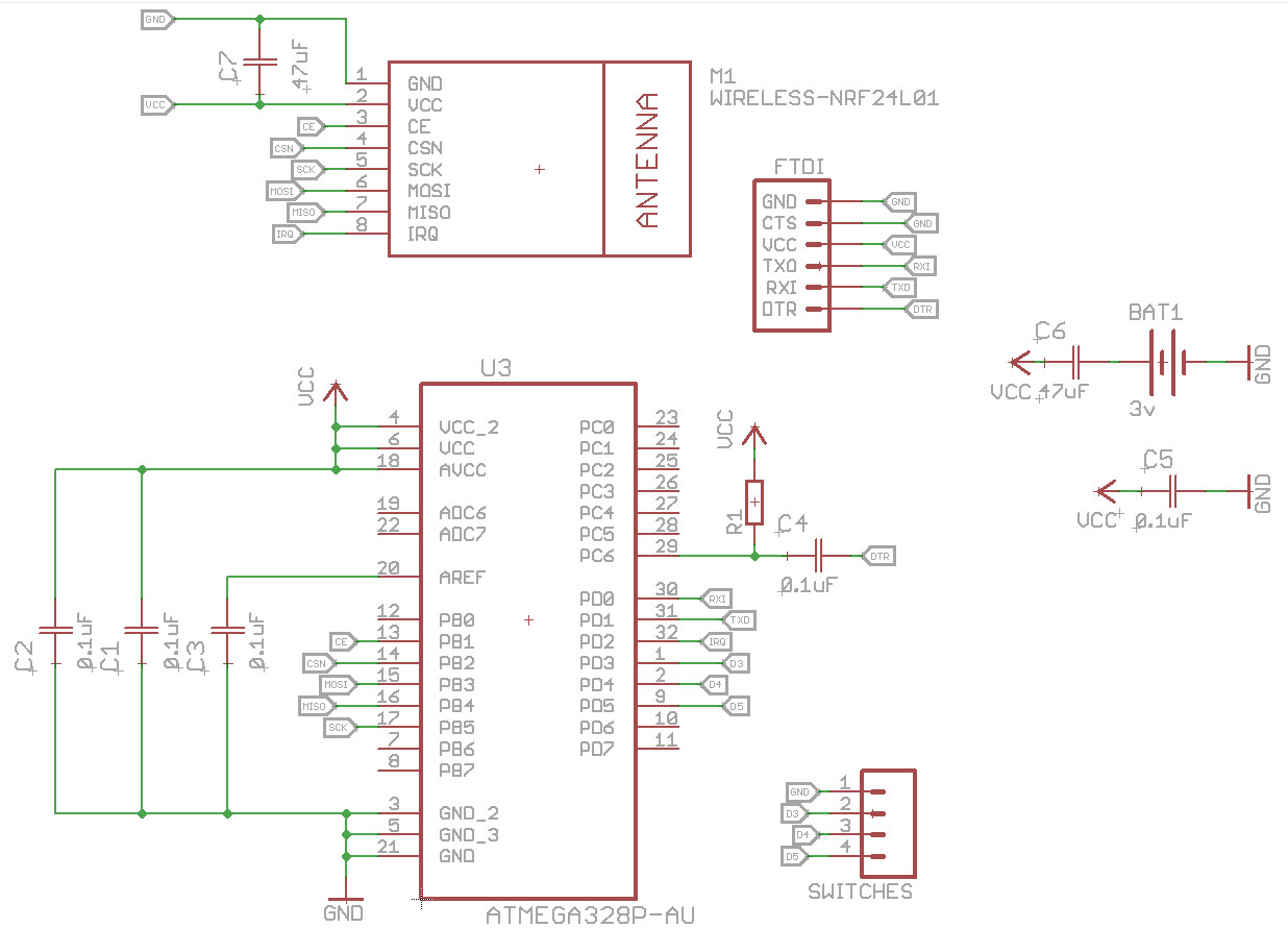
Tonight i have finished updating my schematic to reflect some of your helpful inputs. Please, again, throw any comments you have regarding my layouts my way so i can further improve the board if needed. Upgrades i have done are:
- Added Capacitors for the VCC lines.
- Added proper pinout/layout for the FTDI header.
- Added a Capacitor on the battery to stop any spikes of current draw.
- Changed the double position screw terminals for a 4 position one.
- Added a pull-up resistor and capacitor on reset pin for the FTDI uploads to be able to reset upon new sketch upload.
Currently i still do not have a SPI header included. Would i be able to survive without one, could i do the sketch upload through the FTDI header at all?
Once i finalize the overall board layout i will know what size i'm working with and IF i can fit a SPI header in, i will install one onto the board. However, because of the limiting space i may struggle on this.
-
Looks proper. I think those two 47uF caps don't necessarily have to be two and can be placed anywhere between vcc and gnd, provided short low resistance traces etc.
-
Looks proper. I think those two 47uF caps don't necessarily have to be two and can be placed anywhere between vcc and gnd, provided short low resistance traces etc.
-
Either you breadboard your design first or make it a flexible pcb design.
Add footprint and make room for bigger or more caps just in case they'll be needed. The physical place shouldn't matter.
Edit: Since someone will object to that last sentence if I don't clarify it .... Physical place of that 47uF near nRF could matter, but if so - it should be fixed with some small low ESR cap near it instead.