Yet Another RGB driver (activeRGB)
-
@scalz Thanks for your comment. ..means I need to read some more. I am not sure I completely understand the concept yet!
I tried uploading my kicad_brd file at OSHpark and it looks good, though I am not sure about solder mask.
I think I should not rush and read up on ground plane and soldermask before I submit the file for fab.
The nice part about OSH (even though its pricier than dirtyPCB) is that it takes pcb file directly so I dont have to deal with the various formats....or am I mistaken and the info is embedded in the file?
Let me go read more about GND planes and see what I need to do.
-AM
@activemind I can only agree with Scalz here, i would impliment it. And next board you do, implement it at the start, means less routes are required.
-
@Samuel235 Thanks for the advice. I will try to do it.
Also, what fab house would yuou recommend for 2-3 prototypes and then maybe I can shift it to dirtyPCB. OSHpark?
-AM
-
Reading some more and playing around with the tool I "think" I understand what its trying to do.
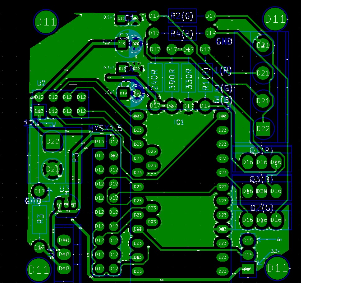
So I created a "pour" on the front for GND plane and the PCB now looks like this:
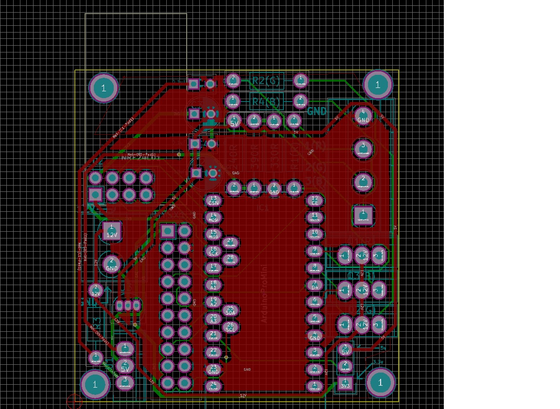
What do I want to do on the back? Create another GND pour?
-AM
-
Try out PCBWay, they're doing the first order for free. However you have to generate gerber files for them, in fact, to my knowledge OSHPark are one of very few to allow .brd files. I'm going to be doing a review for PCBWay soon on here, all i'm saying for now is they are fantastic service providers.
Yes create a GND plane for the back too. I always have GND on front and back. I know some that have a VCC plane on one, but that depends on the components you use. Stick to GND on both to keep it simple.
-
yes.
as you can see, it greatly simplify your old gnd routing. guess if you had started by doing this ;)
and then, in future design, it would be possible to use vias if you need to fill some area where you can't have gnd because of other routing. same plane things for power etc... be careful, never put a gnd pour for AC lines, avoid when you can under antenna etc... there are some basics & advanced rules. but you will learn :) -
@Samuel235 Thank you once again for all your help and feedback.
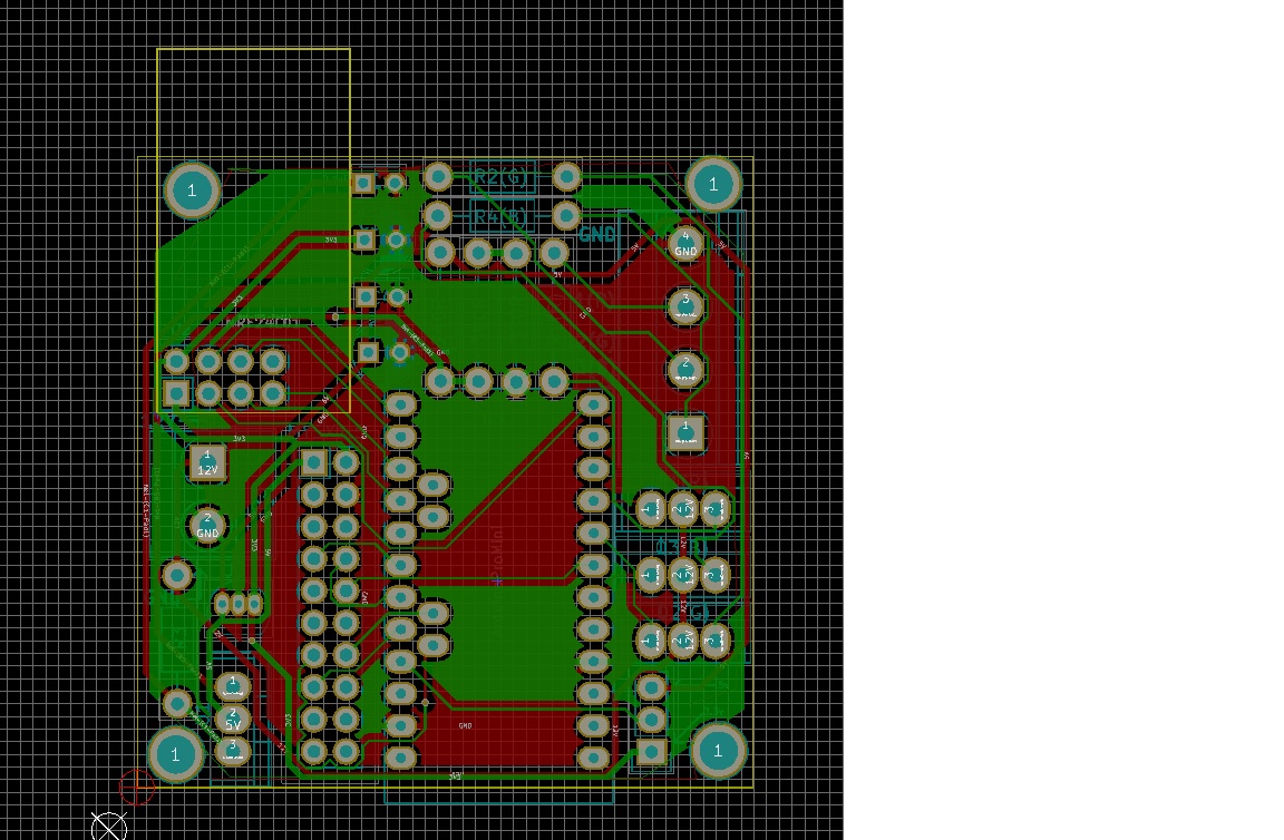
Here is what it looks like after a GND pour on the back.
I really want to add a OSH and Mysensors silkscreen on the front or back but I will have to learn how to do that. Am I getting too ambitious here :-)
-AM
-
yes.
as you can see, it greatly simplify your old gnd routing. guess if you had started by doing this ;)
and then, in future design, it would be possible to use vias if you need to fill some area where you can't have gnd because of other routing. same plane things for power etc... be careful, never put a gnd pour for AC lines, avoid when you can under antenna etc... there are some basics & advanced rules. but you will learn :)@scalz said:
yes.
as you can see, it greatly simplify your old gnd routing. guess if you had started by doing this ;)
and then, in future design, it would be possible to use vias if you need to fill some area where you can't have gnd because of other routing. same plane things for power etc... be careful, never put a gnd pour for AC lines, avoid when you can under antenna etc... there are some basics & advanced rules. but you will learn :)I will have to read the above comment multiple times for it to sink through :-)
I tried to place NRF sticking out of the board so that there is no GND plane below the antenna. Do you see an issue in the PCB pic above with respect to antenna?
-AM
-
Here is what the gerber view looks like -
Front Gerber:
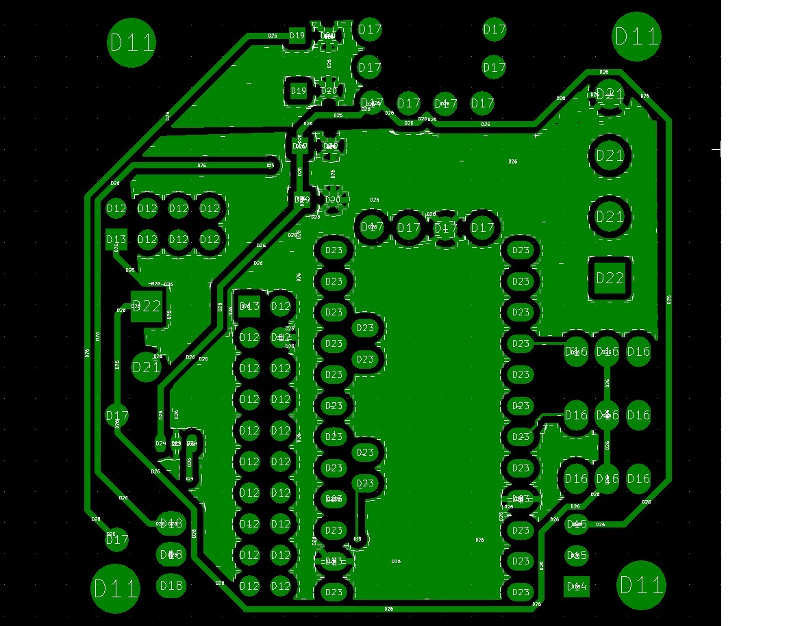
Back Gerber:
Front Silkscreen:
Comments?
-AM
-
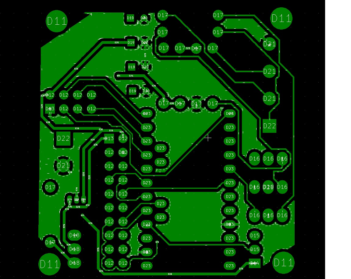
Here is what the gerber view looks like -
Front Gerber:
Back Gerber:
Front Silkscreen:
Comments?
-AM
@activemind, never too ambitious. Don't ever let anything stop you achieving what you want.
The gerber files, i'm sure the front silkscreen shouldn't have any signs of the copper traces on. It should only be what you intend to see written/drawn on the surface of your board.
-
@Samuel235 Hmmmm, let me go back and see what went wrong with my silkscreen. My impression too was that it would show only the txt but when I file showed something different I put it up for review :-) Glad I did.
Also, looking into OSH silkscreen!
-AM
-
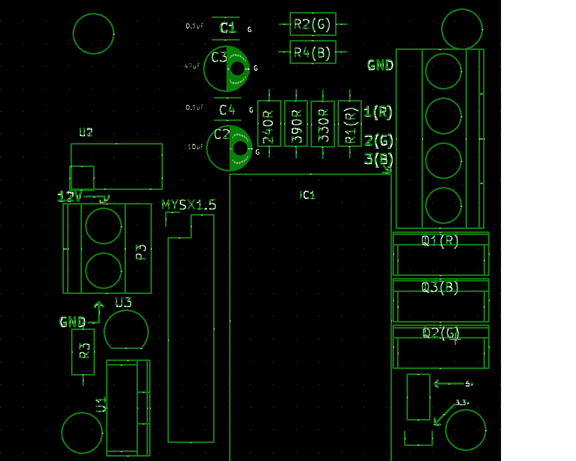
Looked at the silkscreen file and I had pulled up the wrong file in gerber view. Here is what the correct silkscreen looks like:
-AM
-
Done! Sent the files to Itead for processing :-)
Lets see if the boards work when they come back!
Thanks for all your help @Samuel235 and @scalz
-AM
-
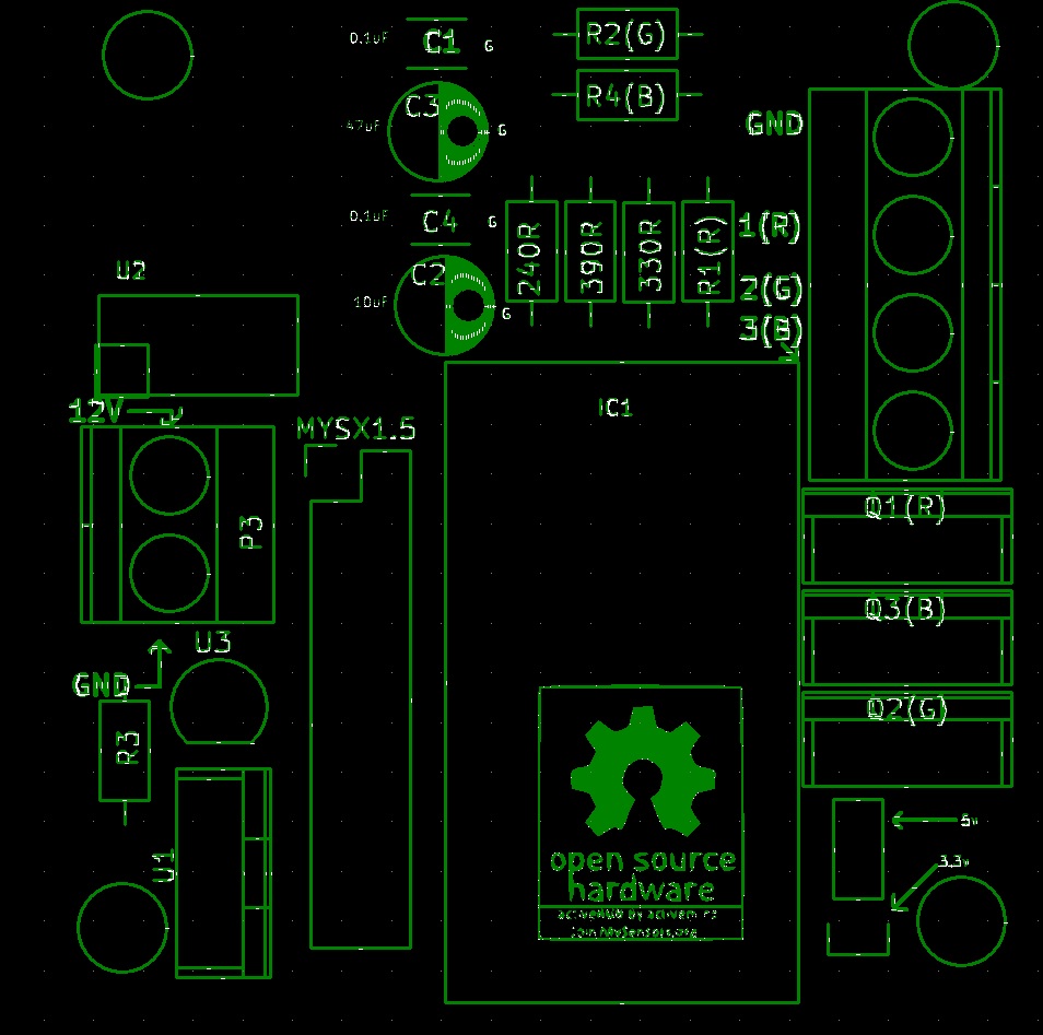
managed to add the OSH and mysensors silkscreen I was thinking. Here is the final silkscreen...
-
Received an update from Itead. Everything looks good in gerber files. They have sent it to fab.
Now the wait starts...
-AM
-
Another update from Itead...PCBs complete and shipped!
Cant wait to get my hands on my first PCB :-)
-AM
-
PCBs are in.... :-)
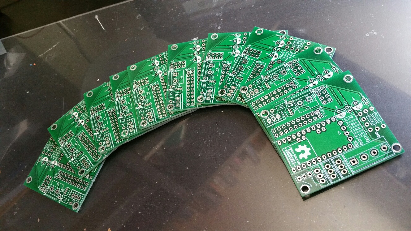
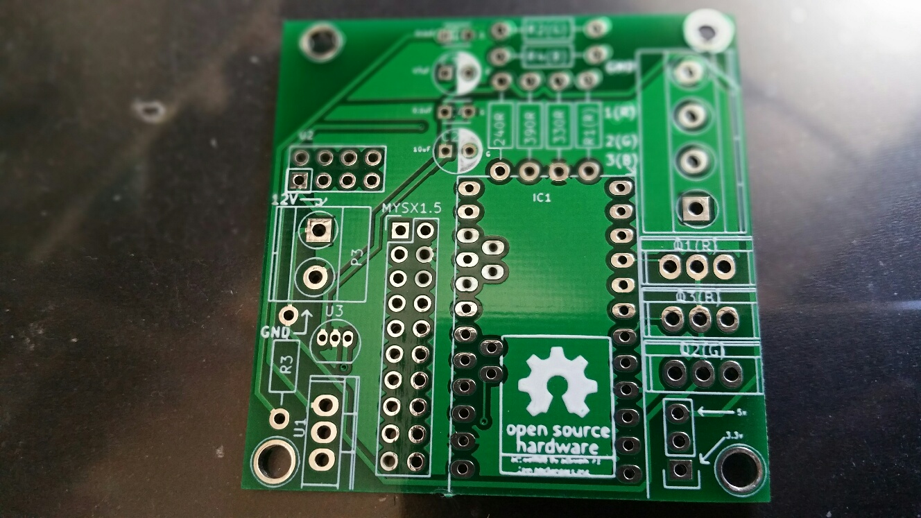
Time to populate them now and see if they work :-)
-AM
-
Damn! Just realized some of my parts are still not in....
Anyways, looking at the PCB,
- I think some of the text is just too small, like the cap values and OSH silkscreen. I need to make them bigger if I do a next rev.
- The mounting holes are a little too big. This is lightweight PCB and should not need heavyduty M3 screw. I could probably go with smaller mounting holes.
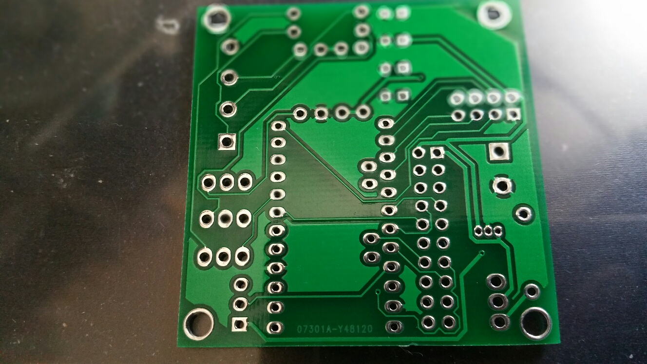
- Some silkscreen on the back would be nice...else it just looks naked :-)
-AM
-
@jeti Thank you. Unfortunately havent had a chance to assemble the boards yet. Have all the parts in but life gets in the way :-)
-AM
-
@jeti Thank you. Unfortunately havent had a chance to assemble the boards yet. Have all the parts in but life gets in the way :-)
-AM
@activemind
do you already have a BOM? and is there chance to help you out? I would be willing to assemble one or two of the boards :bowtie: