CNC PCB milling
-
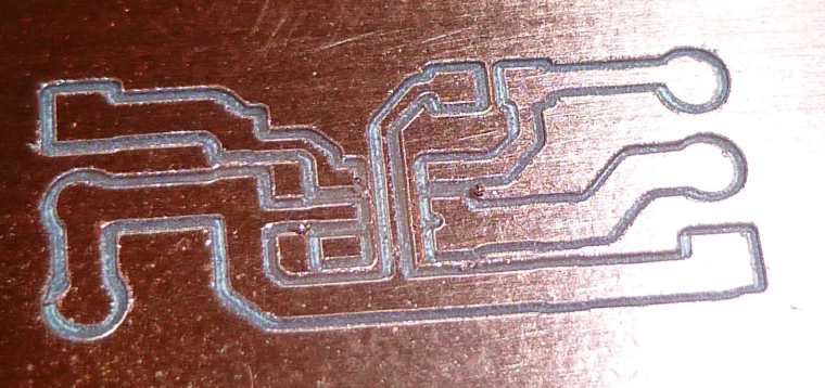
Exact same procedure as last time, except this time using the Model 20 and a different etching pattern:
Meh, I'm not sure it's really an improvement. The model 20 jbit ust doesn't seem to cut as cleanly as a Jack bit.
BTW, I increased the windows task priority of the browser (and, there, Chilipeppr) and also the serial port jason server, both to High. Since then I haven't had any probe failures. Causation, or luck? Time will tell.
-
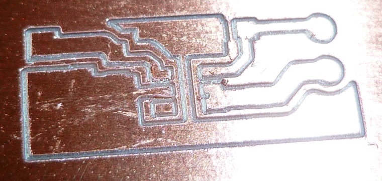
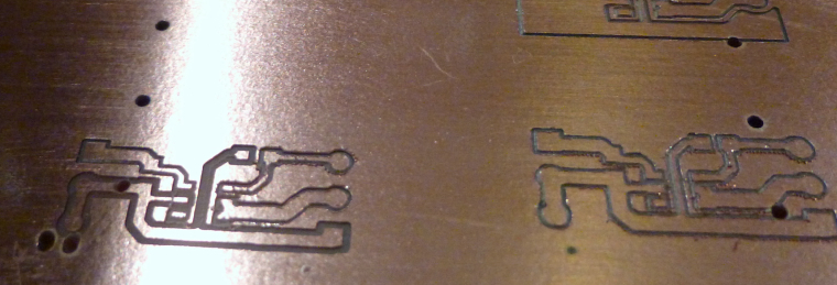
So, I decided to relax the constraints and go for something easier, like a simple circuit for a load switch that uses an SOT23-6 and three 0603 SMD components:
The etching came out perfect the very first time. :) I cut it using a new Jack bit, and I cut it to a depth of z=-0.15 using three flatcam passes, each -0.05 deeper than the prior one. I tested it with a contuinity meter, and isolation is perfect. :)BTW, I used OpenCNCPilot to break line segments down to 0.5mm, and I probed the board surface at 1mm for the autoleveling.
Next, I need to try soldering it to see what life without solder mask is like. To that end, would I be better off with wider cuts?
@neverdie said in CNC PCB milling:
So, I decided to relax the constraints and go for something easier, like a simple circuit for a load switch that uses an SOT23-6 and three 0603 SMD components:
The etching came out perfect the very first time. :) I cut it using a new Jack bit, and I cut it to a depth of z=-0.15 using three flatcam passes, each -0.05 deeper than the prior one. I tested it with a contuinity meter, and isolation is perfect. :)BTW, I used OpenCNCPilot to break line segments down to 0.5mm, and I probed the board surface at 1mm for the autoleveling.
Next, I need to try soldering it to see what life without solder mask is like. To that end, would I be better off with wider cuts?
I think ideally the CNC would remove all of the extraneous copper that's near the pads. That way there'd be no risk of solder bridging to the extraneous copper. However, how to do that? The software doesn't obviously support removing extraneous copper.
Here's an example:
 )
) -
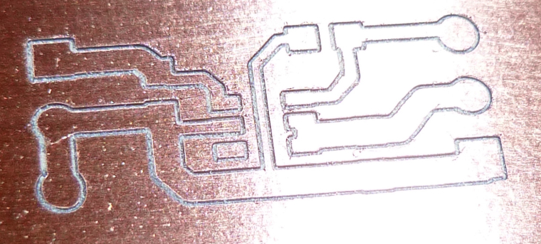
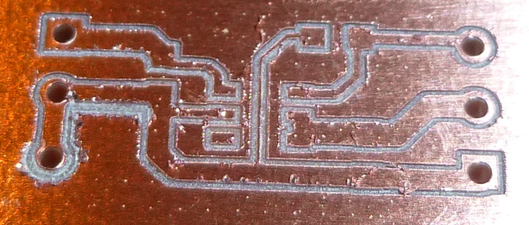
Here's the Model 20 bit again, but this time with flatcam being told that its width is 0.25mm:
The pad widths are just not as uniform as with the Jack bit. On the other hand, it looks like it should be less prone to solder bridging.
-
@andrew How are you managing the alignment on your double sided boards, such that when you flip the PCB over to mill the other side too, all the via holes, etc., are lined up where they should be?
@neverdie said in CNC PCB milling:
Here's the Model 20 bit again, but this time with flatcam being told that its width is 0.25mm
how flatcam told you the width or how do you calculate the tool width? it should be specified by you, flatcam does not know how to calculate the tool width in case of carving bits, it varies with the milling depth and depends on the tip's angle and end width. please see the corresponding mathematic formula mentioned in my previous posts.
you have to generate the isolation routing G code for a specific tool/bit, it cannot be re-used for a different sized one.
- flatcam supports double sided pcb milling with proper alignment holes. using them the isolation routing will be precisely aligned on both sides. you have to drill the alignment holes first, then make the isolation routing on the bottom side, then turn the pcb and finish the isolation routing and the drilling on the top side. it is also highlighted on flatcam's website: http://flatcam.org/manual/procedures.html#side-pcb
- for isolation routing it is useless to make multiple passes for multiple depth.
- to make the isolation routing width larger, you should use multiple passes. this is necessary to create a large enough isolation width. to be sure that all copper will be removed between the different passes (e.g. due to cnc inaccuracy or backlash) you should use overlapping. see http://flatcam.org/manual/procedures.html#wide-isolation-routing
- flatcam supports full copper removal, so it is possible to keep only the traces and pads, although with a carving bit it is very time consuming. you should use endmils for this job. see http://flatcam.org/manual/procedures.html#copper-area-clear
- it is possible to solder smd parts without solder mask, it is just question of the technique / tool. I've no problem with 0805 sized smd parts and tqfp100 housed ICs, however it is easier to do it if you have solder mask, of course. if you would like to prevent the oxidation only, then you can use tinning. for this purpose I use chemical tinning.
-
@neverdie said in CNC PCB milling:
Here's the Model 20 bit again, but this time with flatcam being told that its width is 0.25mm
how flatcam told you the width or how do you calculate the tool width? it should be specified by you, flatcam does not know how to calculate the tool width in case of carving bits, it varies with the milling depth and depends on the tip's angle and end width. please see the corresponding mathematic formula mentioned in my previous posts.
you have to generate the isolation routing G code for a specific tool/bit, it cannot be re-used for a different sized one.
- flatcam supports double sided pcb milling with proper alignment holes. using them the isolation routing will be precisely aligned on both sides. you have to drill the alignment holes first, then make the isolation routing on the bottom side, then turn the pcb and finish the isolation routing and the drilling on the top side. it is also highlighted on flatcam's website: http://flatcam.org/manual/procedures.html#side-pcb
- for isolation routing it is useless to make multiple passes for multiple depth.
- to make the isolation routing width larger, you should use multiple passes. this is necessary to create a large enough isolation width. to be sure that all copper will be removed between the different passes (e.g. due to cnc inaccuracy or backlash) you should use overlapping. see http://flatcam.org/manual/procedures.html#wide-isolation-routing
- flatcam supports full copper removal, so it is possible to keep only the traces and pads, although with a carving bit it is very time consuming. you should use endmils for this job. see http://flatcam.org/manual/procedures.html#copper-area-clear
- it is possible to solder smd parts without solder mask, it is just question of the technique / tool. I've no problem with 0805 sized smd parts and tqfp100 housed ICs, however it is easier to do it if you have solder mask, of course. if you would like to prevent the oxidation only, then you can use tinning. for this purpose I use chemical tinning.
@andrew said in CNC PCB milling:
to make the isolation routing width larger, you should use multiple passes. this is necessary to create a large enough isolation width. to be sure that all copper will be removed between the different passes (e.g. due to cnc inaccuracy or backlash) you should use overlapping. see http://flatcam.org/manual/procedures.html#wide-isolation-routing
Just to clarify that what andrew is talking about is multiple radial passes with an offset further away from the track/pads each time.
Not multiple passes in the depth.:confused: -
@andrew said in CNC PCB milling:
to make the isolation routing width larger, you should use multiple passes. this is necessary to create a large enough isolation width. to be sure that all copper will be removed between the different passes (e.g. due to cnc inaccuracy or backlash) you should use overlapping. see http://flatcam.org/manual/procedures.html#wide-isolation-routing
Just to clarify that what andrew is talking about is multiple radial passes with an offset further away from the track/pads each time.
Not multiple passes in the depth.:confused:@rmtucker said in CNC PCB milling:
@andrew said in CNC PCB milling:
to make the isolation routing width larger, you should use multiple passes. this is necessary to create a large enough isolation width. to be sure that all copper will be removed between the different passes (e.g. due to cnc inaccuracy or backlash) you should use overlapping. see http://flatcam.org/manual/procedures.html#wide-isolation-routing
Just to clarify that what andrew is talking about is multiple radial passes with an offset further away from the track/pads each time.
Not multiple passes in the depth.:confused:exactly
-
Bah! It did drill 6 holes, but it grouped them so close together that it looks like two holes instead:
I suspect an inches instead of mm error may be the culprit, but I haven't checked it yet. For sure the scaling for positioning the drill holes seems way off.
-
Strangely, flatcam seems to show roughly the correct hole size (0.9mm), yet the x and y dimensions are way off:
So, I took a wild guess that maybe it was off by a scaling factor of 25.4. Well, that did produce 6 separate holes, but they missed the target pads by a huge amount:
I'm stumped. I'm not sure where the disconnect is. Anyone seen this problem before?
-
-
@executivul I've now done a couple thousand auto-leveling probes in Chilipeppr with no probe failures. If it helps you at all, I think elevating the task priority to "High" on the browser (I use chrome) and the serial port jason is what made the difference. I've not had any probe failures at all since doing that.
-
The corrected drilling works:
The etching, though, seems to have a lot of variability in crispness from one etching to the next. -
So, I tried a couple more wild guesses, and the last guess was a match. It turns out that the scaling is off by a factor of 10x:
I have no idea why the scaling is in error, but at least now I have an antidote. :)
@neverdie why do you use any scaling factor at all? be sure you export the grbl files with proper metrics, then apply the given metrics settings in flatcam (it has global and project specific settings as well), then no scaling is necessary.
-
@neverdie why do you use any scaling factor at all? be sure you export the grbl files with proper metrics, then apply the given metrics settings in flatcam (it has global and project specific settings as well), then no scaling is necessary.
@andrew said in CNC PCB milling:
@neverdie why do you use any scaling factor at all? be sure you export the grbl files with proper metrics, then apply the given metrics settings in flatcam (it has global and project specific settings as well), then no scaling is necessary.
I'm using Diptrace. I export from Diptrace an "N/C Drill" file. Then, when in flatcam, I open it as an Excellon file. Perhaps an "N/C Drill" file is not 100% compatible with an Excellon file opened from within flatcam? Perhaps there is some other way?
-
@neverdie why do you use any scaling factor at all? be sure you export the grbl files with proper metrics, then apply the given metrics settings in flatcam (it has global and project specific settings as well), then no scaling is necessary.
@andrew said in CNC PCB milling:
@neverdie why do you use any scaling factor at all? be sure you export the grbl files with proper metrics, then apply the given metrics settings in flatcam (it has global and project specific settings as well), then no scaling is necessary.
It turns out to be a known issue for users of both diptrace and flatcam:: https://muut.com/i/flatcam/usage:diptrace-drill-file-off-sca
-
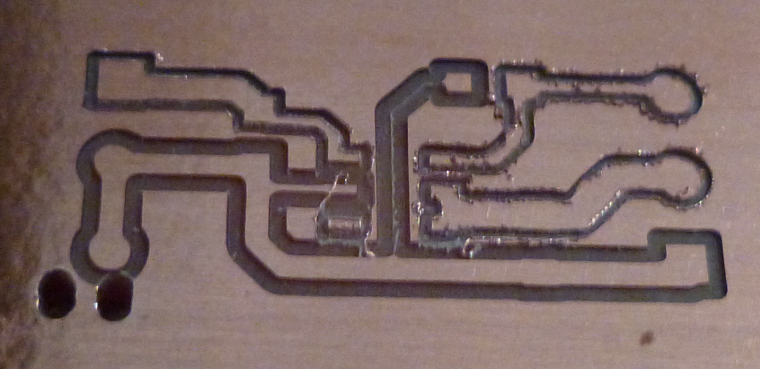
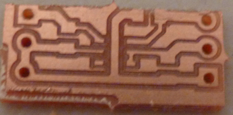
Here's my first milled PCB that's standalone:
-
I soldered on three 0805 components, but afterward I was surprised to find that all three were shorted (tested using a cotinuity meter):
I thought I had been reasonably careful soldering them on too, so I'm not sure what went wrong.Scratch that. I found that the faults were measurement error. Re-testing it, it checks out 100%. No shorts. :)
-
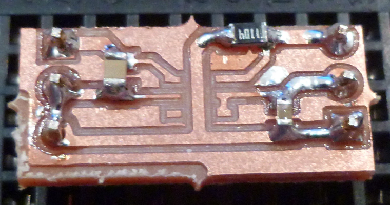
This morning I soldered on the load switch IC. I then tested the circuit, and voilà, it works. :)
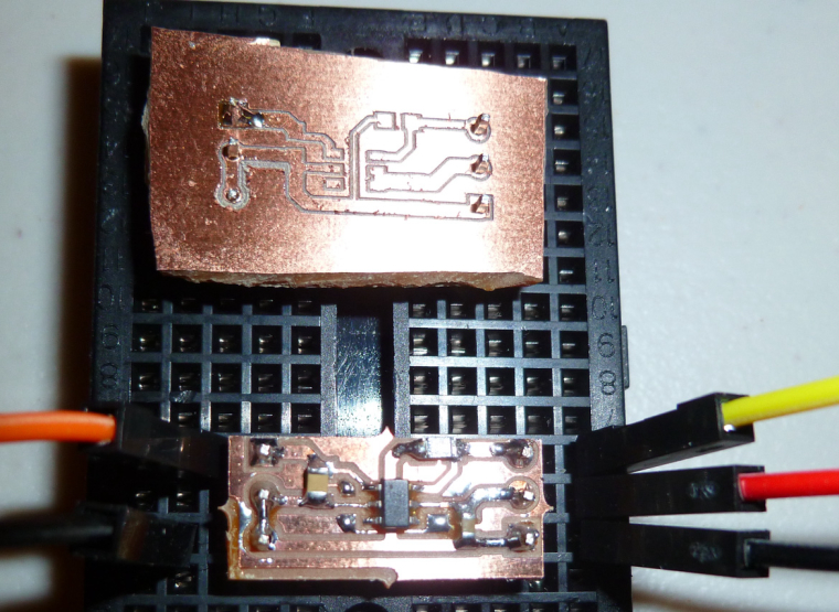
Fortunately, solder doesn't seem attracted to the PCB substrate, and it behaves like solder mask. :)By the way, the PCB above it I cut out with tin snips, which is very fast and avoids all the dust generated if using the CNC to route the board outline to release it from the copper clad blank. The result looks crude, but that doesn't matter if it's just for prototyping.
-
@executivul I noticed this youtube video, where they use mineral oil for dust containment:
https://www.youtube.com/watch?v=d9kfzRycQzEHave you tried that?