Everything nRF52840


  • @NeverDie thanks for the reply i hope to try them in the future. Best option is definitely something like BT840X or another nrf52840 or 32 with PA/LNA module it needs to be implemented with a code. i found this https://devzone.nordicsemi.com/nordic/nordic-blog/b/blog/posts/pa-lna-support-in-s132 in nordic forums but im not sure how it can be implemented into an arduino environment.
    I actually added this code to an arduino sketch and it compiled without an issue but I cant tell if it will work without having a module with PA.


  • @NeverDie also according to this post when TX/RX pins are defined softdevice handles them automatically. https://devzone.nordicsemi.com/f/nordic-q-a/40504/nrf52840-and-pa
    But if you have more control in your FEM like in BT840X with SKY66112 you need to control 2-3 more pins in your code. nRF24 modules mostly use RFX2401C its quite simple with only TX/RX pins and it works quite well may be it will pair nicely with nrf52 modules only if we could configure the code for arduino.


  • I also designed this 2 layer breakout board with a much bigger inverted F antenna design for the nrf52840, ive put BT840 to compare the antenna size. (still needs some touch ups here and there)
    Capture98.JPG
    bottom layer has a good ground layer for the antenna and i believe its going to perform better but just to be sure theres a SMA option for external antenna aswell which can be selected with the 0 ohm resistor.
    nordic specialist approved it and i will probably give it a try just to compare the antenna performance. My only concern is how hard soldering is going to be. if you noticed i removed the pins who are next to each other(i left some because they are mandatory like d+ - swclk etc..) and left the diagonal ones in order to reduce the chance of possible solder bridges. as you can see from the picture there are reports about solder bridges detected with expensive xray machines which i dont have 🙂 so, fewer the pin count less probability for failure.
    pastedimage1562114011660v1.png-640x480.png

    on the other hand ebyte nrf52840 e73 modules even with the bottom pads are really easy to solder without a probability to bridge anything and cause issues because bottom pad to pad distance is very generous, im really happy with that.
    IMG_3229.JPG


  • Hero Member

    @orhanyor Beautiful work, but how exactly do you manage to solder it? I wouldn't know how to even align it properly without some sort of jig to plunk the nRF52840 down. I'm not sure that even a surgeon at the top of his game would have the needed manual dexterity. There must be some tricks to doing this right that the module makers use. I'd think you'd have to get at least reasonably close in the first place for the surface tension of the melted lead to pull things into place.


  • @NeverDie soldering bottom/non visible parts needs at least some sort of reflow oven to make sure they melt and make connection. checking for bridges tho is impossible with microscope etc because they are under the chip. diagonal pin pitch is at around 0.55 and the ones on the same row are at 0.5 which is normal qfn package. if you can solder qfn package this is not a problem but the hardest thing is inability of inspection at hobbyist level 🙂
    aligning is very simple, you just need to have correct courtyard printed on the silk layer of the pcb for the chip/module so when you place the chip/module on to the pcb, it needs to sit exactly on top of the courtyard drawing on the silk layer then you know your pads are exactly where they need to be.
    sadly tho bigger parts like these modules cant benefit from the surface tension force is not enough to pull the weight but then again its very hard to misplace them especially the e73 module. raytac modules(blue one in the picture) are hard aswell they are like super tiny 🙂 heres how it is under the chip but it baked nicely and it works as expected.
    IMG_3199.jpg

    i hope to solder aQFN package aswell but im really not sure about that one :)) standard QFN with visible pads on the side is very nice i wish nrf52840 was like that.


  • Hero Member

    @orhanyor Ah, I see now.

    I wonder if you could use through-holes to gain access to the pads on the back of the module? I ended up doing that on one of my energy harvester boards to solder a ground pad that was on the back of a chip:
    https://www.openhardware.io/view/733/Buck-Energy-Harvester
    It worked, but it was a simpler case. In your case maybe you'd have to cut channels instead of holes.


  • @NeverDie yes that is definitely an option ive seen people do it with normal thru holes on those pads and it works. you might wanna pre tin the pads of the module and its good to go but good news for the E73(ebyte) module specifically none of the bottom pads are necessary for the module to work. they mapped every mandatory pin to the edge of the module which is very hobbyist friendly but of course you will have very few gpio pins to work with but still its very well thought by ebyte.
    i dont know when i will order the pcb for the nrf52840 but i will definitely report the result and the antenna performance 🙂 i also want to use this antenna for nrf24 but yea it is gonna have to wait not in a hurry atm.


  • Hero Member

    @orhanyor I'm very interested in your results. I think you may be the first to upgrade a module antenna. It might save a lot of money if cheaper modules can be used. Fanstells are pricey for their good antenna, so if your approach is just as good or even better...


  • @NeverDie price wise i think e73 modules are unbeatable they are 3.. dollar or something with the current discount in aliexpress. just for the nrf52840 Soc price in mouser is $5.5 which is still ok if theres going to be a noticeable difference in signal strength. considering much bigger ground plane and bigger antenna i expect better performance but need to test it 🙂 aside from the soc theres a low pass filter which is .30 and a crystal which is probably around .20-.30
    that blue raytac module was https://www.raytac.com/product/ins.php?index_id=24 8 or $9 which gave almost the same performance as the e73 so at that price point ive not tested it but BT840F($7) looks better and much easier to solder as the bottom pin pitch is whooping 1.5mm or so.. you can park a truck between those pins :))


  • Hero Member

    To free up this thread for its primary purpose, I just now started a new thread for anyone wanting to continue the wristwatch topic: https://forum.mysensors.org/topic/10917/wristwatches-that-invite-development


  • Today i thoroughly tested nrf52840 modules that i have(2 with ceramic antenna and 2 with ipex connector external antenna) all modules were set to max (+8 dBm) TX power and my observation was kinda disappointing. Setting up services, characteristics etc is fun and all but signal strength is disappointing. I tried ceramic to ceramic, ipex to ipex, ceramic to ipex and ipex to ceramic none of them stood out they gave the same performance. As soon as i put the module in a plastic container or theres more than 1 wall in between packets become unreliable and they just keep dropping, connection slows down etc it just doesnt have enough power whereas nrf24l01 with pa module is rocking even if theres like 10 brick walls in between its not even a competition. I dont think its an antenna problem because it doest get any better than ipex connector so the only option is to add some front end module. There are many options for FEM with different capabilities and functions but I will try to add RFX2401C because im familiar with it and its fairly simple. It is controlled with RX, TX pins but im not really sure how to implement it to a code.
    seems like softdevice has a support FEMs but its a question if its gonna work in arduino environment 🙂 Gotta try and see..

    https://devzone.nordicsemi.com/nordic/nordic-blog/b/blog/posts/pa-lna-support-in-s132

    also in nordics front page you can see they released a FEM for nrf52 and nrf53's its called nRF21540
    quoting from the product page
    https://www.nordicsemi.com/News/2019/12/Nordic-samples-nRF21540-RF-Front-End-Module
    "The nRF21540 RF Front End Module is a range extender optimized to boost the link budget of Nordic’s nRF52 and nRF53 Series advanced multiprotocol wireless SoCs. When combined with an nRF52 Series SoC, the nRF21540 RF FEM’s +21 dBm TX output power and 13 dB RX gain ensure a superior link budget for up to 16x range extension"
    so that kinda proves my point connection is somewhat weak and it needs a FEM any kind to at least bump the power to around 20dBm and it will all be good and usable.
    And keep in mind nrf52840 has the most power of all with max +8dBm power, 52832 has 4 and their new workhorse dual processor nrf5340 comes with +3dBm power so probably thats why they are pushing nRF21540 forward to ensure best possible connection.


  • Hero Member

    @orhanyor Yes, that's been more or less my experience as well for modules without FEM and/or good antennas. At the very least you want a gateway with a good PA and LNA and antenna. At least for me the best module I tested was the Fanstel BT840X module, which unfortunately has a high price that hasn't come down, and it's not particularly small either. If you have a BT840X/BT840XE on both ends of the link, then you probably won't experience any meaningful connection issues in, say, a 4000sf house built using typical sticks and bricks construction, which is what I tested in.

    That's why for anything needing guaranteed good range where size doesn't matter, like a leak detector, I use inexpensive LoRa modules instead. In contrast, the area where nRF2840 really shines the most is in remote controls, because it can be configured to very efficiently listen for inbound packets using just battery power for a very long time and with no perceivable latency. Thats due to its tight integration with the mcu and shared memory and the nifty PLC, not to mention the 2mbps datarate. It'd be a lot harder to do that with LoRa, which has none of that.


  • @NeverDie Well BT840X has built in FEM SKY66112 if im not mistaken, thats why you are getting good results but how did you make it work in the code. Because for TX and RX you need to tell the NRF when to listen and when to transmit so the FEM can flip switches inside and work its magic.
    Tomorrow i will try a remote application where client transmits analog read data every 50ms and reports it to the peripheral device, i will put it in a plastic box and wrap my hand around it and see how many packets it will drop tho im really skeptical after today.


  • Hero Member

    @orhanyor said in Everything nRF52840:

    how did you make it work in the code

    IIRC, it's in the datasheet. It is your code which has to flip the switches before and after a Tx or Rx. The nRF52 itself doesn't know the FEM even exists. Think of it as an aftermarket bolt-on, which is what it really is.


  • @orhanyor Your breakout board from the E73 board looks really nice. Is this something you have for sale somewhere? Would you considering selling any extra bare pcbs?


  • @Jon-Raymond selling them was not my intention but i have around 8 bare pcbs and 2 built ones. i can fix you up with one of those if you want to or i can cook totally brand new one up to you.


  • @orhanyor I'd be interested in a couple bare pcbs as I have all the components. It would save me some time rolling my own and waiting for the Chinese pcb supply chain to sort itself out.


  • i just gave this pcb to a production, it has nrf52840 and pa/lna module, 3v3 LDO on it, practically a stand alone board with nrf52. i did not include a battery connector or charger because its for prototyping. i copied the front end part from my nrf24 modules so if i can solder it should work smoothly. tho this aQFN footprint looks very intimidating 🙂 some of the tracks and gaps are at the manufacturers design capability tolerance limits so lets see if they gonna accept it.
    Caapture.JPG


  • @orhanyor Yes that aQFN footprint does look daunting. Do you have a special paste layer for the center pad that limits the paste? I've seen issues where too much paste on the ground pad will actually float the chip off the pin connections.


  • @orhanyor AFAIU you're going to solder it manually, right? Will you use stencil or are you going to presoak pads? For the stencil it might be also reasonable to order a custom PCB pallet which may help to precisely align the board to the stencil. Similarly, another pallet may help to place the chip right into the center. It will be very interesting to hear from you how it went. Wish you best of luck!

    I've ordered some boards with nRF52840/nRF52833, but also had to ask for assembly for exactly this reason. The PCBWay did machine soldering of the aQFN chip, and the rest were soldered manually.

    By the way, the PCB price were raised two times: first, for 5 mil tolerance (the board uses NFC so I was unable to route antenna differently), and second, for ENIG finish because of the aQFN-73 package (the factory insisted on it in order to avoid soldering issues). I still have no room for the RESET, but perhaps I need to go your way and drop some unnecessary pins - that's nice idea.


  • @Jon-Raymond exactly too much in the middle will raise it and bam you have a failed board 🙂
    @Mishka its a wise choice to ask for assembly because of the reasons you mentioned. ENIG is kinda mentioned everywhere for this aQFN footprint otherwise surface might not be even for every single pin and it will result in failed soldering BUT i still went with HASL just to prove them wrong :))
    capped via service is expensive so i just went through every single pin to examine and decide if i really need it or is it necessary for it to work and spaced them out as much as i can. i still got plenty, 3 analog pins, 9 high speed digital pins and rest is low frequency pins which are not recommended for high speed operations. it can interfere with the bluetooth signal. nordic specialist approved the design so if everything goes well it should work.
    my only worry was the at the bottom side XC1 XC2 pins you can see they are really close to each other i think it was 5 mil but still it was in the capabilities so it went through. i ll see how it goes its gonna be interesting.
    and yes i use stencil and a reflow oven.
    how do you like the antenna performance of the nrf52840? sadly it doesnt meet my requirements so im trying this pa lna method to see if i can make it work.


  • @orhanyor said in Everything nRF52840:

    BUT i still went with HASL just to prove them wrong :))

    I'll be not too wrong if say that literally everybody out there is waiting for the result 🙂

    capped via service is expensive so i just went through every single pin to examine and decide if i really need it or is it necessary for it to work and spaced them out as much as i can...
    nordic specialist approved the design so if everything goes well it should work.

    Yeah, HDI is too expensive for small batches. I'm just wondering how Adafruit managed to make those boards at that price. As to me the only reasonable explanation is that they produce thousands of them.

    my only worry was the at the bottom side XC1 XC2 pins you can see they are really close to each other i think it was 5 mil but still it was in the capabilities so it went through. i ll see how it goes its gonna be interesting.

    You might want drop the P0.26 GPIO I think.

    how do you like the antenna performance of the nrf52840? sadly it doesnt meet my requirements so im trying this pa lna method to see if i can make it work.

    IMHO the SoC itself is fantastic. Unfortunately, so far the only boards I have on hands are a couple of those E73 by CDEBYTE - just received them few days ago, but still had no time for them. Also, a number of nrf52833 based Raybeacons are stuck in fabrication. They're not about long range though - the board has low-performance zero clearance antenna.

    The built-in 8dBm TX amplifier is a great add-on. It comes at cost of higher current consumption, of course, so it's subject of proper battery selection for the application. An external 20dBm amplifier may require up to 150mA which will drain battery like a hog. IMHO for the cases when you need it really long a directional antenna is must.

    On the other hand, if you have to have good coverage in the center of a building it might be reasonable to stick with an amplifier. But while you're waiting for the boards, I'd suggest to give a second try to your IPEX modules with this simple DIY biquad antenna: https://martybugs.net/wireless/biquad/. It's very easy to build and promises to add more than 10dBi to your link budget. I remember I used it to feed a pair of 1m dishes (i.e. about +25dBi more) for long range wifi - worked like a charm.

    Another interesting option might be a phased array antenna. The active array will add up about 10-15dBi which is perfectly aligned to peer direction. Not sure will it be any affordable though. A passive array might be much easier to implement in PCB, but you have to align it manually.


  • @Mishka i was looking at that long range support of nrf52840 by lowering the data rate to 500kbps or 125 kbps you gain a significant amount of range like 4 fold but it requires a coded PHY which is not available in arduino environment at least not that i know of. adafruit marked it in their to do list but know knows when they gonna implement it probably thats why nrf24's make a significant difference in signal strength when you lower the data rate to 250kbps.
    Yes that amplifier draws quite abit of current i think it was up to 350ma when tx is on but ofc it is not on all the time so but still its not for everyone.
    i will look into that antenna you mentioned while im waiting for the pcbs thank you for the suggestion!
    antenna that i used in the pcb is this one: i read its better than chip antennas but ofc at a much bigger footprint
    http://www.ti.com/lit/an/swru120d/swru120d.pdf


  • Hardware Contributor

    @orhanyor I can confirm this pcb antenna works well. I used it with 52832 a while ago. You'll certainly need to tune it to get the exact target freq though, usually to do on each new pcb design&shape (so it's not shifted too much compared to your others nodes), but it's a good antenna, easy to use, resistant to detuning. This is the recommended ant by TI for 2.4ghz.
    Here I just have one bt840xe on custom gw (dual band gw, using BLE for 2.4ghz) with good external ant, it has very good range. I didn't design the 52840+PA because I preferred to have ce/fcc for PA, and for one device only, it wasn't worth the shot. For others nodes, I don't need PA, or prefer mysensors subghz for very long range.
    For a devboard, this looks nice, but depending on the target application and sensitive sensors etc, maybe adding an rf shield could help in some cases, especially as you're planning to use a power amplifier. Spectrum analyzer (or a vna) can help to check this (bad rf emissions too, passive filtering can help) and optimize range.

    good luck for your soldering 🙂


  • @scalz thanks for the input, ive seen they tune it by cutting a length from the longer end but in order to do that i need equipment which i dont have so its going to be a hit or miss 🙂 if it doesnt work well i can use SMA antenna but i think thats the least of my worries with that pcb. I like to experiment and see for myself so even if its wasted its ok 🙂


  • So, 8dBm built-in, plus 20dBm PA, plus 12dBi for the feedhorn, plus 20dBi for the dish. Add the coded PHY on top of this. Does anybody want to set a record? 😃


  • In a meanwhile, here is the nRF52840 range test with Johanson 2450AT18D0100 chip-antenna and SAFFB2G45MA0F0A 1dB attenuator
    the nRF9160 range test: https://www.youtube.com/watch?v=p1_0OAlTcuY (spoiler - 14 km).


  • Hardware Contributor

    @Mishka said in Everything nRF52840:

    In a meanwhile, here is the nRF52840 range test with Johanson 2450AT18D0100 chip-antenna and SAFFB2G45MA0F0A 1dB attenuator: https://www.youtube.com/watch?v=p1_0OAlTcuY (spoiler - 14 km).

    typo?? from the video, it seems to be nRF9160


  • @scalz No. The nRF9160 DK has nRF52840 on board.


  • Hardware Contributor

    @Mishka I meant nrf52840 does not do LTE/NB-IOT. 52840 is used as controller/bridge to bluetooth (14km range isn't for bluetooth). but yes their NB-IOT sip looks nice


  • @scalz You're right. They did NB-IoT, not BLE. Shame on me!


  • Hardware Contributor

    @Mishka bah no shame, enthousiasm is good thing 😉


  • @scalz Yeah, next time I just have not read, but watch the video.

    My impression was that the snow coating acted like a mirror thus greatly extending the range. But I admit 14 km is ridiculous. So sounds like a challenge 🙂


  • Hero Member

    Adafruit now has an alpha release nRF52840 offering in a BBC microbit form factor:
    https://www.adafruit.com/clue

    alt text

    The listing says it's programmable from the Arduino IDE.

    The original micro:bit seems locked in time, with no official mcu upgrades from micro:bit itself, but nonetheless by the end of 2018 over two million micro:bits had been distributed globally. Pretty amazing for such a minimalist, barebones platform.


  • @NeverDie Ya Adafruit's Clue looks great. I just wish they would have added one more button to the front so up/down/select could be used for a menu system on the display.


  • Hero Member

    @Jon-Raymond said in Everything nRF52840:

    @NeverDie Ya Adafruit's Clue looks great. I just wish they would have added one more button to the front so up/down/select could be used for a menu system on the display.

    Maybe you could program one of pads #0, #1, or #2 to be a capacitive touch equivalent of the extra button you wish it had?


  • @NeverDie Yes that is a good option or use the accelerometer to sense an input.


  • Hero Member

    A datasheet for the new nRF5340 is now available: https://infocenter.nordicsemi.com/pdf/nRF5340_OPS_v0.5.1.pdf

    It has some improvements, but some of its competition seems to be much lower power.


  • Reading all of this, I think I made a mistake buying the e73-2G4M08S1C and a Deb board. I doubt I have the capabilities to solder this board properly. Since I have no experience designing boards, is there any simple breakout board design available I can order from pcbway so I can at least solder the outer pins?
    The only board I found was this one:
    https://www.openhardware.io/view/745/Light-and-shock-sensor-or-nRF52840-or-MySensors-or-ZigBee


  • Hero Member


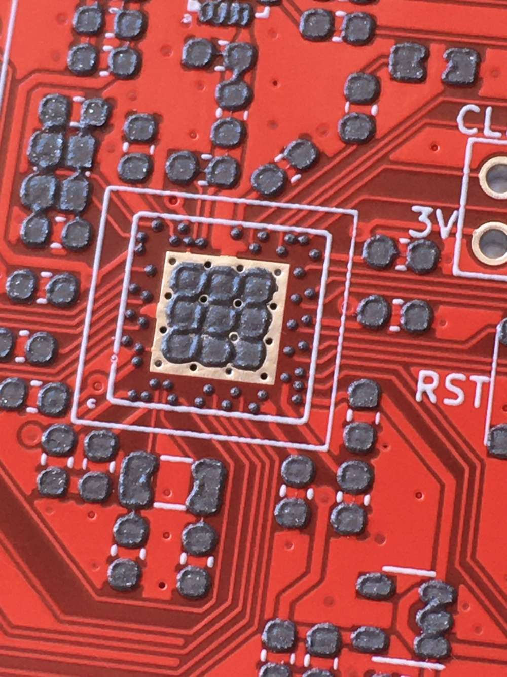
  • @NeverDie doh! I glossed over that one and just assumed it wasn't possible for me due to the pads. Now on 2nd viewing I see that the inner pads are actually through holes, so I can solder them from the other side 🙂
    Thanks! Has anyone tried that one and has any tips?


  • I would also be interested in hearing tips for this type of soldering (thru-hole to pads)
    I tried the thru-hole method with the LGA pads on the back of an BT832. It wasn't very successful, I was only able to get one of the 5 holes in my pattern to connect. These look larger and more widely spaced, so it probably works better.


  • Hero Member

    @nagelc Not sure, but here's a guess: maybe generously tinning some braided wire so as to wick up the solder, dipping it in lots of flux, and then feeding it through the hole? Then when you apply heat from a soldering iron hopefully enough of the wicked solder would melt onto the pad to make a connection.

    However, I presume the better way would be to apply solder paste on the pads before sticking on the module and then reflow it in an oven.


  • @NeverDie Of course the oven is the way it is meant to be done.
    I have the oven waiting to convert, but that's still ahead on my project list : )


  • Hi everyone,
    I'm a bit a newbie in hardware and need your help. I'm a PHD student and I actually work on ZigBee networks. For a POC, I need to have an hardware device able to capture and send ZigBee messages from a "true" physical device. (An old philips Hue or maybe an Ikea smartbulb for example - normally, 2.4GHz).
    The idea is to make a false ZigBee Gateway to work on the secrurity of the enrolment in ZigBee 3.0 within software.
    My issue is that I'm unfortunately a bit newbie in on-board programming and thus can't be sure if it's feasible and if it's really complicated or not. I'm posting my message here because the nrf52840 seems to fit my needs with a ZigBee compatibilty.
    Thanks by advance for your answers !


  • Hardware Contributor

    hello @TruiteCendrée 😁

    yes this is possible with nrf52840, but unfortunately zigbee is not compatible with mysensors. Mysensors is a software stack like zigbee is.

    I think you'll get more infos if you take a look on nordic semi forums. They have a zigbee stack for nrf52840.


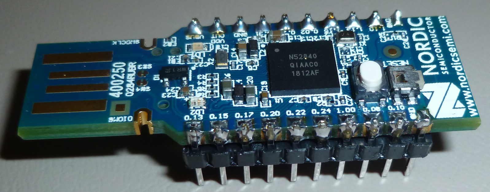
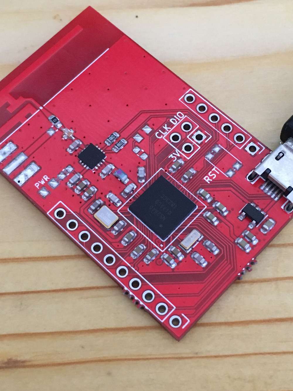
  • hey guys, i finally assembled my nrf52840 pa board. it was sitting there for quite some time but i couldn't find some spare time to get on with it but here are some experiences i had.
    i was worried about this aQFN footprint but it all went well, looks like everything is soldered correctly and i ordered my boards with cheapest HASL instead of ENIG.
    IMG_3870.JPG

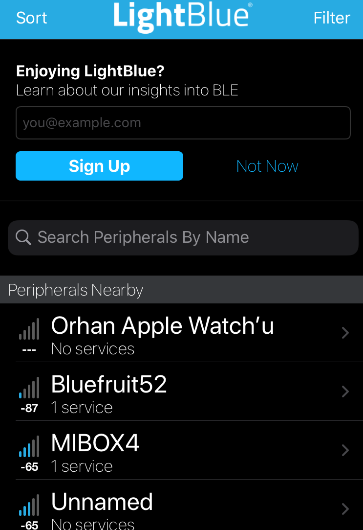
    then i uploaded the adafruit feather bootloader to test the bluetooth and it all works ok. i used my iphone 6s as a central device and im not sure if my phone has LNA or PA module inside for bluetooth so it may or may not be better if i use another module like the one i did. this connection is from my module to my phone WITHOUT PA activated at tx power max(8):
    without pa.PNG

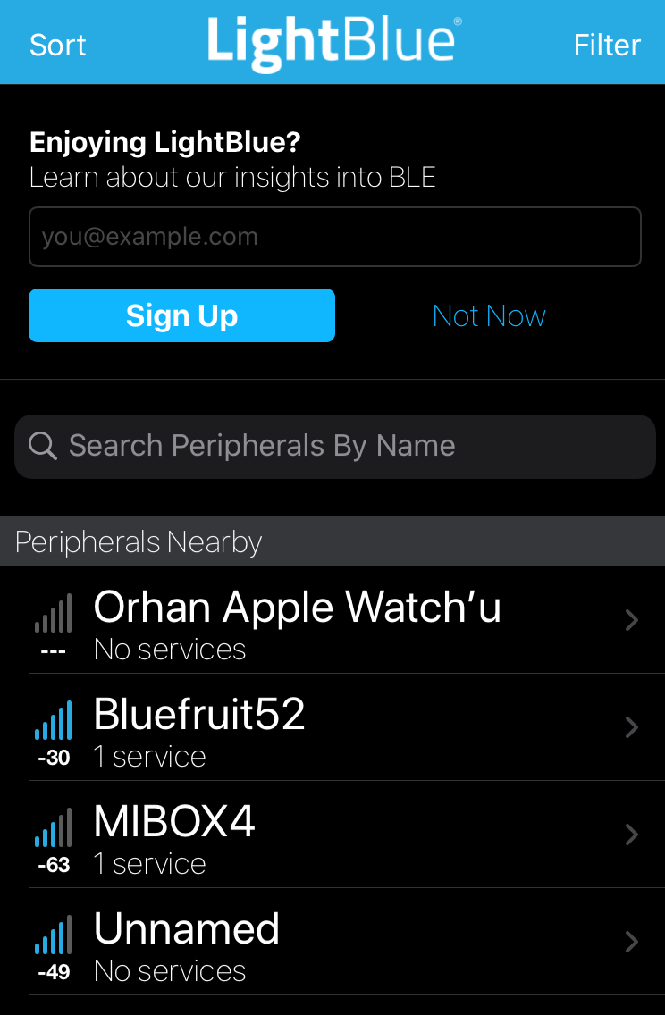
    and this is after i activate PA chip on board :

    with PA.PNG

    and this is with 3 solid walls in between at around 10 meters distance
    3 solid walls.PNG

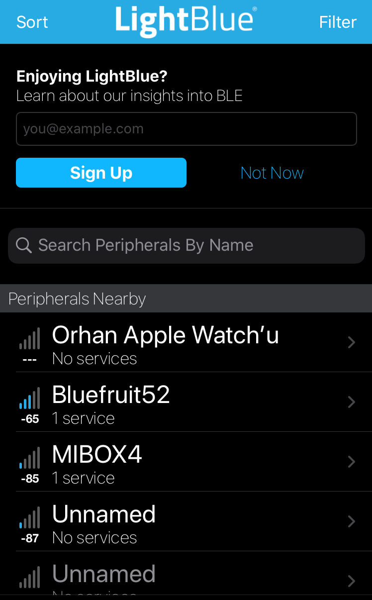
    as you can see signal strength is massively different pa bumps up the signal from -87dbm to -30dbm which is probably day and night difference.
    but with this setup you manually have to enable and disable rx and tx pins in order to keep the communication. well im not really good at coding but im going to try make the whole thing automatically because nordic already has this PA assist feature buried inside its BLE core, just gotta find a way to make it work.

    final board, forgot to add i opted to use pcb antenna but i could switch to external antenna as well i just have to reposition the 0 ohm resistor to use that SMA on the side and then results could get even better:
    IMG_3878.JPG


  • Hero Member

    @orhanyor Nice! How did you manage to do the solder paste so precisely?


  • @NeverDie i had to use stencil because i cant inspect aQFN soc from outside. as you can see every pin is at the bottom of it and they are very tiny. to make sure theres correct amount theres no other way than using stencil. to be honest i was expecting problems but it was ok 🙂


  • after abit of looking around and testing i think i made it work at least examples are quite responsive without a single disconnect. i had to add some header files and extra bit of code to every sketch so the knows how to use PA/LNA.

    static void pa_lna_assist(uint32_t gpio_pa_pin, uint32_t gpio_lna_pin)
    {
        ret_code_t err_code;
    
        static const uint32_t gpio_toggle_ch = 0;
        static const uint32_t ppi_set_ch = 0;
        static const uint32_t ppi_clr_ch = 1;
        
        // Configure SoftDevice PA/LNA assist
        ble_opt_t opt;
        memset(&opt, 0, sizeof(ble_opt_t));
        // Common PA/LNA config
        opt.common_opt.pa_lna.gpiote_ch_id  = gpio_toggle_ch;        // GPIOTE channel
        opt.common_opt.pa_lna.ppi_ch_id_clr = ppi_clr_ch;            // PPI channel for pin clearing
        opt.common_opt.pa_lna.ppi_ch_id_set = ppi_set_ch;            // PPI channel for pin setting
        // PA config
        opt.common_opt.pa_lna.pa_cfg.active_high = 1;                // Set the pin to be active high
        opt.common_opt.pa_lna.pa_cfg.enable      = 1;                // Enable toggling
        opt.common_opt.pa_lna.pa_cfg.gpio_pin    = gpio_pa_pin;      // The GPIO pin to toggle
      
        // LNA config
        opt.common_opt.pa_lna.lna_cfg.active_high  = 1;              // Set the pin to be active high
        opt.common_opt.pa_lna.lna_cfg.enable       = 1;              // Enable toggling
        opt.common_opt.pa_lna.lna_cfg.gpio_pin     = gpio_lna_pin;   // The GPIO pin to toggle
    
        err_code = sd_ble_opt_set(BLE_COMMON_OPT_PA_LNA, &opt);
        
    }
    

    in this form i like the ble, without pa not so much. theres just big down side which is nrf52840 definitely not hobbyist friendly. next time i may design a quick nrf52832 pa board (this one has regular QFN package) to test with the same setup and compare the results.


  • @NeverDie , indeed OTA is optimal, then at least the default pre-flashed bootloaded is not so bad to be able to update SW without debugger. But for development purposes the USB dongles are much cheaper than the devkit, yet lacking debug connections. I hope this pogo pin adapter can help others, as I use it to flash and even debug with Ozone on that cheap nRF52840 USB dongle.
    Link to CAD Model : https://a360.co/3jr91PD
    Also on thingiverse although thingiverse connection is not stable
    https://www.thingiverse.com/thing:3384693

    I also like platformio Arduino and would like to have the nRF52840 USB dongle supported without the softdevices, as they prevent the direct usage of the RF peripheral for custom radio.

    pogo-versions.jpg


  • Hero Member

    @wassfila Nice! Thanks for posting. There's also this one for those who want to something readymade: https://www.tindie.com/products/ElectronutLabs/pogoprog-model-c-pogo-pin-programmer-swd-2-pack/
    It looks like yours has the advantage of being self-aligning. It certainly helps a lot if you can lock it on and not have to hold it. Does yours do that already, or would it need a rubber band (or something) in addition to hold it in position?

    I've been kinda intriqued by these things: https://www.segger.com/products/debug-probes/j-link/accessories/adapters/10-pin-needle-adapter/
    because it's general purpose and you can lock them on, but the downside is that the latching holes consume a fair amount of board real estate.


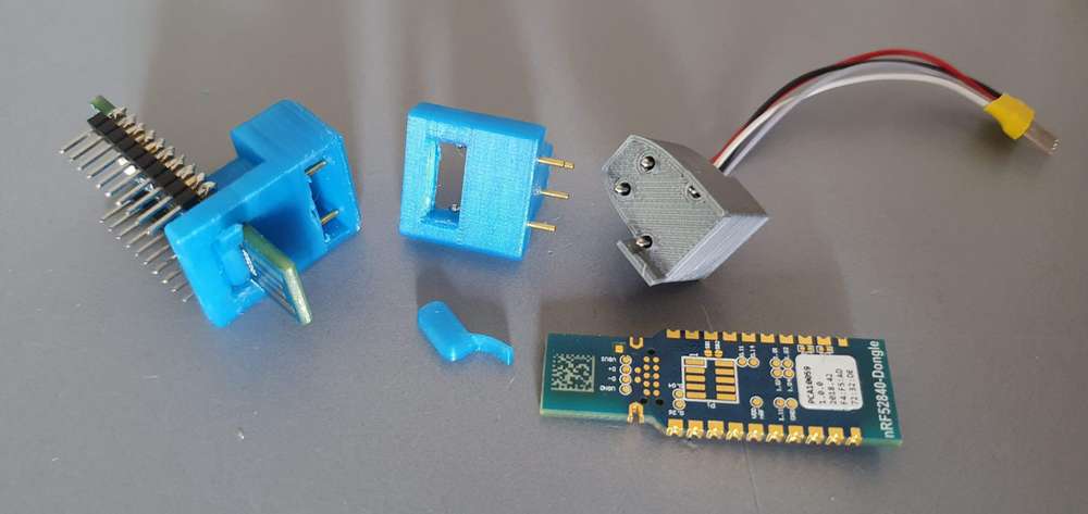
  • @NeverDie , you got it right, mine has the advantage of being self holding, which is quite an advantage if you want to debug, I tried, to debug in the past using the keyboard with only one hand, not very efficient 🙂

    As you can see, the one in the left side, is holding by itself, it does not has the cables soldered though, the one on the right is my first iteration, but the side holders are weak and broke with time.
    It is true that the fact of picking the two side points, it makes it self aligning.
    The blue versions are the newer ones, where you can slide it in with the pogo pins stretched out, and then you press it in and lock the open space in the bottom with that small blue little thingie that we see unused and free in the middle version. So no rubber band required, all is static mechanics.
    Both middle and left versions are available, the middle version requires glue to fix the pogo pins in the printed shell after being inserted the first time but makes soldering the wires on top easier. The left one has a roof holding the pogo pins but they're harder to access for soldering the debug wires in them and also printing is with slightly more debris given the complex bridging.
    One way or the other, this managed to get me a self-standing pogo pin adapter of an already existing board. Indeed if you design your own, you can think of those you linked, but if you're short of space, you can also fallback on such custom 3d printed solutions.
    This nRF52840 usb dongle is an amazingly powerful board and so cheap, that I'm confused why Nordic did not made the debug for it simpler, feels like they prefer to sell the dev kit for prototyping, but they don't know how hobbyist like to prototype on the final cheap product. I could afford 5 of them to experiment with some mesh protocols.

    So if you have access to 3d printing and would like to give it a try, I'll stay around and help if needed, also if you have improvement suggestions, I struggle with fusion360 till I get things done.


  • Hero Member

    @wassfila Nicely engineered!

    BTW, if I'm not mistaken, Adafruit's bootloader ( https://learn.adafruit.com/introducing-the-adafruit-nrf52840-feather/update-bootloader ) should work on these dongle boards as well. I suspect the way it may works is:
    0. Install the booloader as per the instructions in the link above. Thereafter,

    1. Plug the dongle into the usb port on your pc, whereupon lit's treated like a virtual hard drive.
    2. Drag the binary you want to upload to the virtual drive icon on the PC
    3. Reboot to finish, and that launches your program.

    Anyone tried it? If so, is that a correct summation?


  • @NeverDie i can speak for arduino side im not sure how it works for CircuitPython. virtual hard drive part is only true if there was a bootloader prior to update. im not sure how nordic ships their dongles but i think they dont install adafruit bootloader inside of them 🙂 so you need a fresh bootloader install and it is easy but you need jlink for that. after connecting your jlink to nrf52 open the arduino from menu find jlink for adafruit nrf52 and then just simply click install bootloader and voila it works with arduino.
    but then again that usb dongle wont work seamlessly with adafruit bootloader because im sure adafruit has different pin maps you just need to check their pins from variants file and match them on paper to the dongle so when you write your code you know which ones to use, unless theres a seperate variants file specifically made for this dongle.


Log in to reply
 

Suggested Topics

  • 87
  • 7
  • 9
  • 7
  • 10
  • 8

11
Online

11.2k
Users

11.1k
Topics

112.5k
Posts