💬 No neutral power supply/relay board for in wall switch
-
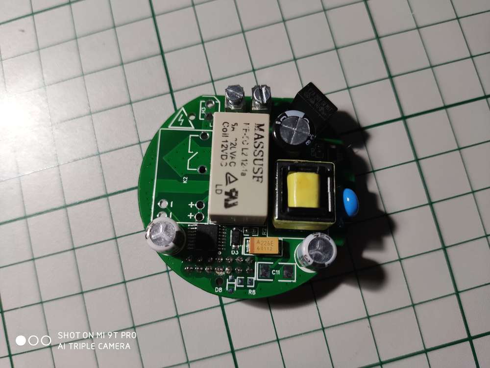
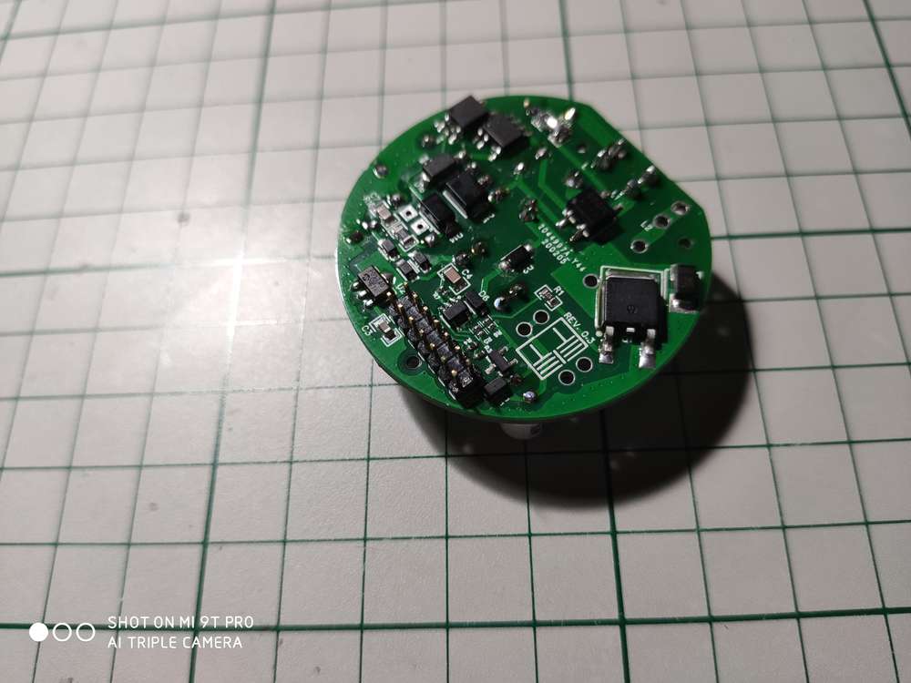
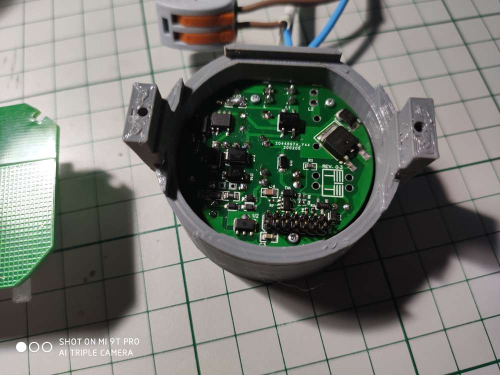
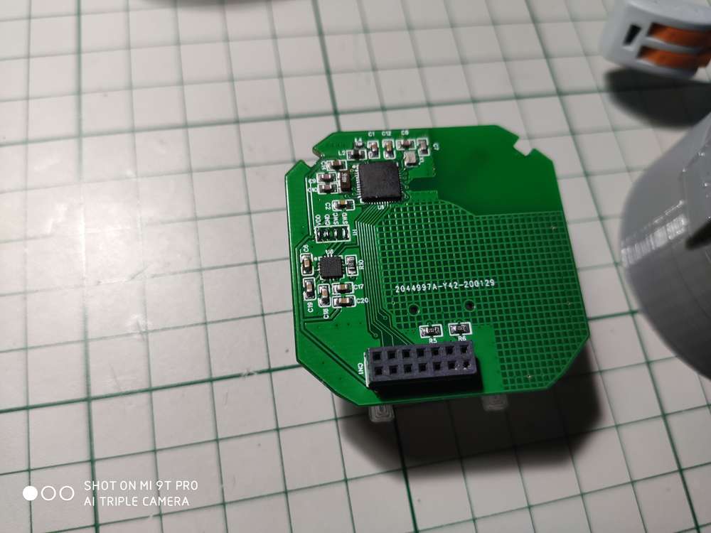
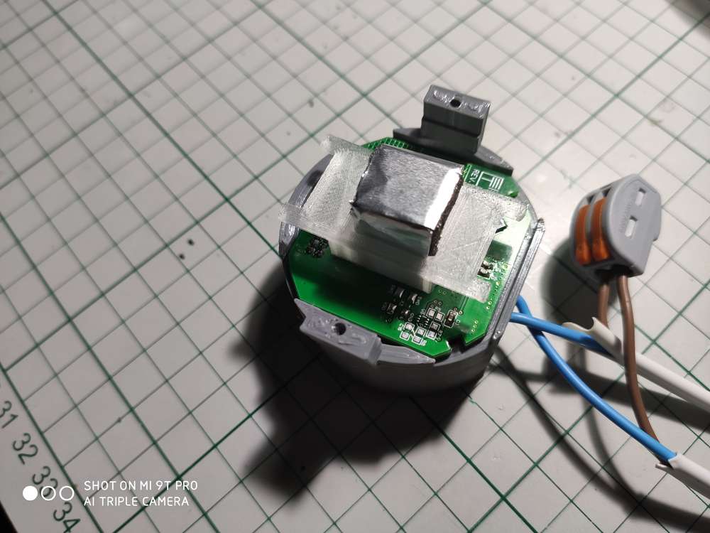
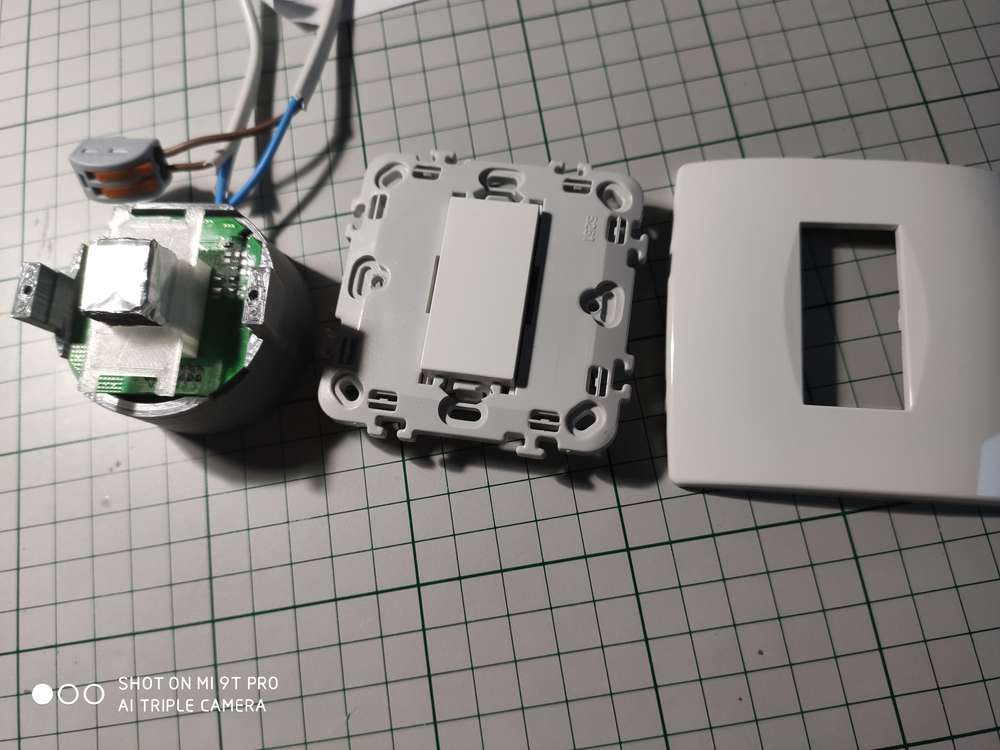
And the real product pictures now:
Short demo of touch functionality (will post later on the bluetooth mesh network functionality):
https://streamable.com/b52qb
https://streamable.com/dj3z7Sorry for the solder bridge replacing the R20 inrush current limiting resistor..that's just temporary until I get the real component :smile: . And yes, the capacitor across the bulb is still needed but it's a very small one of 0.1uF/250Vac and it should fit near the light bulb on the ceiling (only one is needed if there are two light bulbs on the same circuit).
The aluminum foil wrapped around that sponge is to "extend" the capacitive sensor so that it reaches the front plate fake plastic button. The 3d printed clear plastic around it is to hold it in place and also to spread the small leds light.
Everything is custom made except for the front plastics.
-
@mtiutiu
congrats :clap:
I'm curious, are you happy with range (I noticed you changed a bit the rf reference design routing).
I guess you use BLE mesh regarding average power consumption (which should improve range too), so rfm69+mysensors is maybe too power hungry?
Well, I think I'll try to assemble a few of your boards, this might be the first design I try here :nerd_face:
thx for sharing, I can imagine it was lot of work and time. -
@mtiutiu
congrats :clap:
I'm curious, are you happy with range (I noticed you changed a bit the rf reference design routing).
I guess you use BLE mesh regarding average power consumption (which should improve range too), so rfm69+mysensors is maybe too power hungry?
Well, I think I'll try to assemble a few of your boards, this might be the first design I try here :nerd_face:
thx for sharing, I can imagine it was lot of work and time.@scalz
Thanks.To answer your questions:
- Range is not that "big" if having multiple walls - if more than 1-2 walls things start to degrade but having more nodes in the mesh helps to overcome this. Also one can tune the number of retransmits as shown on my blog and having more relaying nodes will help a lot also. Of course my custom RF design is not perfect or that optimized. Add to that the ceramic antenna which is not that great...
- Power consumption is a plus also indeed as per node I get around 7mA x 3.3V ~ 24mW. Let's add to this the leds and touch capacitive sensor and make it 30mW on average but no more than that. I enabled the internal DC-DC converter of the MCU and add to that the fact that the nodes will stay more in RX mode hence the 6-7mA constant current draw.
- The boards are a little bit different but not much from a RF performance point of view (I'm still learning this part when it comes to PCB layout)
- The hatched ground plane differs around the capacitive pad(s) but that's because the PCB was designed initially using EasyEDA which offers "90 degree" hatches. Then I ported the PCB to KiCAD where I had to do a little trick with some polygons at 45 degree as it doesn't support hatched ground planes (not now at least or in the stable version).
I tested already both designs - the original one and the KiCAD conversion also and both are working as expected.
Yes it was lots of work and especially the power supply PCB design for which the main inspiration was the DER-622 application note from Power Integrations.
But I'm very happy with the overall result. I will update the blog with some real life videos of the whole system in action in the near future also. There will be more blog entries targeting this topic - that's for sure.
-
Yes, it's available here. The documentation is a little bit scarce I admit but if you understand Apache MyNewt and its build system it should be pretty straightforward theoretically.
I will add more details when I have the time. The code was tested and it's in production. Works without a glitch so far.
-
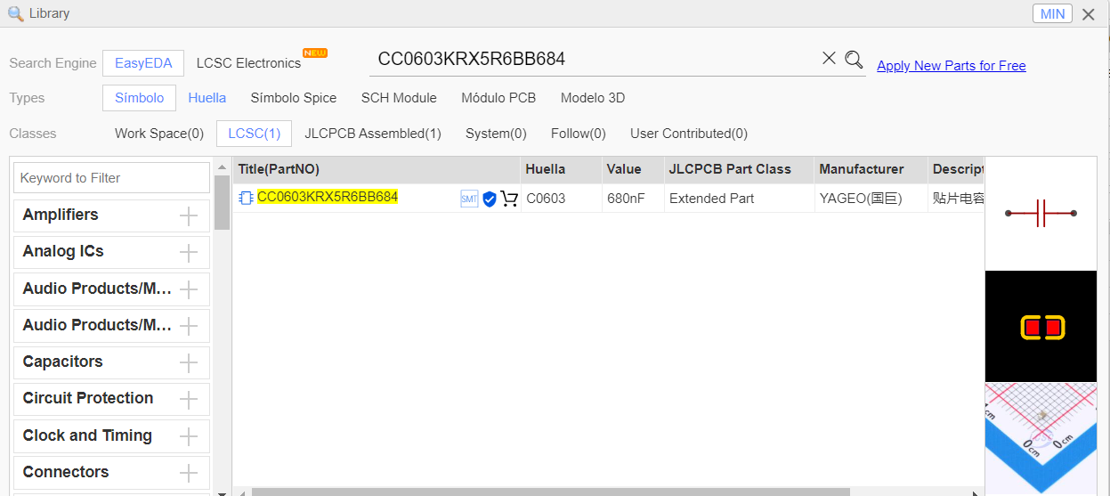
Hello,
I looked for the manufaturer part of C10 in EasyEDA Library "CC0603KRX5R6BB684" and I noted that it describes a 680nF/10V capacitor, but in the schematic it is supposed to be 100nF/50V, (CC0603KRX7R9BB104), so which is correct?
-
Hello,
I looked for the manufaturer part of C10 in EasyEDA Library "CC0603KRX5R6BB684" and I noted that it describes a 680nF/10V capacitor, but in the schematic it is supposed to be 100nF/50V, (CC0603KRX7R9BB104), so which is correct?
This post is deleted! -
The LNK364 has an internal 6.3V zener diode across BP and S so the 10V is OK, though the 50V is probably a better idea. The data sheet indicates the capacitance should be 0.1 μF (100nF). I'd recommend the latter. (It could be a typo in the EasyEDA)
-
Thanks @OldSurferDude.
I am bit newbie in circuit design, does the R20 inrush current limiting resistor must be 2W? or the 0.5W resistor in the BOM works fine?
-
I would say the 2W should be used. I say this because it would be exceptional to spec 2W and there is probably good reason to do so, though I do not know that reason.
Often times people with experience with the design reason that a different value will work. Or they find that the component doesn't mechanically fit into the modified design. (I will admit to doing this myself) I suspect that the resistor periodically is dissipating 1W (1W of tolerance). If this is the case, after many cycles, even years, the 1/2W will fail.
I will share some experience. I put 2W (12V/0.15A) into a 2W resistor. I went to pick up the board and grabbed it by the resistor and burnt the crap out of my fingers.
Overdesigning is good. Cautionary tale: Mrs. Fiorina told the printer mech designers that they make the printers too good and that they should make them cheaper. The company of which she was CEO is not doing so good today.
-
Pardon if the question is silly,
I want to use this power supply to pwer up a small mcu and some leds, but I don not know if I could draw less than what one of the notes says: "The touch sensing board including radio/mcu must not draw more than 8-10mA on average" why is that?
-
My guess is that the the leakage power captured can only supply that amount of current (at the specified voltage)
Hello! It looks like you're interested in this conversation, but you don't have an account yet.
Getting fed up of having to scroll through the same posts each visit? When you register for an account, you'll always come back to exactly where you were before, and choose to be notified of new replies (either via email, or push notification). You'll also be able to save bookmarks and upvote posts to show your appreciation to other community members.
With your input, this post could be even better 💗
Register Login