My own board (50mm x 30mm)
-
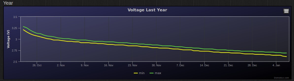
Battery-monitoring
The capacitor between AREF and ground (C3 in my schematic) is not to pull that pin to ground, but to stabilise this reference. Not strickly needed I think, but I prefer it since my sensors will live in a "noisy" environment.The code to check the level of VCC using the internal 1.1V reference is found here:
http://provideyourown.com/2012/secret-arduino-voltmeter-measure-battery-voltage/The error of 10% is something I can live with, since I need to be able to measure the supply-voltage and monitor it. It does not need to be super exact, since I plan to replace the batteries when I see levels around 2.2V. I'm mostly interested in the trend graph.
When using a DC stepup converter, you will of course need to use a pin to measure the original battery level, because the step up will make VCC always 3V3. I like your idea of dual use, so I will implement the pins to hold a voltage divider anyway. It is indeed a good use of PCB space.
I also ordered some step up converters (from Aliexpress) and I will measure them once I get them. Not all China stepups are crap it seems (as far as I read on various websites).
LED
As for the LEDs, I have only 1 LED on my boards. The LED blinks very shortly (5ms) every minute to show that a message is sent. It flashes three times if there is an error. So no need to have two leds. It is also the same LED that is flashed by the bootrom (I'm compiled nmy own version of Optiboot to used pin 14 of the atmega328. On a atmega1284p I use pin 1. This is personal preference.I checked your schematic. You will need to change the value of C1 (it is now 22pF, will need to be 100nF).
I will need to read the datasheet of the atmega328 again to understand the exact use of AREF. I'm not sure that pulling this to VCC is a good idea.
It seems you have removed the crystal and capacitors and plan to use the internal oscillator, I did this as well. Works most of the time, but uploading of sketches can give transmission errors of you go above 57K6 baud. Better to transmit at 36Kbit then (needs a change in the BOARDS.TXT file of Arduino IDE). Slower, but not a problem if you do not plan to change the sketch every 5 minutes.
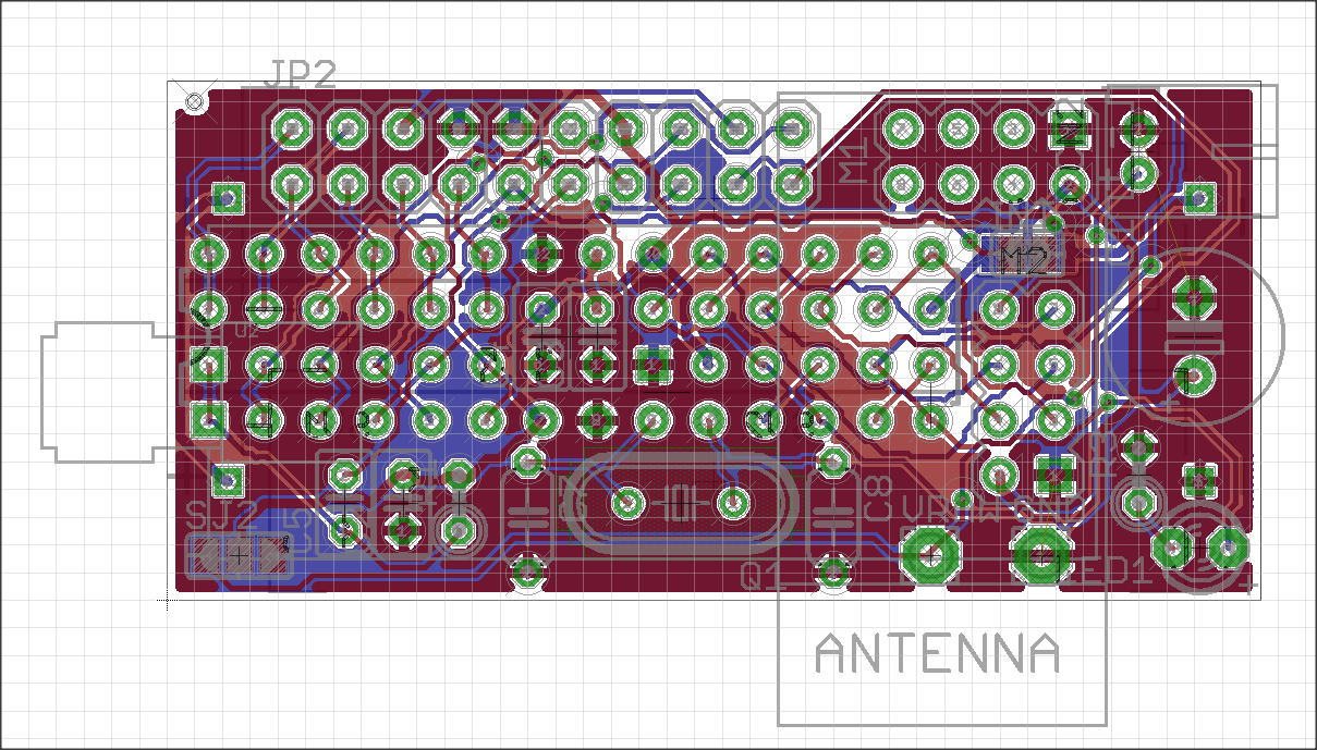
Here is a preview of my new board:
It will be able to work both as a repeater (NRF24 with antenna) as well as a normal sensor board (small NRF24). The voltage divider on A0 is not yet implemented here. Still some empty spaces :-)
@GertSanders said:
It seems you have removed the crystal and capacitors and plan to use the internal oscillator, I did this as well. Works most of the time, but uploading of sketches can give transmission errors of you go above 57K6 baud. Better to transmit at 36Kbit then (needs a change in the BOARDS.TXT file of Arduino IDE)
76K8 baud works better than 57K6 (division from 8 MHz has less error), and there are Optiboot variants which support it (with theBOARDS.TXT change you mention). Or 38K4 baud (half that) as you suggest, which is no more timing accurate than 76K8 but by being slower still may give more margin for sloppy edges or the like - if needed.
-
Hi GertSanders,
After ordered and make 3 of 50mm x 30mm board with success. Now I ordered the AC Capable 50mm x 50mm board. I try to read the schema and I have some question. If I want to use this board with only 2 AAA battery, Do I need to use AMS1117? and witch jumper do I need to close? It is optional to use AT24C ?
Thank you for your help
-
@Carl-H To use the board with AA batteries you do NOT need to place the AMS1117. But you will need to short the jumper "BAT" which you will find on the same surface as the AMS1117 if you want to feed the NRF24 with the same power.
The batteries are connected to the Vcc power line. The NRF24 is connected to the 3V3 power line. There is no interconnection, unless you use the AMS1117 or you short the jumper "BAT".The AT24C's are optional. If you do plan to use them, you will also need to place the I2C pull resistors and you will need to short the jumpers RSCL and RSDA. These two jumpers connect the pull-up resistors to the SCL and SDA lines.
If you use a sensor connected to the pins SCL/SDA of the extension connector you sometimes have no need for pull-ups as the sensor itself has them.
The jumpers SCL-SDA and SDA-SCL are there to allow switching the signals of the SCL/SDA pins on the extension connector. The jumper closest to the board edge is for the pin on the very edge of the connector, the jumper close to the ATSHA is for the second pin. Without shorting these two jumpers, the pins on the extension connector have no function.
Some sensor-boards have a SDA-SCL-GND-3V3 connector, others have a SCL-SDA-GND-3V3 pattern. The jumpers are there to be able to use both types.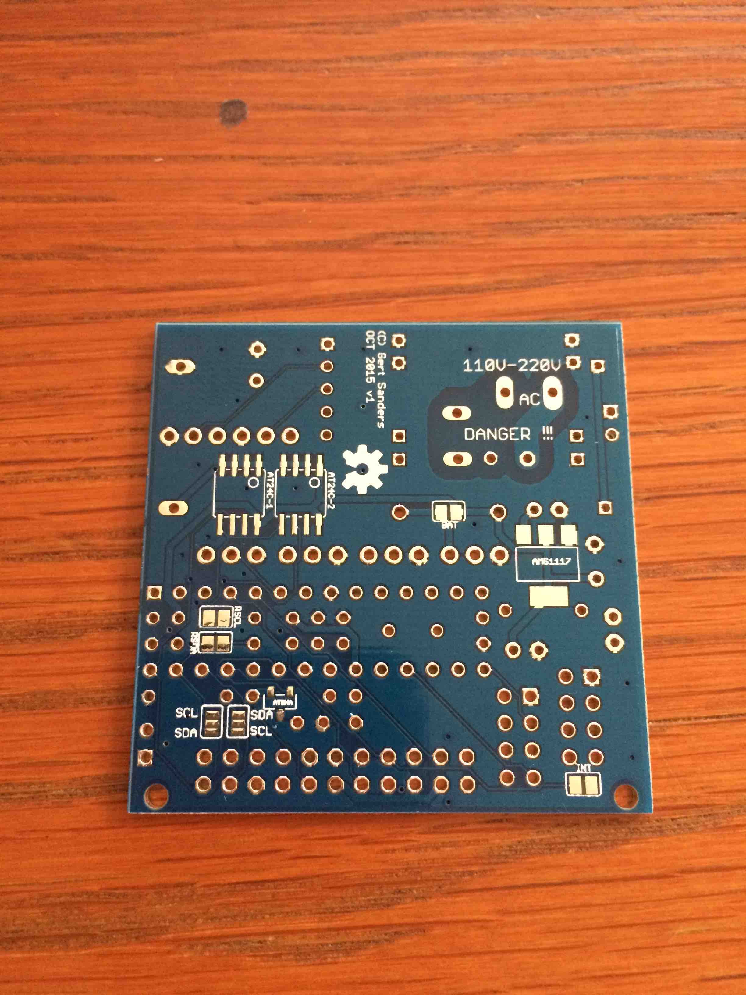
-
@Carl-H It is part of the expansion connector.
I added more info on the OpenHardware.io site.
-
Ok my boards arrived from DirtyPCB.
A couple of questions:-1.I am not using NR2 (The radio socket that protrudes),Also i am using the internal osc and not the xtal.
So can i leave out C9,NR2 Socket,C5,C6,Xtal ?
2.What are C2,C3 doing.
The socket for the cpu i have fitted will not let me squeeze them in.Should i solder them in underneath or can they be left out?
-
@mtucker
-
Yes you are right about leaving out these components, but if you use NR1 i should leave out C8 and keep C9 (mount the decouple C's as close to the decouple component as possible)
-
these components are for decoupling the uP. You can mount them at the bottom, do not leave the out.
I used a tip from earlier in this forum thread for gaining a little bit more space when using these
Cheerz
-
-
@BartE answered perfectly. You can leave out C5,C6 and XTAL if you use the internal oscillator. C9 is for the NRF24, no matter if you use NR1 or nR2 socket. And yes, you only need 1 socket, so if you use NR1, no need to add NR2 (and vice versa).
Socket NR2 is for the longer (and power amplified) radio with external antenna, NR1 was intended for the standard NRF24L01+ with PCB antenna.
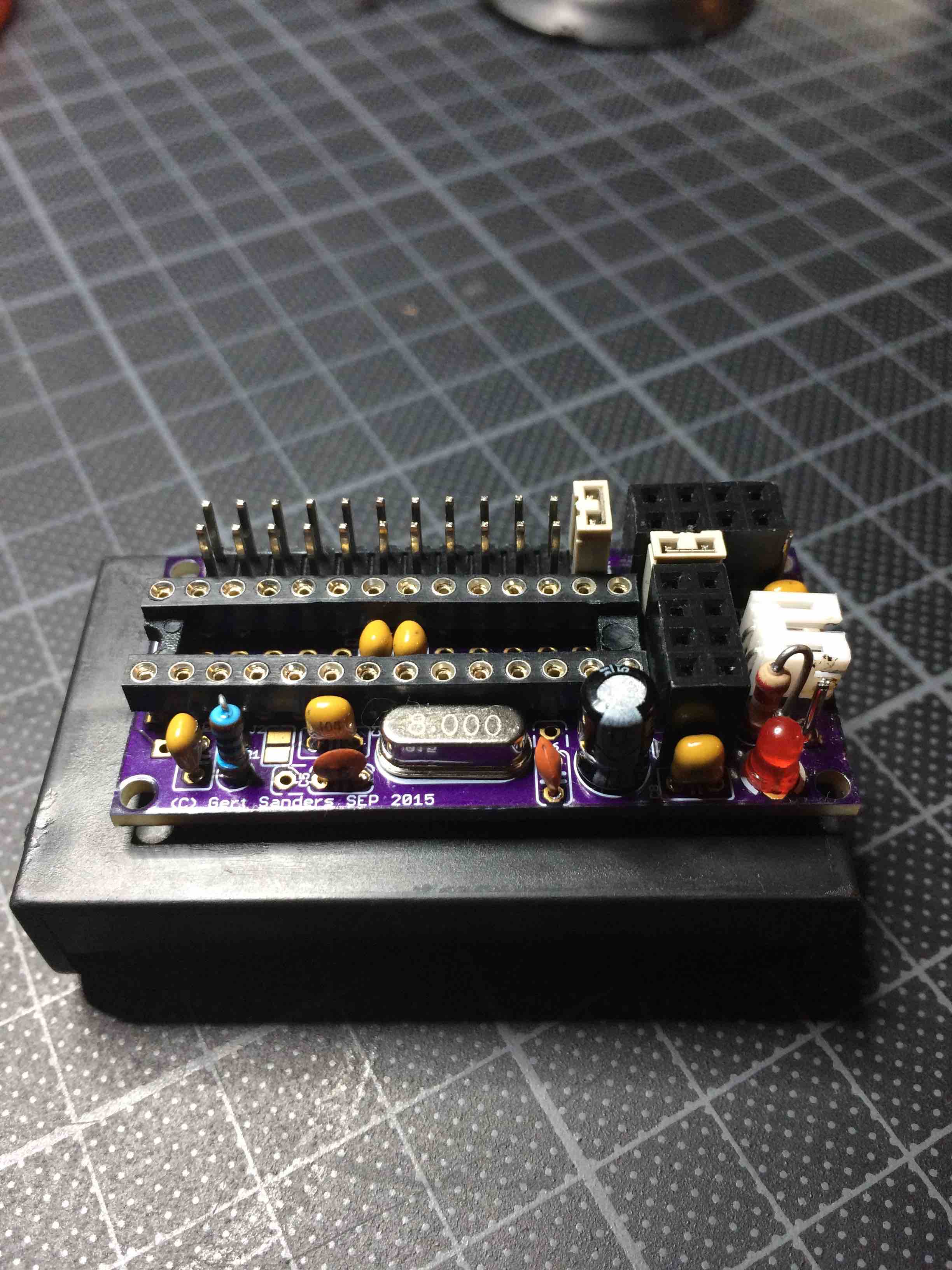
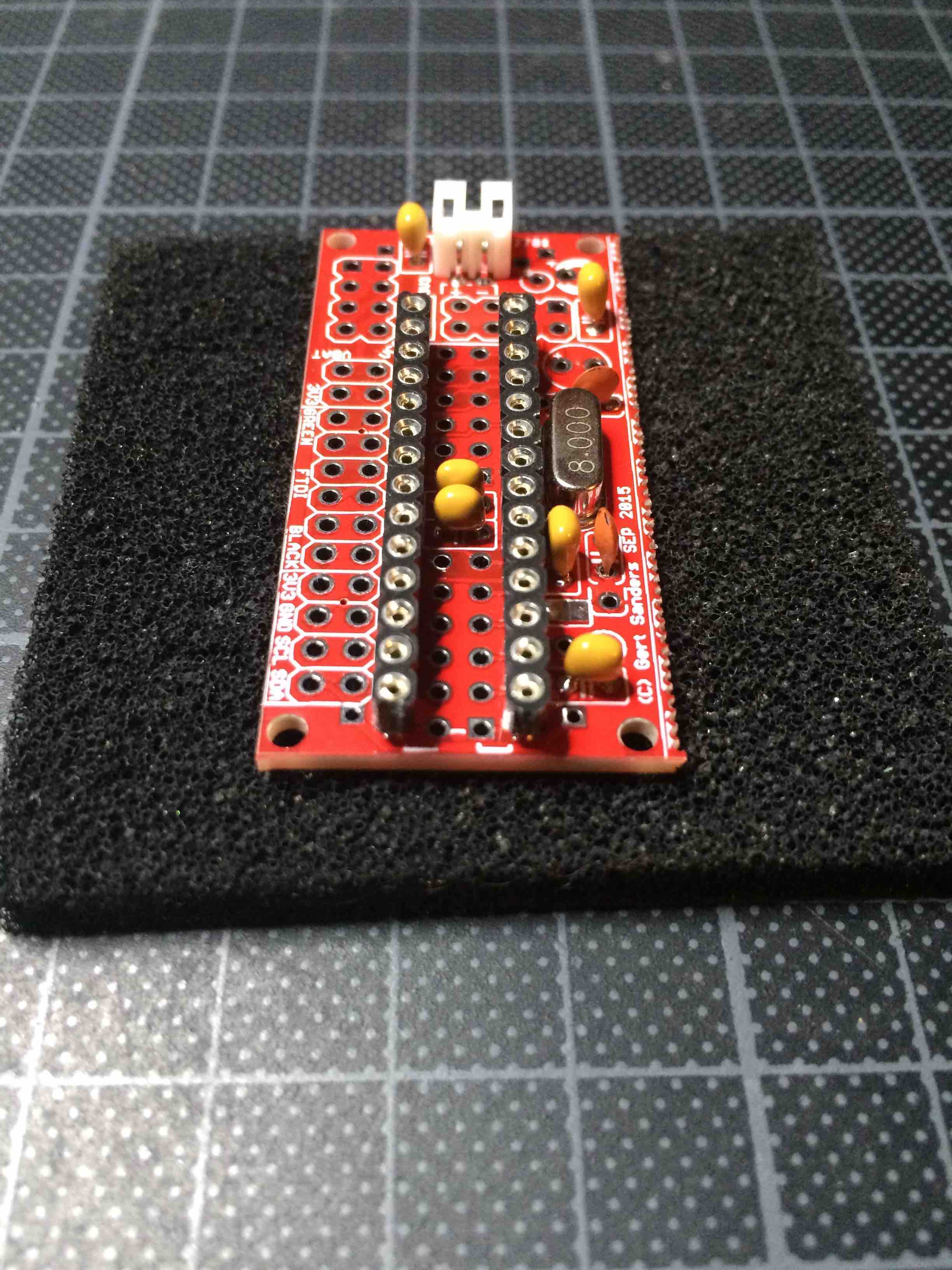
C2 decouples AVCC (the analog power input), just as C1 decouples the VCC (digital) power input. C3 stabilises the analog reference input. If you do not use the analog->digital conversion, you could skip C3 as well.I also do not use standard 28 pin sockets, but strip sockets just like BartE.
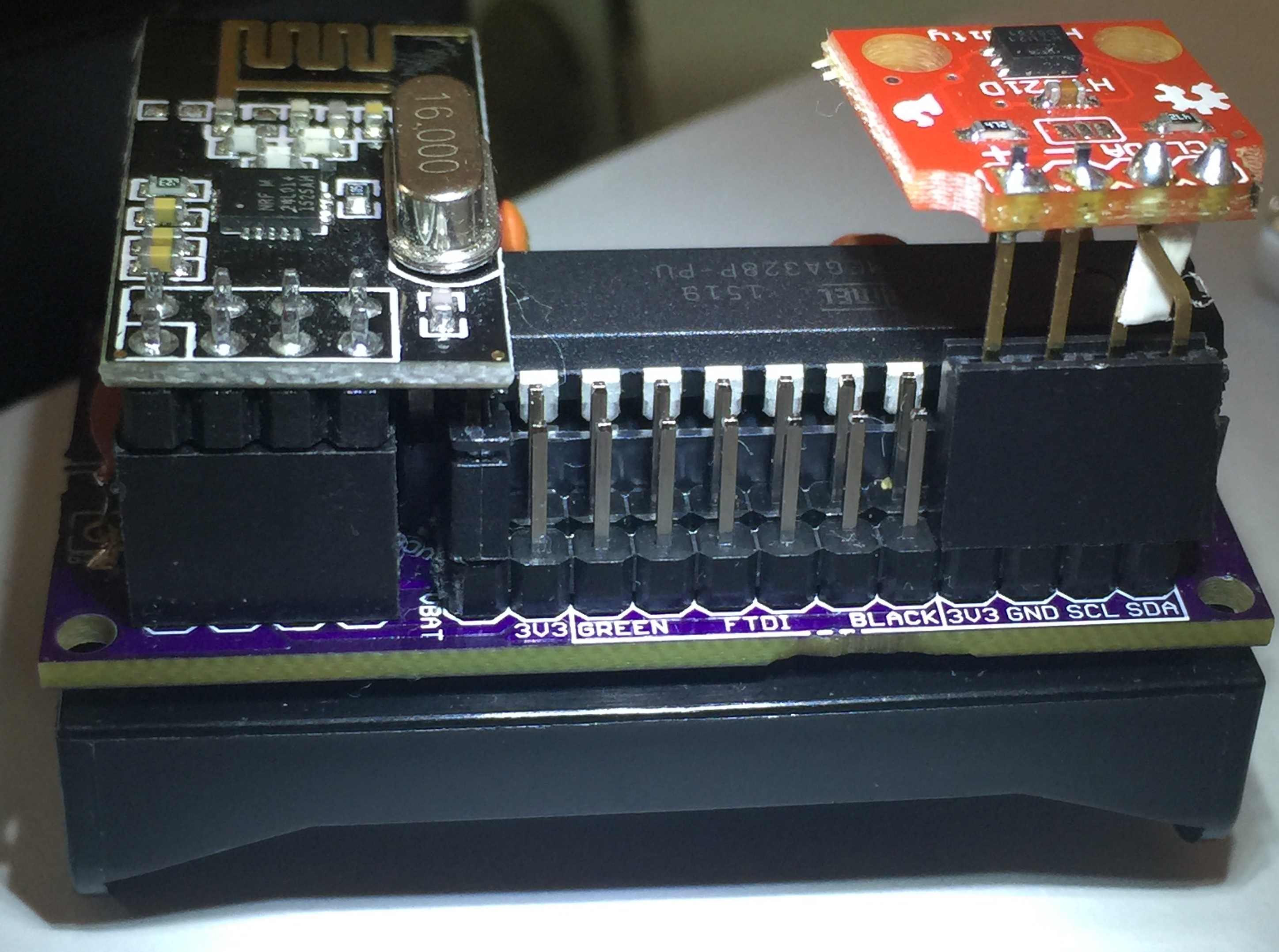
In the image here I used a standard socket, but cut away the middle "bridge" to allow mounting the decoupling capacitors.https://www.openhardware.io/uploads/568faa0cbaba42246aa57103/image/IMG_7527.jpg
In the image below I use the strips BartE mentioned:
https://www.openhardware.io/uploads/568faa0cbaba42246aa57103/image/IMG_7686.jpg
More images and details are here:
https://www.openhardware.io/view/5/Battery-based-atmega328p-sensor-no-SMD
-
I am pulling out what hair i have left.
All i am getting is this:-
find parent
send: 253-253-255-255 s=255,c=3,t=7,pt=0,l=0,sg=0,st=bc:
find parent
send: 253-253-255-255 s=255,c=3,t=7,pt=0,l=0,sg=0,st=bc:
find parent
send: 253-253-255-255 s=255,c=3,t=7,pt=0,l=0,sg=0,st=bc:
find parent
send: 253-253-255-255 s=255,c=3,t=7,pt=0,l=0,sg=0,st=bc:
find parent
send: 253-253-255-255 s=255,c=3,t=7,pt=0,l=0,sg=0,st=bc:
find parent
send: 253-253-255-255 s=255,c=3,t=7,pt=0,l=0,sg=0,st=bc:
Init complete, id=253, parent=255, distance=255
Battery:3.161 Batt%:90 Temperature:21.73C Humidity:56%
find parent
send: 253-253-255-255 s=255,c=3,t=7,pt=0,l=0,sg=0,st=bc: -
Node 253 tries to connect and fint its way to the gateway (find parent) but doesnt get any respons.
Do you have a working gateway - what does the gateway log looks like? -
Which controller are you using?
-
@GertSanders
I have been struggling to upload photos in the openhardware section of your node and I think it is better if we move our discussion here. Take a look at these: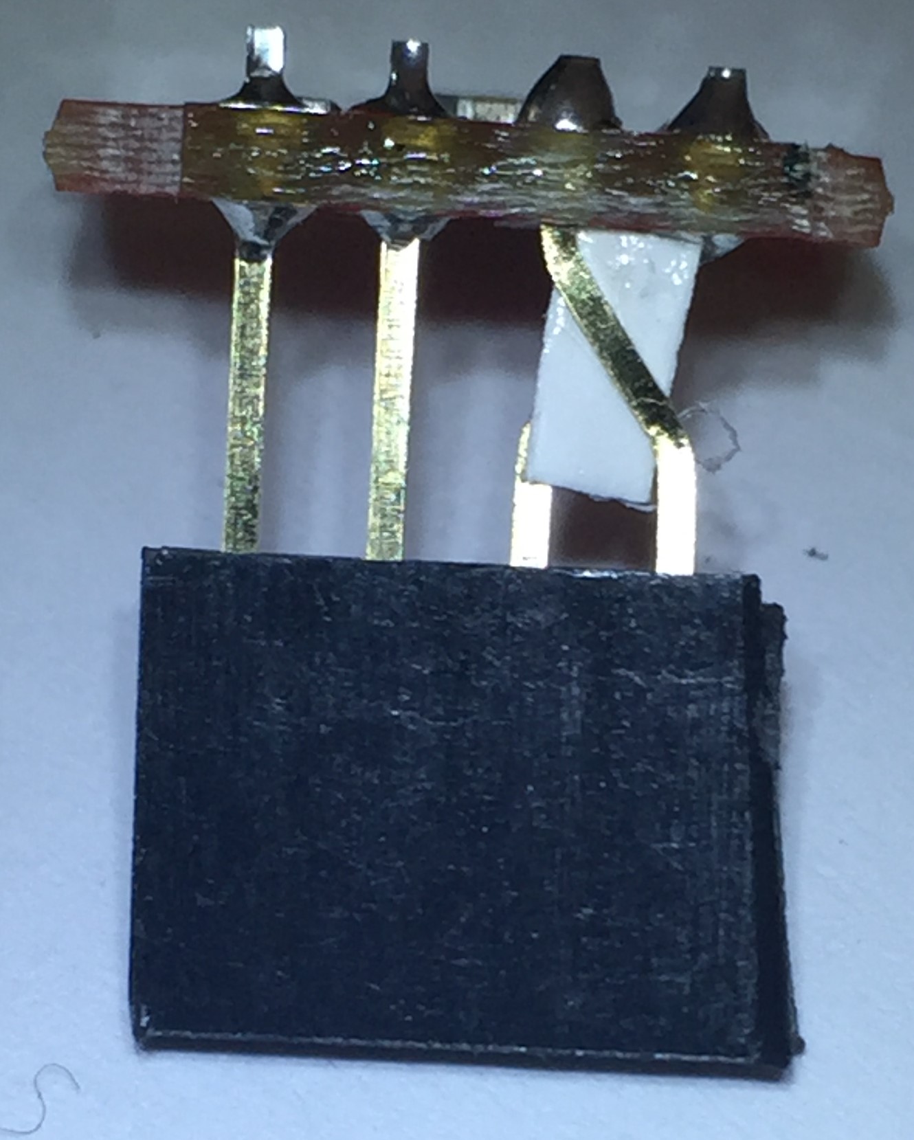
This is my answer to the problem, but I think we can have a neater solution by having jumpers deciding on SDA/SDL pin out ?
-
@GertSanders
I have been struggling to upload photos in the openhardware section of your node and I think it is better if we move our discussion here. Take a look at these:This is my answer to the problem, but I think we can have a neater solution by having jumpers deciding on SDA/SDL pin out ?
@alexsh1 There is indeed a better solution, the next version of this board will allow swapping the I2C data and clock pins :-)
-
@alexsh1 There is indeed a better solution, the next version of this board will allow swapping the I2C data and clock pins :-)
@GertSanders
Other than that I have not been using the JST connector - this may save some space unless you want to leave it as a power backup. I never used the second row pins (behind the FTDI connection) and some of them are not accessible if using a sensor connected via I2C.
Hello! It looks like you're interested in this conversation, but you don't have an account yet.
Getting fed up of having to scroll through the same posts each visit? When you register for an account, you'll always come back to exactly where you were before, and choose to be notified of new replies (either via email, or push notification). You'll also be able to save bookmarks and upvote posts to show your appreciation to other community members.
With your input, this post could be even better 💗
Register Login