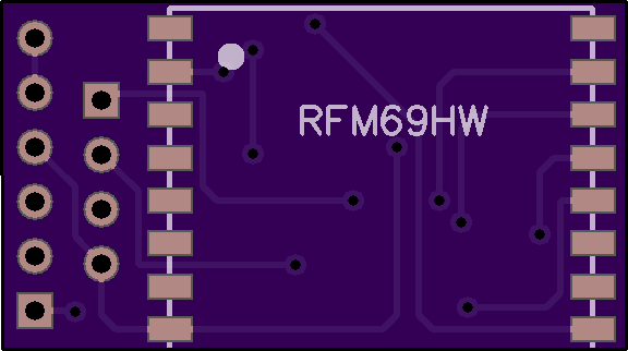
RFM69HW temp-humidity node
-
For those who can handle soldering an SMD atmega328p, the PCB can be reduced in size to less than 1 square inch in area. The usual recommendation is to use a reflow oven, though I've managed t do one by hand. I wouldn't call it easy though. Hence, the motivation for this more easily soldered design.
If you're more interested in using an NRF24L01+, then there already exist boards on this forum that are optimized for thatradio module (e.g. Gert Sander's has a number of them).
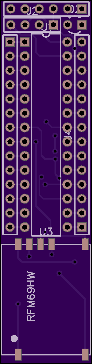
As you can see here, the smaller version--which is less easily soldered--is barely much larger than the RFM69HW module:
If powered by 2x AA batteries, though, the small size is overkill.
-
For slightly easier assembly I made it a thru-hole LED and sent it off to the FAB last night. I'll clean up the silk screen on the next iteration if this first attempt proves out.
-
Yesssss! A RFM "slim node". Way better than using an adapter board for the radio. Will you be sharing the designs for both the TH and SMD versions?
Sure, if there's interest. The one caveat is that they are Diptrace files, not the more common Eagle files. Why? I found a brief tutorial on Diptrace here: https://www.youtube.com/playlist?list=PLWy-YwxbAu8EkNv6iMsfLeH6Yahcwejwx
and that was sufficient for me to learn enough of Diptrace to actually use it. I've never done anything like this before, so that tells you how easy it is. It's liberating to quickly bang out your own PCB's, that's for sure. -
I'm also having fabbed a little FTDI adapter board:
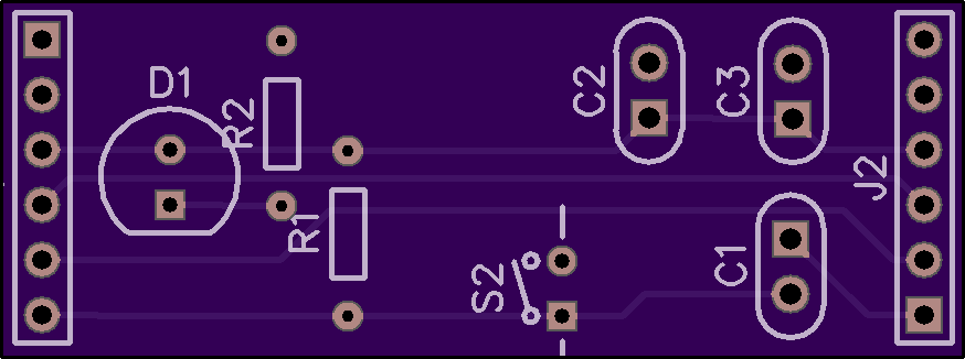
That's because a lot of the parts that you find on a mote, such as a power indicator LED, power and RF noise filtering capacitors, and pullup capacitor on the reset line needed for DTR, are common among nodes, and so repeating them on each node just to have them there for those occasions when you are FTDI connected to a PC seems redundant. This way you need just one adapter, and each node can be more simple. If you have more than one node (and who doesn't?), that translates into less parts and assembly time overall.So, you simply plug your FTDI connector on the left when you want to upload code or monitor your serial debug, and then connect your mote in on the right. The Rx and Tx lines are just passthroughs, and I did a copper ground pour on the back because it seemed fitting. I spread the parts on this board out a bit so that there'd be space for a finger to fit to hit the reset button. I was just eyeballing it, so you could probably pack them more closely if you wanted to, or even make a fully integrated FTDI board that has all this built into it. I was just aiming to make it as simple as possible without spending much time on it.
-
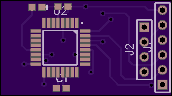
I also just now designed this pro mini interstitial board and sent it off to be fabbed:
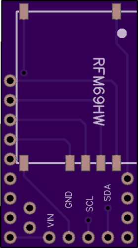
Just attach an RFM69HW and the si7021 to the board, and then plug it into a pro mini. Voila! You now have a temp-RH node. You will have to remove the LED from pin 13 on the pro mini, but that's no big deal. Also, it's obviously intended for a 3.3V pro mini, not a 5V pro mini.I suspect that for most people, this would be the simplest to put together. The board is less than 1 square inch in area.
-
BTW, you can now buy RFM69HW modules on ebay at just $2.70 each. I purchased 10x from Alice, and they arrived today. I wish LoRa modules were that cheap....
-
BTW, you can now buy RFM69HW modules on ebay at just $2.70 each. I purchased 10x from Alice, and they arrived today. I wish LoRa modules were that cheap....
I received a tiny test board today from the fab so I could see how well an smd atmega328p fits on the pads:
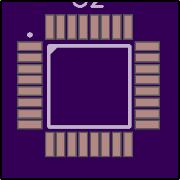
The alignment is right, but I think I can probably narrow them slightly. Is there a rule of thumb for how thin to make them, or conversely, how much spacing to put between them? My only concern is that without enough spacing between them (and I don't have any idea how much spacing is enough), there might be a risk of solder bridging. The more space, the lower the odds of that.
-
I received a tiny test board today from the fab so I could see how well an smd atmega328p fits on the pads:
The alignment is right, but I think I can probably narrow them slightly. Is there a rule of thumb for how thin to make them, or conversely, how much spacing to put between them? My only concern is that without enough spacing between them (and I don't have any idea how much spacing is enough), there might be a risk of solder bridging. The more space, the lower the odds of that.
Check the datasheet for the atmega328p-au. It has a section on PCB layout.
I would go for same width as the actual pins, and make the pads long enough to have space for some solder (when doing it by hand).
On my stamp size node I also used the smd version and that layout was not difficult to solder when using a fine tip.
-
Check the datasheet for the atmega328p-au. It has a section on PCB layout.
I would go for same width as the actual pins, and make the pads long enough to have space for some solder (when doing it by hand).
On my stamp size node I also used the smd version and that layout was not difficult to solder when using a fine tip.
@GertSanders said:
Check the datasheet for the atmega328p-au. It has a section on PCB layout.
Thanks! I'll give that a look. On my first attempt I just used the default pad layout in the diptrace library for an atmega168 (as it didn't explicitly have one for an atmega328), so I should probably verify that the dimensions are correct.
I would go for same width as the actual pins, and make the pads long enough to have space for some solder (when doing it by hand).
There might even be a case for making them a little extra long, if the board real estate allows. I believe there's a solder technique where you add solder to the pads in advance, and if they're extra long you can kinda push it onto the pins after melting it, provided you've also layered a lot of fresh flux everthing, including the pins.
On my stamp size node I also used the smd version and that layout was not difficult to solder when using a fine tip.
What kind and size of solder tip do you use?
-
@GertSanders said:
Check the datasheet for the atmega328p-au. It has a section on PCB layout.
Thanks! I'll give that a look. On my first attempt I just used the default pad layout in the diptrace library for an atmega168 (as it didn't explicitly have one for an atmega328), so I should probably verify that the dimensions are correct.
I would go for same width as the actual pins, and make the pads long enough to have space for some solder (when doing it by hand).
There might even be a case for making them a little extra long, if the board real estate allows. I believe there's a solder technique where you add solder to the pads in advance, and if they're extra long you can kinda push it onto the pins after melting it, provided you've also layered a lot of fresh flux everthing, including the pins.
On my stamp size node I also used the smd version and that layout was not difficult to solder when using a fine tip.
What kind and size of solder tip do you use?
@NeverDie
0.8 mm solder by STANNOL (HS10), packs of 100gr
The tip is around 0.8mm wide (narrowest tip I could get for my Weller station, I have an old EC2002) -
Thanks, I just ordered Hakko 0.2mm (curved) and 0.5mm (straight conical) tips from amazon. Both got good reviews. Hopefully one of them is a good match for the task, but if not, it's good to know that 0.8mm will do the business.
-
I received the board from post #1 in the mail today. I'm planning to mount the atmega328p DIP chip using machine pin female headers. It certainly can do that, but I'm thinking that on the next iteratioin it might be preferable to have the entire machine pin--not just the thinner leader part--go through the PCB, because then the plastic part of the header can be flush with the PCB (as would be the case if more typical female headers were used). Anyone tried doing that? Any reason not to do that?
-
So, to clarify, what I mean by a female machine pin header (also known as a Swiss machine pin header) is this:

Unfortunately, the only dimensioning I've been able to find is this:

which lacks the dimension I want to know, which is diameter of the larger pin body that's just above the 0.51mm diameter part of the leader pin that's meant to be pushed through the through-hole.Purely eyeballing it, it looks like it's maybe, what, twice as wide? Anyone happen to know what that dimension is?
-
I've one of these at home. I could take a measurement, but maybe someone has a better idea. ☺
-
1.35 Millimeters!
-
@TimO
Thanks! That exactly matches what my micrometer says also, so I'll go with that.So now the question is: what diameter hole should I have drilled for that? Is there a rule of thumb? e.g. Would 1.45 be too snug? Too loose?
To keep things rolling I just sent in to be fabricated a test board with 1.45mm holes . It cost just 30 cents. If anyone has an idea for a better diameter to try, let me know and I'll send in one of those as well.

-
I assembled the FTDI adapter board yesterday. I should have spaced the pads further apart on the switch (well, at least for the switch I'm using) and also on the through-hole resistors. Anyhow, I only need one, so I don't think I'll be updating it.
-
I assembled the first node from post #1 today, but it didn't work. Upon investigation, I found that one of the required traces was not there! I had generated the trace layout using diptraces auto-router, and it didn't indicate a failure. Most likely I over-constrained the problem by making the PCB board size smaller than I should have. However, if I had known that the auto-routing had failed, I could have relaxed that enough for it to succeed.
Hello! It looks like you're interested in this conversation, but you don't have an account yet.
Getting fed up of having to scroll through the same posts each visit? When you register for an account, you'll always come back to exactly where you were before, and choose to be notified of new replies (either via email, or push notification). You'll also be able to save bookmarks and upvote posts to show your appreciation to other community members.
With your input, this post could be even better 💗
Register Login