RFM69HW temp-humidity node
-
BTW, you can now buy RFM69HW modules on ebay at just $2.70 each. I purchased 10x from Alice, and they arrived today. I wish LoRa modules were that cheap....
-
BTW, you can now buy RFM69HW modules on ebay at just $2.70 each. I purchased 10x from Alice, and they arrived today. I wish LoRa modules were that cheap....
I received a tiny test board today from the fab so I could see how well an smd atmega328p fits on the pads:
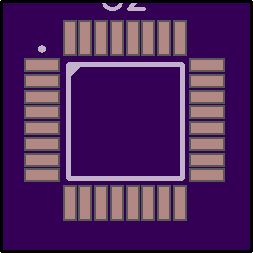
The alignment is right, but I think I can probably narrow them slightly. Is there a rule of thumb for how thin to make them, or conversely, how much spacing to put between them? My only concern is that without enough spacing between them (and I don't have any idea how much spacing is enough), there might be a risk of solder bridging. The more space, the lower the odds of that.
-
I received a tiny test board today from the fab so I could see how well an smd atmega328p fits on the pads:
The alignment is right, but I think I can probably narrow them slightly. Is there a rule of thumb for how thin to make them, or conversely, how much spacing to put between them? My only concern is that without enough spacing between them (and I don't have any idea how much spacing is enough), there might be a risk of solder bridging. The more space, the lower the odds of that.
Check the datasheet for the atmega328p-au. It has a section on PCB layout.
I would go for same width as the actual pins, and make the pads long enough to have space for some solder (when doing it by hand).
On my stamp size node I also used the smd version and that layout was not difficult to solder when using a fine tip.
-
Check the datasheet for the atmega328p-au. It has a section on PCB layout.
I would go for same width as the actual pins, and make the pads long enough to have space for some solder (when doing it by hand).
On my stamp size node I also used the smd version and that layout was not difficult to solder when using a fine tip.
@GertSanders said:
Check the datasheet for the atmega328p-au. It has a section on PCB layout.
Thanks! I'll give that a look. On my first attempt I just used the default pad layout in the diptrace library for an atmega168 (as it didn't explicitly have one for an atmega328), so I should probably verify that the dimensions are correct.
I would go for same width as the actual pins, and make the pads long enough to have space for some solder (when doing it by hand).
There might even be a case for making them a little extra long, if the board real estate allows. I believe there's a solder technique where you add solder to the pads in advance, and if they're extra long you can kinda push it onto the pins after melting it, provided you've also layered a lot of fresh flux everthing, including the pins.
On my stamp size node I also used the smd version and that layout was not difficult to solder when using a fine tip.
What kind and size of solder tip do you use?
-
@GertSanders said:
Check the datasheet for the atmega328p-au. It has a section on PCB layout.
Thanks! I'll give that a look. On my first attempt I just used the default pad layout in the diptrace library for an atmega168 (as it didn't explicitly have one for an atmega328), so I should probably verify that the dimensions are correct.
I would go for same width as the actual pins, and make the pads long enough to have space for some solder (when doing it by hand).
There might even be a case for making them a little extra long, if the board real estate allows. I believe there's a solder technique where you add solder to the pads in advance, and if they're extra long you can kinda push it onto the pins after melting it, provided you've also layered a lot of fresh flux everthing, including the pins.
On my stamp size node I also used the smd version and that layout was not difficult to solder when using a fine tip.
What kind and size of solder tip do you use?
@NeverDie
0.8 mm solder by STANNOL (HS10), packs of 100gr
The tip is around 0.8mm wide (narrowest tip I could get for my Weller station, I have an old EC2002) -
Thanks, I just ordered Hakko 0.2mm (curved) and 0.5mm (straight conical) tips from amazon. Both got good reviews. Hopefully one of them is a good match for the task, but if not, it's good to know that 0.8mm will do the business.
-
I received the board from post #1 in the mail today. I'm planning to mount the atmega328p DIP chip using machine pin female headers. It certainly can do that, but I'm thinking that on the next iteratioin it might be preferable to have the entire machine pin--not just the thinner leader part--go through the PCB, because then the plastic part of the header can be flush with the PCB (as would be the case if more typical female headers were used). Anyone tried doing that? Any reason not to do that?
-
So, to clarify, what I mean by a female machine pin header (also known as a Swiss machine pin header) is this:

Unfortunately, the only dimensioning I've been able to find is this:

which lacks the dimension I want to know, which is diameter of the larger pin body that's just above the 0.51mm diameter part of the leader pin that's meant to be pushed through the through-hole.Purely eyeballing it, it looks like it's maybe, what, twice as wide? Anyone happen to know what that dimension is?
-
I've one of these at home. I could take a measurement, but maybe someone has a better idea. ☺
-
1.35 Millimeters!
-
@TimO
Thanks! That exactly matches what my micrometer says also, so I'll go with that.So now the question is: what diameter hole should I have drilled for that? Is there a rule of thumb? e.g. Would 1.45 be too snug? Too loose?
To keep things rolling I just sent in to be fabricated a test board with 1.45mm holes . It cost just 30 cents. If anyone has an idea for a better diameter to try, let me know and I'll send in one of those as well.

-
I assembled the FTDI adapter board yesterday. I should have spaced the pads further apart on the switch (well, at least for the switch I'm using) and also on the through-hole resistors. Anyhow, I only need one, so I don't think I'll be updating it.
-
I assembled the first node from post #1 today, but it didn't work. Upon investigation, I found that one of the required traces was not there! I had generated the trace layout using diptraces auto-router, and it didn't indicate a failure. Most likely I over-constrained the problem by making the PCB board size smaller than I should have. However, if I had known that the auto-routing had failed, I could have relaxed that enough for it to succeed.
-
So, I was able to make the board work by soldering on a single "oops" wire to compensate for the missing trace. I guess I'll be redoing this board so that's not required on future builds. The FTDI adapter board also had an oops that I fixed without much difficulty. Using the adapter board I've verified I can upload new sketches to the node from post #1. The reset button also works as intended. So, the adapter board feasibility is now proven.
-
I took a shot at soldering the smaller board with the much tinier atmega328p, but for now I've concluded that hand soldering such a small chip is simply more work than it's worth. Perhaps with a reflow oven....
I'm still waiting for the interstitial board to arrive.
-
Soldering an atmega328 smt is easy:
https://www.youtube.com/watch?v=UeCZ9AMG3Vo
according to that guy, anyway. Maybe the longer pads makes it so? -
I took a shot at soldering the smaller board with the much tinier atmega328p, but for now I've concluded that hand soldering such a small chip is simply more work than it's worth. Perhaps with a reflow oven....
I'm still waiting for the interstitial board to arrive.
This has a lot of detail about soldering the atmega328 surface mount:
https://www.youtube.com/watch?v=-yc3zEe0RA0
So, though it's obviously doable, I still wouldn't say it's "easy." -
This has a lot of detail about soldering the atmega328 surface mount:
https://www.youtube.com/watch?v=-yc3zEe0RA0
So, though it's obviously doable, I still wouldn't say it's "easy."I finally had success using the Dave Jones tack and reflow method. The hardest part is just ensuring that the chip is properly aligned after the tack. From that point on, iit goes relatively easy.
-
So, LED is blinking like it should, and I can download sketches to it. I plugged in an si7021 board, and that's working too:
Humidity: 44.42 Temperature: 22.22
Humidity: 44.40 Temperature: 22.22
Humidity: 44.43 Temperature: 22.23
Humidity: 44.42 Temperature: 22.22
Humidity: 44.43 Temperature: 22.21
Humidity: 44.43 Temperature: 22.22
Humidity: 44.44 Temperature: 22.22Looks as though a BME280 board, which has the same pinout as the si7021 board, should work also.

I tried the adafruit library on such a BME280, but it says it can't find the sensor. So, I tried the sparkfun library instead, and it is outputing false information:Temperature: 0.00 degrees C
Temperature: 32.00 degrees F
Pressure: 0.00 Pa
Altitude: 45846.20m
Altitude: 150414.04ft
%RH: 0.00 %Looking at the back of the BME280 board , it looks like it may have a voltage regulator and/or level converter on it (?)..

Since I'm feeding it 3.3v, not 5v, then perhaps that's the problem.The part is 662K, and sure enough, it's a voltage regulator:
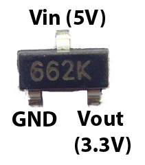
If I remove that and short Vin to the 3v3 lead, maybe it will work....
So, to see if it works at all, I hooked up the BME280 board to an arduino uno at 5v, and... still no joy. Apparently, I received a defective BME280. :disappointed: Murphy's Law strikes again. Therefore, I'll exchange it for another one. Meanwhile, I'll use the si7021.
Hello! It looks like you're interested in this conversation, but you don't have an account yet.
Getting fed up of having to scroll through the same posts each visit? When you register for an account, you'll always come back to exactly where you were before, and choose to be notified of new replies (either via email, or push notification). You'll also be able to save bookmarks and upvote posts to show your appreciation to other community members.
With your input, this post could be even better 💗
Register Login