-
Ok I have finally figured it out. You need to open the "PCBNew" pcb designer part of KiCad -> "Einstellungen" (Settings) -> "Footprint Bibliothekswizard" (Library Wizard) -> Github Repo... (insert https://github.com/mysensors-kicad). That makes them available in the PCB editor.
For the Eeschema editor you need to go to "Einstellungen" (Settings) -> "Baubiliotheksdateien" (Partslibrary) and add a custom path to your cloned git repo. Then you can "Hinzufügen" (add) them in the list above and use them in your project.
Perhaps this helps someone in the future. Not the most intuitive part of the program yet^^@LastSamurai said:
Ok I have finally figured it out. You need to open the "PCBNew" pcb designer part of KiCad -> "Einstellungen" (Settings) -> "Footprint Bibliothekswizard" (Library Wizard) -> Github Repo... (insert https://github.com/mysensors-kicad). That makes them available in the PCB editor.
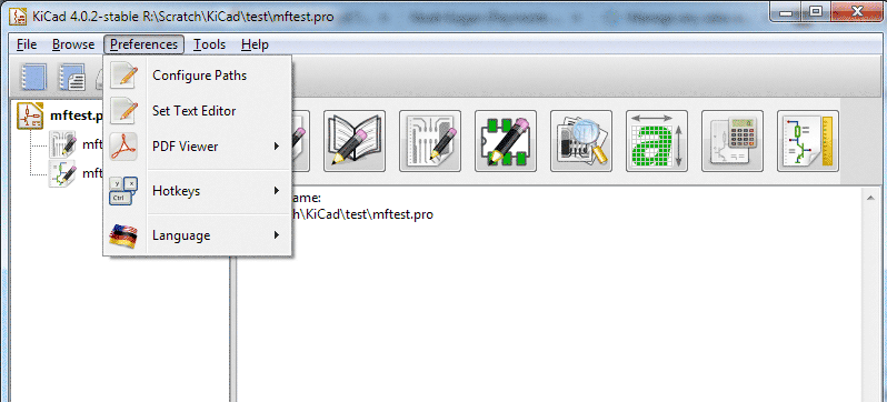
Could anyone explain how I do the first step (open the "PCBNew" pcb designer part of KiCad)?
I have started Kicad but can't see "Library Wizard" under the "Preferences" menu so I think I'm lost.
-
@mfalkvidd you have to open pcbnew pcb designer first. That's the third icon in the row on the right side of your screenshot.
thanks @Anduril !
I got it working now.
If anyone gets the following error:
Errors were encountered loading footprints
IO_ERROR: footprint library path 'R:\eclipse-workspace\mysensors-kicad/mysensors_connectors.pretty' does not exist
from C:/Jenkins/workspace/windows-kicad-msys2-stable/src/kicad-4.0.2/pcbnew/kicad_plugin.cpp : FootprintEnumerate() : line 1758
You just need to flip the / to \ (since Windows uses \)
My fp-lib-table now looks like this at the end:
(lib (name mysensors_arduino)(type Github)(uri https://github.com/mysensors-kicad/mysensors_arduino.pretty)(options "allow_pretty_writing_to_this_dir=${MYSLOCAL}\mysensors_arduino.pretty")(descr "")) (lib (name mysensors_buttons)(type Github)(uri https://github.com/mysensors-kicad/mysensors_buttons.pretty)(options "allow_pretty_writing_to_this_dir=${MYSLOCAL}\mysensors_buttons.pretty")(descr "")) (lib (name mysensors_connectors)(type Github)(uri https://github.com/mysensors-kicad/mysensors_connectors.pretty)(options "allow_pretty_writing_to_this_dir=${MYSLOCAL}\mysensors_connectors.pretty")(descr "")) (lib (name mysensors_handsoldering)(type Github)(uri https://github.com/mysensors-kicad/mysensors_handsoldering.pretty)(options "allow_pretty_writing_to_this_dir=${MYSLOCAL}\mysensors_handsoldering.pretty")(descr "")) (lib (name mysensors_leds)(type Github)(uri https://github.com/mysensors-kicad/mysensors_leds.pretty)(options "allow_pretty_writing_to_this_dir=${MYSLOCAL}\mysensors_leds.pretty")(descr "")) (lib (name mysensors_network)(type Github)(uri https://github.com/mysensors-kicad/mysensors_network.pretty)(options "allow_pretty_writing_to_this_dir=${MYSLOCAL}\mysensors_network.pretty")(descr "")) (lib (name mysensors_obscurities)(type Github)(uri https://github.com/mysensors-kicad/mysensors_obscurities.pretty)(options "allow_pretty_writing_to_this_dir=${MYSLOCAL}\mysensors_obscurities.pretty")(descr "")) (lib (name mysensors_radios)(type Github)(uri https://github.com/mysensors-kicad/mysensors_radios.pretty)(options "allow_pretty_writing_to_this_dir=${MYSLOCAL}\mysensors_radios.pretty")(descr "")) -
Sorry for hijacking this old thread, but I have problems finding libraries for all common parts. Does anybody have a working library for the HlK-PM01 power supply? There are tons of libs for the pcb layout, but i cannot find any symbols. How do you guys find this stuff? I am just asking google for "KiCad HlK-PM01". :D
-
Usually I end up making a symbol myself, or use something that resembles the component that I want to add to the pcb
So basicly I could use any power supply in the circuit and still HLK-PM01 in the layout? How do I map this?
-
You map schematic symbols to pcb symbols using CvPcb. in your schematic, it's the 3rd icon from right, in the toolbar above your editor window
The work process is normally as follows:
- Create your schematics
- Generate netlist
- Assign foot prints to the components, using CvPcb
- Re-generate netlist, as it now will contain info about footprints.
- Load netlist in pcbNew
- Do your layout in pcbNew
-
Thx, this should get me started. I've never successfully designed a pcb before. I had a look at Eagle a few month ago and gave up. I hove I'll have more success with KiCad. Your help is very welcome. :)
@Jan-Gatzke I haven't gotten as far as you (i.e. I haven't gotten started wih pcb design yet) but I have collected a few guides that I think will help me to get going. Maybe they are useful for you as well:
-
@Jan-Gatzke I haven't gotten as far as you (i.e. I haven't gotten started wih pcb design yet) but I have collected a few guides that I think will help me to get going. Maybe they are useful for you as well:
Thx, this definitly saves some Google time. ;)