Powering mote 24/7 using only a supercap and solar


  • Hero Member

    @scalz
    Out of curiosity, why did you choose such a large inductor? I notice that the "stripped" BQ25504 pcb (photo above) did the same thing. Are there advantages to the larger size?


  • Hero Member

    @NeverDie said:

    @scalz
    Out of curiosity, why did you choose such a large inductor? I notice that the "stripped" BQ25504 pcb (photo above) did the same thing. Are there advantages to the larger size?

    Nevermind. I see now from your schematic that you're using the coilcraft inductor from Table 1 of the DS.


  • Hero Member

    Interestingly, looking at the Tindie board now, it's clear based on its inductor's dimensions that the Tindie board is not using one of the Table 1 recommended inductors. Perhaps that explains why the Tindie board appears to be sucking wind at the lower voltages.


  • Hero Member

    @NeverDie
    Coilcraft doesn't seem very available in the US, but Wurth has a similar one that's still on the DS table list that's probably a good substitute: http://www.digikey.com/product-detail/en/wurth-electronics-inc/744031220/732-1012-1-ND/1639073

    Also, I'll have to update my board to use a larger inductor. I had blithely assumed, based on the Tindie board, that an 0805 would be sufficient, but now that I'm digging into it probably not.


  • Hero Member

    @NeverDie
    I take it back. The Wurth component I just referenced has a rather complex looking land pattern.

    Fortunately, the last remaining component on the Table 1 recommended list is a Wurth that has a much easier land pattern: http://www.digikey.com/product-detail/en/wurth-electronics-inc/744025220/732-2619-1-ND/2445718


  • Hardware Contributor

    @NeverDie
    yep from guidelines.
    but also because it's better to use shielded inductors for multiple reasons like EMI..and also good inductors and parts give better perf, efficiency etc.. lot of docs on this.

    That said, the footprint i use is also compatible with the 0805 advised in datasheet if i remember. it's possible to use both ref for the same footprint i've not the datasheet in front of me right now but width shoud be ok.


  • Hero Member

    It seems as though TI's evaluation board ignores the design recommendations given in the datasheet, in particular: "...it is highly recommended that no ground planes be poured near the voltage setting resistors or the sample and hold capacitor." In the case of the TI's evaluation board, virtually the entire bottom layer is a ground plane. I don't know what to make of that.

    Anyhow, I ordered the Wurth inductors. I also ordered a 3x3 QFN-16 solder stencil as some fallback insurance, as the BQ25504 looks like it will be very challenging to solder.


  • Hero Member

    Also, the layout guidelines say, " It is best to use vias and bottom traces for connecting the inductor to its respective pins instead of the capacitors." Yet, the recommended layout doesn't do that.


  • Hero Member

    Part of what's strange is the Recommended Layout (Figure 34 in the datasheet) shows pin 12 belonging to a different ground plane than pin 13. Yet, the schematic shows pins 12 and 13 wired directly together.

    @scalz
    Just where are the two different ground planes supposed to connect together? Or is one supposed to float relative to the other?


  • Hardware Contributor

    @NeverDie
    ok i'll put on my git&openhardware asap.

    about the planes, you're right. I've a little doubt. on most designs, it's directly to gnd. i understand about the layout guidelines. but the datasheet picture layout is a bit confusing, if it's internally connected or not..i'll check a bit later.

    good point 😉


  • Hero Member

    @scalz

    Section 11.1 says, "When laying out the non-power ground return paths (e.g. from resistors and CREF), it is recommended to use short traces as well, separated from the power ground traces and connected to AVSS pin 12. This avoids ground shift problems, which can occur due to superimposition of power ground current and control ground current. The PowerPad should not be used as a power ground return path."

    I think that's why in the Recommended Layout (Figure 34), pins 12 and 13 are not connected directly together. However, on your board, they are directly connected, probably because of the schematic.

    What do they mean by "The PowerPad"? Do they mean the thermal pad beneath the chip? Maybe that's another reason why pin 12 is not connected to the thermal pad in the Recommended Layout.

    I don't know what the right answer is. I'm just trying to make sense of what seem like inconsistencies in the datasheet.


  • Hero Member

    I suppose if worse came to worst, we could try answering the question empirically by using a test setup similar to this:

    0_1480288951886_BQ25504_v14_top.png
    0_1480288994462_BQ25504_v14_bottom.png

    In this instance I partitioned the data ground from the power ground, and the two are not connected. However, via the header pins, a jumper could be connected between the two grounds. The experiment would be to try it both ways--connected vs. unconnected--and see which performs better.


  • Hero Member

    The through holes on the stripped BQ25504 PCB (above)from Osh Park have too small a diameter to fit header pins into. In fact, it would require a very narrow gauge wire (narrower than what I have) to fit into it. So, unfortunately, I have doubts as to whether I will be able to test it, let alone use it.

    This is all rather disappointing. 😖 So far nothing about the BQ25504 has been easy.


  • Hero Member

    Not that it proves anything, but using KiCAD to look at the BQstripped PCB, I notice that the PCB designer chose to connect pins 12 and 13 both directly to each other and directly to the thermal pad.


  • Admin

    @NeverDie said:

    Not that it proves anything, but using KiCAD to look at the BQstripped PCB, I notice that the PCB designer chose to connect pins 12 and 13 both directly to each other and directly to the thermal pad.

    Did you say KiCAD? 👍 👍 👍


  • Hero Member

    @blacey said:

    Did you say KiCAD? 👍 👍 👍

    Yup. I had to use KiCAD to confirm the proper chip orientation before attempting to hand solder it to their PCB. Looks like a nice program.

    I had doubts I could hand solder the BQ25504, but I tried it using Dave Jones's tack and reflow method, and to my untrained eye it looks like it came out OK, despite the chip not being completely well aligned with the solder pads:
    0_1480378211590_BQ25504_1.jpg

    0_1480378225784_BQ25504_2.jpg

    0_1480378245176_BQ25504_3.jpg

    0_1480378270381_BQ25504_4.jpg

    The Wurth inductors arrived today, so I'll have a go at soldering that on next. Hopefully the BQstripped PCB designer picked the same one I did!


  • Hero Member

    Looks as though the inductor hand soldered as well:
    3_1480381576419_inductor4.jpg 2_1480381576419_inductor3.jpg 1_1480381576418_inductor2.jpg 0_1480381576418_inductor1.jpg


  • Hero Member

    Interestingly, if one looks at the KiCad schematic for the bqstripped PCB, you will notice that it draws a distinction between regular GND and GNDPWR:
    0_1480428663373_kicad_schematic.pdf

    However, as already noted, that distinction seems to be cast aside when they laid out the PCB traces, since pins 12 and 13 are connected together directly by a trace. Indeed, the schematic explicitly shows GNDPWR connected to GND. So, why create the distinction in the first place?


  • Hardware Contributor

    @NeverDie
    this is for the power gnd plane regarding the analog gnd plane. analog for instance should be connected at one point. but then in practice like you said it looks a bit different...
    don't worry too much i think!
    The good in this, is i think, you have learnt good things (taking care of datasheet guidelines etc...) for future 👍


  • Hero Member

    @scalz

    I want to do it properly. I'm just not sure what is proper with this chip. What is the technically correct way to do it?

    P.S. I ordered some 30AWG wire for hooking up the BQstripped PCB.


  • Hero Member

    I had to order some 4.7uF smd 0603 capacitors and 4.42M ohm 0603 resistors.

    The DS also calls for 15.62M ohm resistors, but the closest thing that Digikey carries is 15M ohm 0603 smd's, so that's what I ordered.

    Meanwhile I did solder the 10nf capacitors to the BQstripped pcb, as I had those on hand. If I had it to do over, I would probably have soldered them prior to soldering the BQ25504 and the 22uH inductor, as those parts were in the way.


  • Hero Member

    Just a few notes on a conservative approach to component selection for boost converters that I've lately gleaned from reading various datasheets:

    1. Ideally, capacitors should be rated X5R or X7R.

    2. For inductors, generally speaking the lower the DCR the better, provided that the saturation current remains appropriately high enough. For instance, the B82462G4 series (http://www.digikey.com/product-search/en/inductors-coils-chokes/fixed-inductors/196627?k= +B82462G4&k=&pkeyword= +B82462G4&pv7=2&mnonly=0&newproducts=0&ColumnSort=0&page=1&quantity=0&ptm=0&fid=0&pageSize=500 ) has much lower DCR than any of the datasheet recommended inductors. These inductors are more expensive, but their use should, in theory, lead to higher efficiency and/or lower start/operating voltages. Also, I suspect the Tindie board's performance is impaired by its choice of inductor, because I haven't seen specs on any inductors as small as theirs is that has a low DCR.


  • Hardware Contributor

    +1 for X5R/X7R 😉


  • Hero Member

    @scalz said:

    +1 for X5R/X7R 😉

    I looked into it a little bit more, and I'm defaulting to X7R for everything, unless there's good reason not to: https://www.maximintegrated.com/en/app-notes/index.mvp/id/5527 The article also provides good reason to favor larger package sizes, up to size 1210, if the design allows.


  • Hardware Contributor

    @NeverDie
    that's also what i do, ceramic, x7r everywhere when possible. nice article, thx for sharing 😉


  • Hero Member

    I've settled on this series of shielded inductor as having a good bang for buck ratio: low DCR, high current rating, and relatively low price: http://www.digikey.com/catalog/en/partgroup/dg-series/53965?mpart=1255AY-220M=P3&vendor=490

    If anyone knows of a better series than that one, please post.


  • Hero Member

    For comparison, I ordered an inexpensive ($0.91, including shipping) 6v panel: https://www.aliexpress.com/item/6V-0-6W-Solar-Power-Panel-Module-DIY-Small-Cell-Charger-For-Light-Battery-Phone-Toy/32723002222.html?spm=2114.13010608.0.0.OYll8L

    It's a little bigger, but still reasonably small (a little more than 2"x3" in size). Mainly, though, the energy harvesting chips that work at very low voltages are surprisingly expensive, so maybe this higher voltage panel will allow the use of less expensive chips that have higher start voltages. Of course, indoors I don't expect it will ever get to a full 6v under load, but I do expect that under the same lighting conditions it will offer up higher voltages at the same load as the cheap garden solar cell referenced in the OP.


  • Hero Member

    @scalz I was just now noticing that you like to put silkscreen between component pads:
    0_1481325056200_bq25504_scalz.png

    Does silkscreen work the same as solder mask, in that it sorta "repels" molten solder away from it? I really don't know, but I've been assuming that it doesn't. In fact, I've gone out of my way to move silkscreen away from the solder pads out of fear it might contribute to inadvertent solder bridging between pads.

    Anyone know?


  • Hardware Contributor

    @NeverDie
    well, sometimes i think to not put them at all! especially when i want to make things compact..at a moment, it becomes difficult to fit them, and you can't reduce fontsize because it's ugly. usually, i use 32mils.

    I've never had short because of this though.


  • Hero Member

    @scalz said:

    @NeverDie
    well, sometimes i think to not put them at all! especially when i want to make things compact..at a moment, it becomes difficult to fit them, and you can't reduce fontsize because it's ugly. usually, i use 32mils.

    I've never had short because of this though.

    Actually, I wasn't referring so much to the letters and numbers--which are off to the side-- so much as the little dashes and lines that appear between the pads. The letters and numbers are useful.


  • Hardware Contributor

    I know, you're right, these are useful 😉
    but when doing compact stuff, it's not always easy to display everything well..
    I usually have my computer display in front of me when assembling, or i print the layout x4..so i don't look at the silkscreen so much..

    About "repels", if i understand right, i have never got short during soldering. I think you mean silkscreen, between parts, would help to bridge soldering? but no never got problem.
    I often use stencil+reflow oven, so there is only the solder needed. For proto, generally i almost assemble at hand, still no problem 🙂


  • Hero Member

    In that case, maybe it's a non-issue, which would be good to know for future reference.


  • Hero Member

    @scalz

    0_1481325056200_bq25504_scalz.png

    I see now why your board has 10 resistors instead of TI's reference schmatic's 9 resistors. It's because there doesn't seem to exist an off-the-shelf 15.62M-Ohm 0609 resistor, even though TI apparently thinks such a component does exist. I know Digikey doesn't stock any 15.62M-Ohm 0609 resistors, that's for sure. So, your two series resistors are probably a 15M-Ohm resistor and a 620K-Ohm resistor, both of which Digikey sells.


  • Hero Member

    @scalz
    I worked out the following as the mapping from resistor labels on your board to resistor values (assuming the target is Figure 14 from the DS):
    R1 = 4.42M
    R2 = 15M
    R3 = 620K
    R4 = 1.43M
    R5 = 4.22M
    R6 = 4.42M
    R7 = 4.02M
    R8 = 5.9M
    R9 = 4.42M
    R10 = 5.6M


  • Hardware Contributor

    i don't remember, i'll look at this later. but i posted the schematic some posts above if it can help.


  • Hero Member

    From the fab I've already received my board, your board, and obvioiusly the "stripped" board (photos above). On Thursday I should receive from Digikey resistors with precisely the values in the above list. I'll then be able to finish assembling the boards and see how their performance compares. TI has a paper for measuring the BQ25504 efficiency: http://www.ti.com/lit/an/slua691/slua691.pdf


  • Hero Member

    @scalz
    I assembled both your board and my board today and did a quick test. The good news is that both boards appear to function with a cold start voltage of about 330mv, and for that reason it appears that both boards outperform the Tindie board. I am guessing that is, at least in part, because they use one of the datasheets recommended inductors, as compared to the Tindie Board, which does not appear to.


  • Hero Member

    I've played with the BQ25504 boards only a little bit thus far, but the truth that the datasheet glossed over in the executive summary section is that at the very low voltages (330mv+), the efficiency is terrible up until it charges up the caps to reach a threshhold voltage of around 2 volts or so. Those ultra-low voltages are the "cold start" phase, and the aim of that is, apparently, to bootstrap itself using available energy up to the threshhold voltage (maybe there's a better term for it). So, the trick to using this chip appears to be to maintain at least the threshhold voltage on the caps. You really don't want to ever invoke the cold start mechanism, because the the cold start efficiency appears to be quite miserable. So, while it is true to say that it works at ultra low voltages, it's just a partial truth that leaves a lot unsaid.

    So, if one starts with the assumption that a relatively high voltage (say 2 volts, give or take) must be maintained on the caps in order for this to be practical, it really has me wondering now how this chip compares to other boost chips under the same assumptions. Fortunately, I have test boards for a number of different kinds of boost chips already in the pipeline. 😄


  • Hero Member

    A closer reading of the cold start section of the datasheet (Section 8.4) confirms my initial observations. VSTOR_CHGEN is what I was calling the "threshhold voltage" and is typically around 1.8v. VSTOR must be greater than VSTOR_CHGEN before cold start ends. The datasheet conceeds that cold start runs an "inefficient" boost converter. Just how inefficient? Well, I haven't seen any curves in the datasheet that answer that precisely (perhaps they were deleted by the marketing department?). Apparently, if you want to know that vital information, you have to compile your own data. I guess TI either doesn't know themselves (unlikely), or they're just not sharing.. Gee, thanks TI

    However, the reality is worse than what I initially surmised, especially if using a supercap: That's because a discharged supercap will crash VSTOR, and so the chip could remain stranded in cold-start mode. Quoting the datasheet: "When large, discharged super capacitors with high DC leakage currents are attached, the intial charge time can be signficant." Yeah, no kidding. But, it appears there's also a notion for how to workaround this problem: "It is highly recommended to add an external PFET between the system load and VSTOR. An inverted VBAT_OK signal can be used to drive the gate of this system-isolating, external PFET."

    So..... now I need to figure out the brass tacks of how to do that and probably redo the PCB to include such a PFET.


  • Hero Member

    I think I'll try using a load switch. That way I can use the BAT_OK signal directly, without having to invert it. What I don't presently know is how fast the BAT_OK signal changes. If it lags considerably, then there's a risk that VSTOR might fall back into the cold start region before the current draining from vstor into the supercap can be shut off.


  • Hero Member

    I found this curve:
    0_1481986422095_curve.png
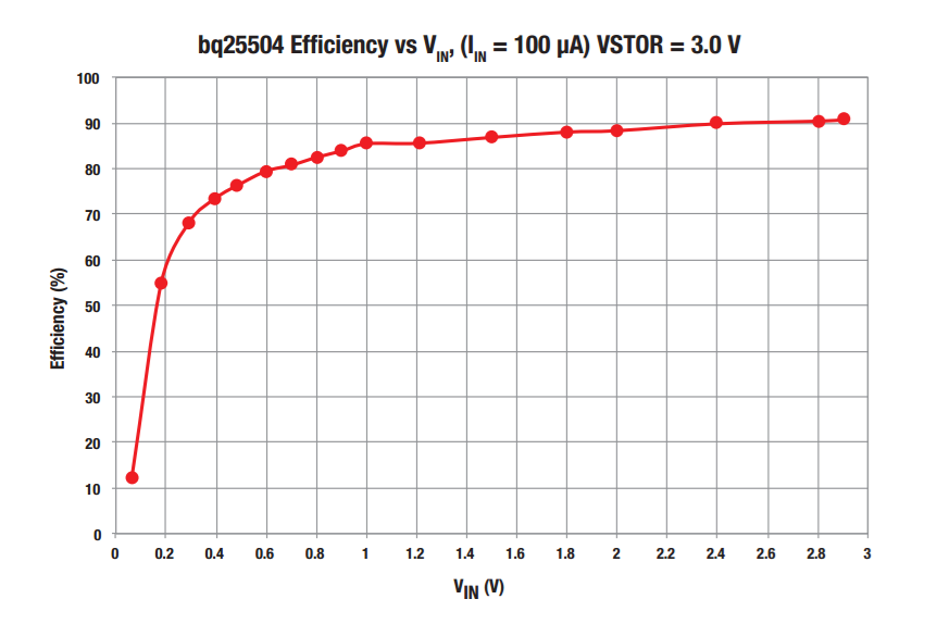
    not in the datasheet, but here: http://www.ti.com/lit/ml/slpt026a/slpt026a.pdf

    You'll note that it shows VSTOR = 3.0V, which I think is probably key to getting anything worthwhile from this chip. Anyhow, as long as VSTOR=3.0V, it's a pretty impressive curve.


  • Hero Member

    TI makes an "ultra low leakage load switch" which might be a good fit: http://www.ti.com/lit/ds/symlink/tps22860.pdf


  • Hero Member

    OK, I just put together a breakout board for the TPS22860 to audition it for this new role. I just now sent it to the fab, so it will be another two weeks (!) before I'll know. I just hate how these fab iterations stretch these projects out far too long.


  • Hero Member

    So, what should the programmed voltage cut-off's be? Here's my first pass at that:

    VBAT_UV = 0 volts. // it's a capacitor, so you can't overdischarge it.

    VBAT_OV = 3.6 volts // because we don't want to run the mote at more than 3.6 volts.

    VBAT_UV_HYST = 1.9v. // Note sure. To avoid the cold start inefficiency if the supercap is flat, it shouldn't be lower than 1.8v. If the VSTOR cap is ultra low leakage, then maybe 1.9v would keep the BQ25504 out of the cold start zone for long enough (?). If not, I might need to utilize a higher capacitance VSTOR.

    VBAT_OV_HYST = 2.0v. // Another guess. Needs to be higher than VBAT_UV_HYST, or there won't be any charge to transfer to the supercap. On the other hand, a higher voltage would lead to greater inefficiency if the supercap voltage is low.

    As long as the supercap's voltage is above VBAT_UV_HYST, then the supercap and VSTOR will remain connected.


  • Hero Member

    Translating the above programmed voltages into resistor values that can be purchased on Digikey yields the following:

    ROV1 = 5.1M
    ROV2 = 4.7M
    ROK1 = 6.2M
    ROK2 = 3.3M
    ROK3 = 510K
    RUV1 = 10M
    RUV2 = 0 or 1 ohm (doesn't matter which)


  • Hero Member

    I received the MCP1640 boost converter board from the fab yesterday, and so I put it together. It works, but I can see now why it' (and probably most boost converter boards not intended for solar) is a bad fit for solar: basically the lower the input voltage, the higher the input current that's required in order to generate current at the output voltage. However, under low light circumstances, when a small solar panel will have low voltage, it is precisely the time when it also won't be able to supply much current either. So, without modification, it's a poor match for what's needed.

    What would be needed to make it work is a mechanism to throttle the output voltage and output current to better match the limited input voltage and input current that's available. I suspect that mechanism is basically what MPPT is. So, if one were to replace the fixed resistors on the MCP1640 board with a potentiometer, one could manually do MPPT. But that obviously isn't practical, so one could instead use an mcu and a digital potentiometer, together with voltage and current sensors, to accomplish the same. That would probably work, but it leaves open the bootstrap problem: how could you power that equipment from a cold start scenario?

    So, I think this does give insight as to why the BQ25504 behaves as it does. Rather than using an mcu and generic voltage and current sensors, it uses specialized hardware to accomplish the same result. However, just like an mcu, that hardware can't work from a cold start, and so the whole setup wallows in high inefficiency until it can emerge from the cold start.


  • Hero Member

    On the other hand, since I'm sure to have an mcu in just about any mysensor-type project, why not leverage it? If there exist (?) low-voltage boost converters that are easily mcu controllable, that might be worth exploring.


  • Mod

    @NeverDie you have probably already seen this, but in case you havent: mouser has a great article on mppt http://www.mouser.se/applications/solar-panel-power-tracking/

    http://www.limpkin.fr/index.php?post/2011/12/07/Indoor-solar-energy-harvesting%3A-a-platform-to-(finally)-get-some-numbers has some hard data on how much power one person managed to get.

    I haven't built anything like this yet, but I am following your progress because I would like some of my sensors to be self-powered in the future.


  • Hardware Contributor

    i read this one too. his next article is http://www.limpkin.fr/index.php?post/2012/03/20/Indoor-solar-energy-harvesting%3A-3-months-data
    and i studied this one http://www.ti.com.cn/cn/lit/ug/tidub22b/tidub22b.pdf when i did my choice about overall cost, if i wanted reliable delivery and signing packet, for my multisensors..so i thought that would add too much overhead on my specific device (cost) but this chip is very nice for simple, low power BLE like, short burst 😉


  • Hero Member

    Thanks for the articles, guys.

    The TI article takes the approach of running off a battery when there's not enough solar. Although that feels a bit like cheating, it might be valid if used just to power an MCU rather than do a full cold start before that's possible. Another approach would be to use something like an LTC3108, which is a boost converter optimized to boost very, very low voltage/current values. Maybe that could power an MCU much more quickly than rely only on the cold start abilities of the BQ25504. Perhaps it would turn out that an LTC3108 would be sufficient, all by itself. I think it's worth exploring.


  • Hero Member

    Also, a larger, higher voltage panel coupled with a buck-boost converter (https://www.openhardware.io/view/276/33v-Buck-Boost-DC-DC-Converter) might offer another solution, perhaps one that isn't so affected by cold start issues.

    Of course, some might simply use a larger, higher voltage panel directly wired to the supercap, without any intermediating converter. I'm not sure how that compares in performance, but it does have the virtue of simplicity.


  • Mod


  • Hero Member

    I built the pass-through boost converter (https://www.openhardware.io/view/285), and it works. 🙂 However, for use with a small, low voltage solar cell, it has a cold-start problem: in order to enable the boost converter, the SHDN pin must be held high by continuously applying at least 1 volt to it.


  • Mod

    @NeverDie would the mosfet solution suggested in the delayed power-up post from jeelabs work?


  • Hero Member

    @mfalkvidd
    I guess you're seeing something that I don't, because I don't see how it relates.


  • Mod

    @NeverDie no, I probably know too litte to see that it is not applicable 🙂


  • Hero Member

    @mfalkvidd
    Aw gee, I was hoping you saw something in it that was blindingly obvious that I was, uh, blind to. In fact, I'm still hoping that. 🙂

    jcw is a really good author. Too bad that lately he has gone off the deep end into FORTH and the like rather than exploring solar energy like he should be. LOL. Then maybe I wouldn't have to be doing it. Surely someone out there has figured out this topic already. I mean, solar calculators have been around for decades, and they have tiny solar cells. Maybe I should use one of those solar cells? Now it has me wondering what voltage solar calculator cells produce.


  • Hero Member

    Moving on, I built a different boost converter using the LTC3525-3.3 (not the LTC3525D-3.3, as previously, which was the bypass version of the chip).

    The LTC3525-3.3 is, I think, a better choice than the D version, because when the voltage on SHDN falls below 0.4v, it disconnects itself from the output. That means the supercap won't drain itself to zero by draining current backwards through the boost converter. When the voltage on SHDN is greater than 1.0v, then the chip is reconnected to the output (a supercap in our case). What happens when the voltage on SHDN is between 0.4v and 1.0v? Good question. That's undefined.


  • Hero Member

    I put together my buck-boost project (https://www.openhardware.io/view/276/33v-Buck-Boost-DC-DC-Converter), and it works. I thought that if I were to charge a supercap (or series of supercaps) to a higher voltage (say 5v), it might be a good way to use the stored energy. At the moment, though, I don't think that's the near-term direction this solar project is heading.


  • Hero Member

    @NeverDie

    I assembled and tested the cheapest of the boost converters (https://www.openhardware.io/view/278). It works. Ironically, because it lacks an enable pin, one could argue that it actually has less of a cold start problem than its more expensive counterparts. Its startup voltage is 0.8v, and after that it can drop to 0.5v (where it draws about 12ma of current in a no load scenario). For weak indoor lighting, its current demands are too high for a small solar cell. However, in direct sunlight, it could definitely provide 3.3v.


  • Hero Member

    Good news! I jerry rigged one of the above mentioned load switches inline with the BQ25504, and Lo! It can sustain a lightly loaded voltage of 3.1v output all the way down to an input voltage of 0.21v before collapsing.

    So, I hooked up my el cheapo solar cell, and I confirmed that it does the business even in ambient light. 🙂


  • Hero Member

    So, I've revised my BQ25504 PCB to include the load switch, and I've sent the files off to the fab.


  • Hero Member

    The next thing I need to look into is how to measure voltages and currents in the least disruptive way. Using a multimeter to measure the voltage on a cap can noticeably affect the voltage, due to current drain. One option would be to use the ADC on an atmega328p. Another would be to use an INA219. I think one of the keys will be to switch on for the measurement and then switch off as quickly as possible, as opposed to a multimeter which stays switched on until you manually switch it off.

    If anyone has any other suggestions for minimally disruptive measurements, please do post.


  • Hero Member

    @NeverDie said:

    Translating the above programmed voltages into resistor values that can be purchased on Digikey yields the following:

    ROV1 = 5.1M
    ROV2 = 4.7M
    ROK1 = 6.2M
    ROK2 = 3.3M
    ROK3 = 510K
    RUV1 = 10M
    RUV2 = 0 or 1 ohm (doesn't matter which)

    I built a bq25504 pcb using these values, and it tested out correctly.


  • Hero Member

    I found that this guy had a similar goal as me (in his words, "I envisioned several electronic projects that would charge a capacitor during daylight using a solar panel, and then consume that energy to stay awake at night") and has done an interesting write-up not only on how to do non-disruptive capacitor voltage measurements, but also how to reduce capacitor self-discharge (e.g. even "no clean" flux residue can significantly increase self-discharge of capacitors and should be removed). To make non-disruptive voltage measurements for monitoring/debugging of prototypes, he uses Microchip MCP6S22 to create a high impedance buffer with 10 trillion ohms of input impedance.


  • Hero Member

    This article gives a bit more detail on the brass tacks of how to actually use the mcp6s26: http://hackaday.com/2009/03/30/parts-programmable-gain-amplifier-mcp6s26/

    I just now ordered some mcp6s26 from Digikey so I can try them out.


  • Hero Member

    @NeverDie said:

    I suppose if worse came to worst, we could try answering the question empirically by using a test setup similar to this:

    0_1480288951886_BQ25504_v14_top.png
    0_1480288994462_BQ25504_v14_bottom.png

    In this instance I partitioned the data ground from the power ground, and the two are not connected. However, via the header pins, a jumper could be connected between the two grounds. The experiment would be to try it both ways--connected vs. unconnected--and see which performs better.

    By the way, I built this, and it unambiguously confirms that GND1 and GND2 need to be connected in order for the BQ25504 to work. If GND2 is left floating, it doesn't work.


  • Hero Member

    I finally received the PCB breakout I made for the load switch. I put that together. Then I soldered together a prototype board to probe with an oscilliscope to see what's really going on with the BQ25504:
    0_1483461238907_testbench.jpg
    I soldered in a 300uF ceramic capacitor across VBAT and GND as the "battery". The datasheet recommends either a rechargeable battery or a minimum of 100uF.

    The first scope shot is with the 300uF nearly depleted. The blueline is the voltage across VBAT (i.e. the 300uF capacitor in this particular setup). The yellow line is the voltage on VSTOR on the BQ25504 breakout (about 4.7uF):
    0_1483461470495_scope1.jpg
    What you see is VSTOR being charged by the solar cell up to around 2 volts and then very briefly setting VBAT_OK to high, which turns on the load switch to discharge VSTOR into VBAT until VSTOR drops down to around 1 volt. Then it repeats. Notice that the voltage across VBAT doesn't climb very much in this screen shot. That's because we're in the cold start phase, and the conversion isn't MPPT but rather something else that's highly inefficient.

    Note: the amount of light landing on the solar cell is exactly the same across all the scope shots, because it's just a ceiling light in the room where I'm taking the measurements. Keep that in mind when you compare this first screen shot to the last one.


  • Hero Member

    Later you can see that the voltage on VBAT has risen to 1 volt, and pretty much the same thing is going on:
    0_1483461930467_scope2.jpg

    Later still, the voltage on VBAT is about 1.6 volts, and again it's the same sort of thing. Notice that the voltage across VSTOR drops all the way to the voltage across VBAT, so as the voltage across VBAT increases, the period of the cycles becomes shorter:
    0_1483461994414_scope3.jpg

    This next scope shot shows that as the voltage on VBAT rises to around 1.8 or 1.9v, a transition happens, and VBAT_OK stays turned on permanently. Notice how the rise in voltage after that really starts to accelerate. That's because at that transition, MPPT finally kicks in:
    0_1483462049927_scope4.jpg

    Lastly, here's anothe scope shot showing that after MPPT kicks in, the voltage rises a full volt in the same time period where previously (see preceding scope shots) hardly any voltage increase across VBAT was measured:
    0_1483462219076_scope5.jpg

    All of the above proves quantiatively how important it is to keep the voltage on VBAT above 1.8 volts, so that the BQ25504 chip can do an efficient job of harvesting the energy. As I mentioned earlier, the amount of light falling on the solar cell is exactly the same in all of the scope shots.


  • Hero Member

    Here's a final screen shot which documents something different, but no less important:
    0_1483464844956_scope_vbatok.jpg
    In this example , the yellow line is the same as before (voltage on VSTOR), and it's the scenario where the transition from MPPT off to MPPT on occurs. However, in this case the blue line is the voltage on VBAT_OK. Thus, you will notice that each time VBAT_OK goes high (albeit very briefly), VSTOR discharges itself into VBAT. It does that because I wired VBAT_OK to the ON/OFF pin of the load switch. Thus, when VBAT_OK is asserted, the load switch closes and turns ON. When VBAT_OK is not asserted, the load switch opens and turns OFF.

    I think "VBAT_OK" was horribly named given that it's not just a flag for that, but, as shown, the one and only way that the BQ25504 triggers the load switch to discharge each accumulated charge on VSTOR into VBAT. Honestly, without a load switch, or equivalent PFET circuit, I'm not sure how well, or even if, the BQ25504 would work. TI does recommend it, but the datasheet buries that recommendation pretty deeply. It's not even shown in any of the DS's application schematics. I'm not sure why that is, because, as illustrated by this scope shot, it seems absolutely essential. Indeed, that is why I revised my BQ25504 breakout PCB to include one.


  • Hero Member

    Now that I've got a solar charger that works, the next step is to find some kind of capacitor that can hold its charge reasonably well through at least the night, and preferably a lot longer. Rather than jump immediately to supercaps, I thought I'd first try just a regular ceramic capacitor, as I've heard those hold their charge pretty well.

    So, I soldered a 330uF ceramic SMD capacitor to a header:
    0_1483558585931_photo2017-01-04_1.jpg

    I put a charge on the capacitor, and then I connected it directly to the leads of an oscilliscope:
    0_1483558616713_photo2017-01-04_2.jpg

    Here's the scope scrape from over a few minutes:
    0_1483558702182_photo2017-01-04_3.jpg

    As you can see, the voltage on the capacitor is dropping fairly rapidly! But why? Does the capacitor have a high self discharge? Is the header plastic too conductive? Is the impedance on the oscilloscope too low? All of the above? None of the above? Something else?


  • Hero Member

    To address the plastic conductance question, I soldered leads directly to the cap:

    0_1483571528429_test2_1.jpg

    and re-ran the test:

    0_1483571556834_test2_2.jpg

    Because the starting charges were different, it's not a complete apples-to-apples comparison. Nonetheless, it's still clearly bad even without the plastic.


  • Hero Member

    So, I decided to solder the 330uF cap to an mcp6s26, (see earlier post above for a description) which I had just recently received from Digikey:

    0_1483575867097_test3_1.jpg

    to see how that compares:

    0_1483575889743_test3_2.jpg
    0_1483575899122_test3_3.jpg
    0_1483575907015_test3_4.jpg

    What's evident is that the rate of decline is less, and it seems to improve with time.

    There is some decline still evident. How much of that is due to the capacitor and how much is do to ongoing measurement using the mcp6s26?


  • Hero Member

    I kept the test running after the last post, and now, a bit more than four hours later, the scope shows:

    0_1483590903104_test3_5.jpg

    So, that's reason for optimism. I have to cut the measurements short tonight, but I'll try again tomorrow morning, when it can have more run time.


  • Mod

    @NeverDie Just a suggestion: keep the cap on charge during the night, since it seems they get better if they get tie to saturate.


  • Hero Member

    Thanks for the suggestion. I decided to keep the above setup running through the night after all, and now, about 5 hours after the last screen shot, it's showing a voltage of about 2.8 volts. I'll let it continue to run and see how it goes.

    Meanwhile, I ordered a shotgun assortment of different caps from Digikey. Unlike capacitors from Aliexpress, they'll have reputable datasheets. They'll have differing capacitance levels (220uF all the way up to 90F) so I can start to get a bearing on how much capacitance might be needed. Ideally I'd like to find something that could hold enough charge for a week or more, to handle worst case scenarios, but as yet I'm not sure that will be possible. For instance, if it turns out that 90F is what's needed, I'm not as yet sure if my el cheapo solar cell powered by ambient light could even charge it in a day. On the other hand, I'm quite sure it could easily charge a 330uF capacitor. So, with the new caps, I'll start gathering some data on how much charge can be realistically harvested as well.

    The 220uF cap (http://www.digikey.sk/product-detail/en/NOJC227M006RWJ/478-8864-6-ND/4562183) will be interesting, because it's made from Niobium Oxide, which has low ESR and claims to have a leakage current of 14ua. Leakage current and self discharge rate are defined differently, but my hunch (?) is that they are strongly correlated (i.e. my WAG is that a cap with a low leakage rate will have a low self discharge rate also). That is to say: I'm hoping that leakage current might be a proxy for self discharge rate, because at least so far it has been easier to find info on leakage rates than self discharge rates.


  • Hero Member

    @mfalkvidd said:

    @NeverDie Just a suggestion: keep the cap on charge during the night, since it seems they get better if they get tie to saturate.

    You're right! According to Maxell (http://www.maxwell.com/images/documents/1007239-EN_test_procedures_technote.pdf), the way leakage rates are measured is to first hold the capacitor at its rated voltage for 72 hours. For measuring self discharge, the cap is held at its rated voltage for just one hour, but then it is measured over the subsequent 72 hours.

    On StackExchange, somebody asked, "How to calculate self-discharge time of capacitors given the leakage current?" (http://electronics.stackexchange.com/questions/35568/how-to-calculate-self-discharge-time-of-capacitors-given-the-leakage-current). There was only one answer, and its bottom line was: "the only way to be half-way sure about the self-discharge rates will be to build up a bunch of prototypes and test them." I'm surprised there's not a better way, but none was posted.


  • Mod

    @NeverDie the robot room link you provided earlier (to be precise, this post and this post) has more details, especially this part:
    because there is no standard for testing self-discharge (how long to charge, when to start measuring current), it is difficult to compare different capacitors to determine which really has the lowest leakage for your project.


  • Hero Member

    The Maxell paper contradicts him in that regard. It says, "The test methods for leakage current and self-discharge are consistent industry wide. " That isn't to say, though, that the information for a particular capacitor is easy to find, however.

    The capacitor that I've been testing is this one: https://www.digikey.com/product-detail/en/murata-electronics-north-america/GRM32ER60G337ME05L/490-13976-1-ND/6155806 It has been about 15 hours now since I started the test, and the voltage is presently at about 2.6 volts. So, as a first attempt, it's encouraging to see the capacitor maintaining a worthwhile voltage through the night until the next day.


  • Hero Member

    By the way, it's worth mentioning that the mcp6s26 defaults to a gain of 1x on Channel 0. In my case I'm using exactly those defaults, which is convenient because I get the chip's benefits without needing to bother with SPI programming of the mcp6s26.


  • Hero Member

    Maxim Integrated has a handy online calculator for estimating the super-capacitor capacity needed for RTC backups: https://www.maximintegrated.com/en/design/tools/calculators/product-design/supercap.cfm

    I don't believe it accounts for self discharge, but maybe it at least helps estimate the right order of magnitude.

    It has been close to 24 hours now, and the the voltage on the above test capacitor is now at 2.5 volts.

    So, I think the next step is to hook one up to a sensor mote and see how long it can go--having the mote measure and report he capacitor voltage say every 5 minutes or so--before running out of juice.


  • Hero Member

    I finally found some proper supercapacitor discharge curves (from page 15 of http://www.nec-tokin.com/english/product/pdf_dl/supercap_manual.pdf😞

    0_1483662295194_discharge.png

    So, based on that, it looks like the FY Series of the NEC-Tokin supercaps is worth looking into. According to the chart, the best performing one is this one: http://www.digikey.com/scripts/DkSearch/dksus.dll?Detail&itemSeq=215649477&uq=636192387876420325

    0_1483662763039_discharge2.png

    They sound well adapted to supplying voltage to a sleeping mote. Whether they can handle the current demands of an RFM69HW at maximum Tx, at least for a short burst, is unclear. If not, then perhaps it could be used to charge up a more conventional cap in advance of the burst current being needed.


  • Hero Member

    Just now checked the voltage, and apparently it had dropped like a rock. Presently at 1.5v, and I've stopped measuring.

    Based on this, it seems likely that 330uF won't be enough. My new WAG is that it will take a super capacitor that's somewhere in the 1F to 10F range to do the job with enough overkill to cover the worst case scenarios.


  • Hero Member

    I notice that the above test procedure is different than Maxwell's (they pre-charge the capacitor for only 24 hours rather than the 72 that Maxwell uses), so maybe the robotroom guy (referenced above) was right about there being a lack of standards after all.

    What's a bit annoying about charts like Figure 15 above is that they seem to present the best case scenario, rather than the "typical" or worst case scenario. Usually specifiers want to know the worst case, so they can pick a component that will cover that case. I guess what these charts do allow you to do (maybe) is choose among the best of the available product lines to build prototypes, and then from there you run your own tests for the typical or worst case. Of course, if Maxwell feels the need to pre-charge their capacitors for 72 hours, presumably (?) the Maxwell capacitors do substantially worse with "just" a 24 hour pre-charge. Meh, making comparisons is a mess.

    So, I think that for the comparison tests that I will be doing, it will be better to not pre-charge the capacitors at all. Instead, I'll start the discharge test the moment they reach a charge of 3.6v, which is the highest I expect I would be charging them to. That should give a better approximation of the worst case performance, which is what I want to know. Depending on the relative freshness of the capacitors, that might unfairly handicap some of them, but so be it.

    Any comments on this approach?


  • Mod

    @NeverDie if worst case is what you want, your suggestion sounds good.


  • Hero Member

    Also, for solar, I think it will make sense to charge the super cap to a lower voltage, because then the boost converter is more efficient if the solar cell voltage is low. That may mean a higher Farad supercap.


  • Hero Member

    I've received the first traunch of capacitors from Digikey just now. I've decided to take a hybrid approach with respect to pre-charging. Since I don't want the voltage on the super cap to ever fall below 2.5v, I'm going to saturation charge it at that voltage. Then I'll see how much extra voltage the solar charge circuit can add to it in, say, 4 hours just from ambient room light in a room where the only source of light will be the ceiling light (so that the lux is controlled). Then, I'll either:

    1. Hook it up to a wireless mote and see how long it lasts until it drains to 2.5volts again, or
    2. watch the self-discharge on a scope again

    Judging from the charge-up time of a 1F capacitor, I suspect 1F will be plenty. Ordinarily, more Farads would imply a higher self-discharge current, but in this solar charging scenario it will also mean that the accumulated voltage will stay closer to the saturated charge level, and so that might conceivably result in less self-discharge overall. I guess we'll see how it plays out.


  • Mod

    @NeverDie if you eant to compare different caps, see if you can remove the solar panel from the equation. I think the variability of the solar panel voltage will make comparison difficult.


  • Hero Member

    The Vishay supercaps have a test procedure for self discharge that at least sounds plausibly achievable by a solar charger under real world conditions. Basically you charge the supercap to its rated voltage for one hour. Then disconnect the supercap and store it at room temperature for 24 hours. Then measure the voltage. According to the datasheet, the measured voltage after the 24 hours should be at least 90% of the rated voltage it was charged to (cf. page 13 of http://www.vishay.com/docs/28409/196hvc.pdf).

    I'll be doing that test shortly on the 15F Vishay Supercap, which is one of the supercaps I received today: https://www.digikey.com/product-detail/en/vishay-bc-components/MAL219691203E3/4701PHBK-ND/5015885

    One disadvantage to this Vishay supercap is that the ESR is 1.8 ohms, which is high enough to have an impact on the RFM69HW's voltage when it's tx'ing at full power. So, the supercaps that I ordered today from Digikey all have much lower ESR's. Having said that, I think there may be workarounds to the high ESR, though I'd prefer to keep things simple enough that workarounds won't be needed.


  • Hero Member

    @mfalkvidd said:

    @NeverDie if you eant to compare different caps, see if you can remove the solar panel from the equation. I think the variability of the solar panel voltage will make comparison difficult.

    Yeah, I'm not quite ready to try supercap charging from the solar cell just yet. However, I'm not worried about variability: in the room where I'm testing, the solar cell would be illuminated by just the ceiling light, which is very constant in brightness, and nothing else.


  • Hero Member

    At least so far the Vishay 15F supercap (see above) is holding up much better than the others. Today, the second day of testing on it, it's losing only about 5 millivolts per 12 hour period.


  • Hero Member

    I hooked up an ADS1220 24-bit ADC to the supercap so that I could see in near real-time whether the solar charger was charger was charging the supercap, or having little to no effect.

    Bottom line: if the solar cell is in a room that is well lit, by either natural or artificial means, then the BQ25504 charge circuit will charge the supercap faster than ithe supercap self discharges. On the other hand, if the room is only dimly lit, then the BQ25504 charger does not seem to be charging the supercap in any meaningful way. So, if dim lighting is an important use case to consider, one might need a bigger solar cell of some kind.


  • Hero Member

    I notice now that leaving the BQ25504 connected to the supercap at night when there's no light to harvest does result is a cumulative drain of about 50 millivolts to the 15F supercap (charged to 3.340 volts) versus disconnecting it during the same period.


  • Hero Member

    I finished the LTC3501 energy harvester (https://www.openhardware.io/view/281/Solar-Energy-Harvester), but, disappointingly, its MPPC seems to be no match for the MPPT of the BQ25504 for the el cheapo solar cell.

    I think the next step will be to modify the BQ25504 breakout board to include the supercap. Going forward that should keep everything neat and tidy and avoid loose wiring.


  • Hero Member

    I've designed the load switch and the supercap onto the PCB, and I just now sent it off to the fab. The entire board is less than 0.9 square inches in size.


  • Mod

    I'm looking forward to this kind of solution. Keep up the good work 🙂


  • Hero Member

    Another notion I'm toying with is a variation of the proverb "make hay while the sun is shining." In other words, squirrel away as much solar energy as possible when conditions are optimal, and not worry too much about extracting light under truly dim conditions. I think there's a happy medium to be found, and I hope that by playing around with it a bit I'll develop a better sense as to where that sweet spot is.


  • Hero Member

    Here's the version that I most recently assembled:
    0_1486148795626_v021.jpg
    As you can see, the 15F supercap is now on the board itself. It works fine.

    I've since made a few refinements and have sent the new files off to be fabbed. The newest version of the PCB will measure roughly 22mm x 22mm.


  • Mod

    I'm very curious to know what kind of sensor you would be able to run with this project. Of course a lot will depends on the size of solar panel and how much light it will get.


  • Hero Member

    @gohan
    Early tests indicate the 15F charges to 3.6v pretty fast on even ambient light. I realize that's a somewhat vague statement, but I hope to eventually quantify it better (charge time as a function of lux level, panel size, and nominal panel voltage). Nonetheless, based on early preliminary measurements, I'm pretty confident the answer is going to be fairly simple, namely: what can you do with 15F of charge?

    Before I began this project, I was quite worried that self discharge would strongly govern the answer, but this particular supercap (as contrasted to others I tested) seems to have a relatively low rate of self discharge. Early tests show the same also holds true for its bigger brother, the 90F supercap, in case the 15F isn't enough. The 15F supercap is rated for 100,000 charge/discharge cycles, so it won't be wearing out anytime soon if it's operated indoors under normal ambient temperature conditions. There are probably even more interesting supercaps out there, but for me this one's an existence proof and a fixed point I can gather data around.

    If anyone knows of even better supercaps to try, I'm all ears.


Log in to reply
 

Suggested Topics

  • 8
  • 1
  • 1
  • 2
  • 3
  • 2

24
Online

11.2k
Users

11.1k
Topics

112.5k
Posts