CNC PCB milling
-
I received the closed loop drivers. It contains a good amount of kit for making the upgrade:
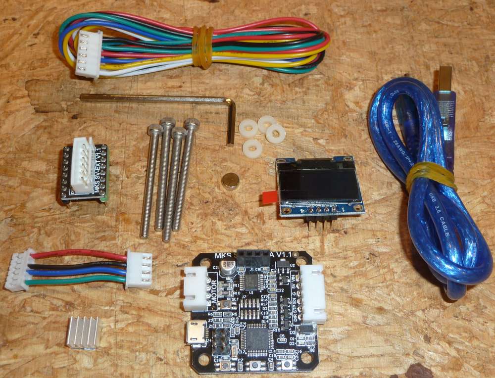
The board is missing the MCU programmer pins, so I presume the MCU is already programmed with at least a bootloader and most likely the full closed loop driver software.
-
@NeverDie I could actually try this out.
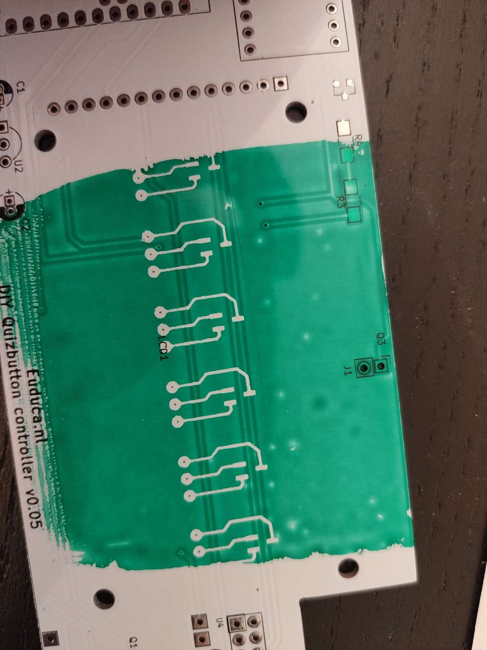
I recently received solder mask paint, both white and green.
And I have a cheap 3 Chinese Watts uv laser engraver.
I was thinking that using transparent sheets is the easiest way to go since you have to expose it anyway, but ofcourse that also means more material use.
@Joerideman said in CNC PCB milling:
@NeverDie I could actually try this out.
I recently received solder mask paint, both white and green.
And I have a cheap 3 Chinese Watts uv laser engraver.
I was thinking that using transparent sheets is the easiest way to go since you have to expose it anyway, but ofcourse that also means more material use.
While you're at it, would you please also try selectively curing the solder mask with your uv laser? If that could be done, I think it might be cleaner all around as compared to laser ablating solder mask that's already cured. For one thing, no fumes from burning to contend with. Also, I'm guessing the output power for curing could be less than for burning, and so maybe it would be safer to use for that reason.
On my end I found a 405nm laser on ebay with 600mw output power, with an adjustable focus, a focal length of 1 to 5 inches, and with a focus diameter of less than 100 microns. i.e. <0.01mm. I have no idea whether that's powerful enough to do laser ablation, but maybe?
Is there such a thing as solder mask which is clear to uv light? Anyone know? If not, then I'm guessing the solder mask would have to be applied very thinly, or else the uv light might not be able to penetrate deeply enough toe cure it all the way. So, for that reason, solder mask which is clear to uv light (even after curing) sounds like it would be the best, at least from a curing point of view. From a laser ablation point of view, I presume you would want just the opposite.
Edit: It turns out optically clear solder mask does exist. OSHPark uses it over their black FR4 substrate to create their "after dark" PCB's. Whether it is also clear to uv, though, I have no idea.
-
Hi all,
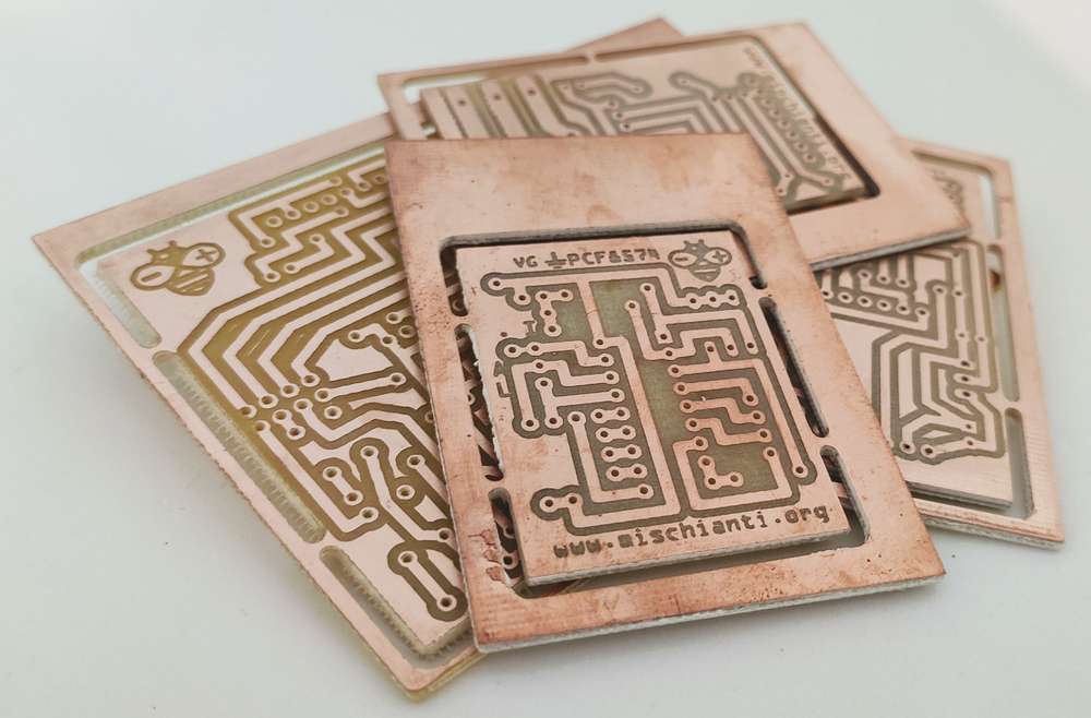
I build my CNC, to do PCB, i started from an old project and I add some addiction and I create the electronic with limit switch probe etc..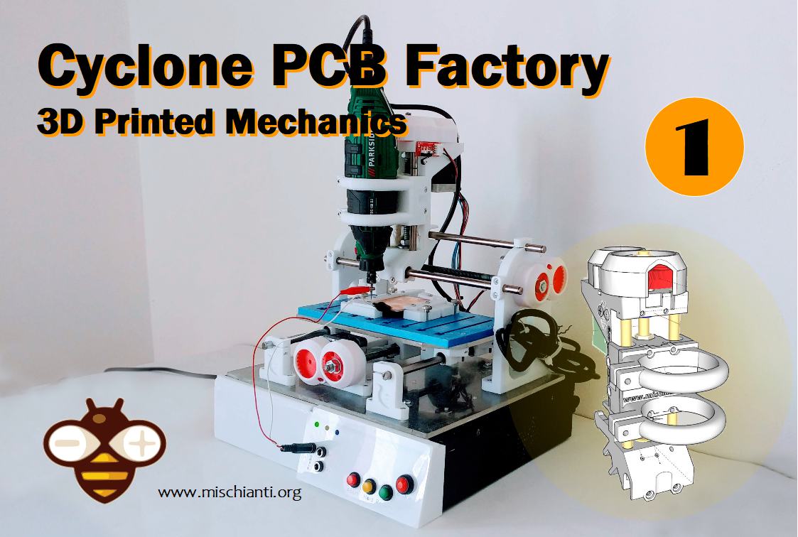
Here my tutorial to build 3D printed CNC
https://www.mischianti.org/category/tutorial/cyclone-pcb-factory-how-to-build-it/And Here the FlatCAM tutorial
https://www.mischianti.org/category/tutorial/flatcam-complete-tutorial/But my first CNC is in my heart :laughing: It's working, and I create a lot of PCB with that...
Naturally It's for home use, but I resolved a lot of situation with that.
Bye RM
-
@NeverDie 100 microns = 0.1mm 1m=1,000milimeters=1,000,000micrometers (microns) 1mm=1,000microns
The UV laser solder mask making has some issues:
- for curing with a laser you need a larger spot, imagine a 0.1mm beam scanning a whole 50x50mm pcb, that takes 500 passes to cover the whole board at 0.1mm resolution. A slightly out of focus laser with 0.3mm beam is more likely to get the job done faster and more uniform. To get the best results using cheap kinematics is best to "scan" the board with some margins for acceleration and deceleration, any attempt at vector cutting the shapes results in a lot of positional error due to backlash and slacks in the kinematics of these kind of laser.
- reflections, the stronger the uv the more it will flare and reflect and the reflections will cure adiacent regions, maybe some which should not get cured, a weak laser is preferred, 50mW or even less, to reduce flaring and reflections.
- burning away already cured paint.... I don't really know if it's possible, the UV paint is made to get cured by UV, not burned, you either need a very strong laser or a different wavelength, maybe CO2 laser. I happen to have a CO2 40W laser but never tried to burn already cured solder mask away.
- focusing and perpendicularity, a slightly not perpendicular beam has an oval shape and the vertical/horizontal size is thrown off, also slight height differences in substrate can and will make the focus spot bigger/smaller as the beam is a cone and you intersect it higher or lower.
LE. I would get an EleksMaker 405nm 500mw laser and start from there. https://www.banggood.com/EleksMaker-EL01-500-405nm-500mW-Blue-Violet-Laser-Module-PWM-Modulation-2_54-3P-DIY-Engraver-p-1287791.html?rmmds=search&cur_warehouse=CN
-
I just started with my first UV mask experience.
Following a YouTube video about how to apply the paint. I use a transparent sheet anyway to put the paint on. If I had printed the pads on there before exposing than my only task would have been to rinse it after a minute.
Either way, first test to apply it failed. Better cleaning next time.
So far... I find it difficult to apply the paint. And I find it difficult to expose the paint and then remove it again.
Edit: I have already reached the tenth test. So I am starting to root for the laser. although aligning will be very difficult.
Edit again: Exposing uv paint is problematic. It worked a bit, but I think I will have to experiment with curing times. It is far less forgiving than exposing pcb's. On the other hand... I now understand why they use there mill for this.
I am a bit out of material to put the paint on, and out of patience. The laser will have to come later. I am not so experienced yet using that thing. It takes a bit of time to set it up.
@Joerideman said in CNC PCB milling:
I just started with my first UV mask experience.
Following a YouTube video about how to apply the paint. I use a transparent sheet anyway to put the paint on. If I had printed the pads on there before exposing than my only task would have been to rinse it after a minute.
Either way, first test to apply it failed. Better cleaning next time.
So far... I find it difficult to apply the paint. And I find it difficult to expose the paint and then remove it again.
Edit: I have already reached the tenth test. So I am starting to root for the laser. although aligning will be very difficult.
Edit again: Exposing uv paint is problematic. It worked a bit, but I think I will have to experiment with curing times. It is far less forgiving than exposing pcb's. On the other hand... I now understand why they use there mill for this.
I am a bit out of material to put the paint on, and out of patience. The laser will have to come later. I am not so experienced yet using that thing. It takes a bit of time to set it up.
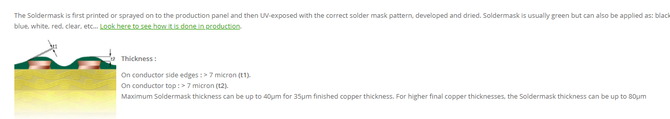
You might want to try a drawdown bar to get a precise, uniform, and repeatable (!) film thickness:

There are different types of coating bars. Some have adjustable heights. They all work on the same principle. You'd have to account for the height of your PCB, instead of the height of paper or a drawdown card, but aside from that it should work the same. They are essentially screeds. You probably want to aim for a thickness above the copper of about 0.5mm. I've seen youtube videos where people try to achieve that by just eyeballing it, but good luck with that.
-
Hi all,
I build my CNC, to do PCB, i started from an old project and I add some addiction and I create the electronic with limit switch probe etc..
Here my tutorial to build 3D printed CNC
https://www.mischianti.org/category/tutorial/cyclone-pcb-factory-how-to-build-it/And Here the FlatCAM tutorial
https://www.mischianti.org/category/tutorial/flatcam-complete-tutorial/But my first CNC is in my heart :laughing: It's working, and I create a lot of PCB with that...
Naturally It's for home use, but I resolved a lot of situation with that.
Bye RM
@Renzo-Mischianti Thanks for your post. Looks like you've been quite a busy bee. ;-)
Have you had any success with solder mask? -
@Joerideman said in CNC PCB milling:
I just started with my first UV mask experience.
Following a YouTube video about how to apply the paint. I use a transparent sheet anyway to put the paint on. If I had printed the pads on there before exposing than my only task would have been to rinse it after a minute.
Either way, first test to apply it failed. Better cleaning next time.
So far... I find it difficult to apply the paint. And I find it difficult to expose the paint and then remove it again.
Edit: I have already reached the tenth test. So I am starting to root for the laser. although aligning will be very difficult.
Edit again: Exposing uv paint is problematic. It worked a bit, but I think I will have to experiment with curing times. It is far less forgiving than exposing pcb's. On the other hand... I now understand why they use there mill for this.
I am a bit out of material to put the paint on, and out of patience. The laser will have to come later. I am not so experienced yet using that thing. It takes a bit of time to set it up.
You might want to try a drawdown bar to get a precise, uniform, and repeatable (!) film thickness:
There are different types of coating bars. Some have adjustable heights. They all work on the same principle. You'd have to account for the height of your PCB, instead of the height of paper or a drawdown card, but aside from that it should work the same. They are essentially screeds. You probably want to aim for a thickness above the copper of about 0.5mm. I've seen youtube videos where people try to achieve that by just eyeballing it, but good luck with that.
@NeverDie for lack of such a roll I have tried another idea I found on YouTube.
I used my laminator to spread out the paint. It gives not that perfect result that you see on factory prints but I was able to expose it for 30s and then a minute of cleaning and then another 2 minutes of exposing.
It is a very solid and well formed layer. Very scratch resistant.
I will have another go on the other side to see if this is repeatable.
Edit:
This is very repeatable. I tried scrubbing with alcohol first but aceton might be a bit better.
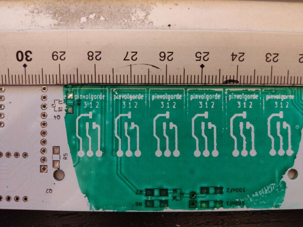
The letters are less than 0,4mm wide.
After scrubbing I exposed everything for another 3 minutes and than it seems to be scratch resistant.
So while I have not yet tested laser exposure or laser engraving, I have now tested a potential reliable way of applying the paint.
-
@NeverDie for lack of such a roll I have tried another idea I found on YouTube.
I used my laminator to spread out the paint. It gives not that perfect result that you see on factory prints but I was able to expose it for 30s and then a minute of cleaning and then another 2 minutes of exposing.
It is a very solid and well formed layer. Very scratch resistant.
I will have another go on the other side to see if this is repeatable.
Edit:
This is very repeatable. I tried scrubbing with alcohol first but aceton might be a bit better.
The letters are less than 0,4mm wide.
After scrubbing I exposed everything for another 3 minutes and than it seems to be scratch resistant.
So while I have not yet tested laser exposure or laser engraving, I have now tested a potential reliable way of applying the paint.
@Joerideman Looks promising.
What is it that you put down on top of the solder mask before putting it into the laminator? I guess some kind of acetate with a black uv mask printed on it?
How many passes through the laminator?
-
@Joerideman said in CNC PCB milling:
I just started with my first UV mask experience.
Following a YouTube video about how to apply the paint. I use a transparent sheet anyway to put the paint on. If I had printed the pads on there before exposing than my only task would have been to rinse it after a minute.
Either way, first test to apply it failed. Better cleaning next time.
So far... I find it difficult to apply the paint. And I find it difficult to expose the paint and then remove it again.
Edit: I have already reached the tenth test. So I am starting to root for the laser. although aligning will be very difficult.
Edit again: Exposing uv paint is problematic. It worked a bit, but I think I will have to experiment with curing times. It is far less forgiving than exposing pcb's. On the other hand... I now understand why they use there mill for this.
I am a bit out of material to put the paint on, and out of patience. The laser will have to come later. I am not so experienced yet using that thing. It takes a bit of time to set it up.
You might want to try a drawdown bar to get a precise, uniform, and repeatable (!) film thickness:
There are different types of coating bars. Some have adjustable heights. They all work on the same principle. You'd have to account for the height of your PCB, instead of the height of paper or a drawdown card, but aside from that it should work the same. They are essentially screeds. You probably want to aim for a thickness above the copper of about 0.5mm. I've seen youtube videos where people try to achieve that by just eyeballing it, but good luck with that.
@NeverDie said in CNC PCB milling:
You probably want to aim for a thickness above the copper of about 0.5mm
Correction: I should have said 0.5 mils.
That's according to altium: https://resources.altium.com/p/how-choose-correct-solder-mask-your-pcb#:~:text=The typical solder mask thickness,solder mask over your traces.
However, I'm not sure if they're referring to wet film thickness or dry film thickness. I guess with uv cured paint it maybe would be the same either way?
-
@Joerideman Looks promising.
What is it that you put down on top of the solder mask before putting it into the laminator? I guess some kind of acetate with a black uv mask printed on it?
How many passes through the laminator?
You know I was just considering if it was worth it to film the process. But I think this will be a bit to much work. I will have to at least clear my desk for it to be presentable :-).
I but the PCB in a polypropylene A4 sized folder. It is thin material and the paint does not really want to stick on it.
The transparent sheets I use for printing the design on are made for inkjet printers. The paint sticks very well to this so the Polypropylene is very important.
Than only once I let it go trough the laminator. I have to make sure that it actually goes through it does not really want to on it's own.
-
You know I was just considering if it was worth it to film the process. But I think this will be a bit to much work. I will have to at least clear my desk for it to be presentable :-).
I but the PCB in a polypropylene A4 sized folder. It is thin material and the paint does not really want to stick on it.
The transparent sheets I use for printing the design on are made for inkjet printers. The paint sticks very well to this so the Polypropylene is very important.
Than only once I let it go trough the laminator. I have to make sure that it actually goes through it does not really want to on it's own.
@Joerideman So, I presume the uv mask with your printing and artwork goes on top of the polypropylene folder cover? If so, maybe that accounts for the little bit of the fuzziness.
I found a drawdown bar for the prescribed 0.5 mil thickness, but it's not cheap:
https://www.byk-instruments.com/us/en/Physical-Properties/Paint-Application/Manual-Film-Applicators/Bird-Type-Film-Applicators/Single-Bar-6"%2C-0-5-mils/p/5561
Maybe there's something cheaper from China.If your PCB had enough margin on it, then the drawdown bar could index the 0.5 mil height directly to the PCB, which might be the easiest for this type of screeding.
-
@Joerideman So, I presume the uv mask with your printing and artwork goes on top of the polypropylene folder cover? If so, maybe that accounts for the little bit of the fuzziness.
I found a drawdown bar for the prescribed 0.5 mil thickness, but it's not cheap:
https://www.byk-instruments.com/us/en/Physical-Properties/Paint-Application/Manual-Film-Applicators/Bird-Type-Film-Applicators/Single-Bar-6"%2C-0-5-mils/p/5561
Maybe there's something cheaper from China.If your PCB had enough margin on it, then the drawdown bar could index the 0.5 mil height directly to the PCB, which might be the easiest for this type of screeding.
@NeverDie
Ah yes the artwork comes on top of that.I measured the paint thickness with a topcraft caliper. It shows 0,05mm or around 2 mils.
Even if you do manage to get that perfect layer thickness. There might still be the problem of the paint sticking to the artwork more than to the PCB.
This might be different though if the layer is thinner.
I think I can live with how fuzzy it is.
https://youtu.be/T56wuO43lW4
The linked video shows how to make a rod. -
@NeverDie
Ah yes the artwork comes on top of that.I measured the paint thickness with a topcraft caliper. It shows 0,05mm or around 2 mils.
Even if you do manage to get that perfect layer thickness. There might still be the problem of the paint sticking to the artwork more than to the PCB.
This might be different though if the layer is thinner.
I think I can live with how fuzzy it is.
https://youtu.be/T56wuO43lW4
The linked video shows how to make a rod.Yeah, the fuzziness isn't bad at all.
@Joerideman said in CNC PCB milling:
https://youtu.be/T56wuO43lW4
The linked video shows how to make a rod.Thanks for the link. Interesting. Hadn't heard of this technique before. I would have thought that the wire would create artifacts.
All the drawdown bars I'm familiar with are completely smooth. No wires.
-
@NeverDie
Ah yes the artwork comes on top of that.I measured the paint thickness with a topcraft caliper. It shows 0,05mm or around 2 mils.
Even if you do manage to get that perfect layer thickness. There might still be the problem of the paint sticking to the artwork more than to the PCB.
This might be different though if the layer is thinner.
I think I can live with how fuzzy it is.
https://youtu.be/T56wuO43lW4
The linked video shows how to make a rod.@Joerideman said in CNC PCB milling:
I measured the paint thickness with a topcraft caliper. It shows 0,05mm or around 20 mils.
By my rekoning, 0.05mm equals about 2 mils, not 20, since 1 mil = 0.001" by definition. Given how you got there, that's pretty close to the target! Did it cure all the way through? Maybe the 0.5mil spec quoted by Altium is just a minimum value.
It looks as though PCB fabs may actually spray it on:
https://www.eurocircuits.com/sm-solder-mask/
and so they spray it on thicker if the copper laminate is thicker. On top of that, being an industrial process they're probably tuned to spray on the least amount that will still get the job done (to save material cost), so I'm not sure how much we can extrapolate from their metrics.Without other references, but recognizing their profit motive, I'm inclined to take their 0.5 mil as a minimum thickness. The question then is: what can be the maximum thickness and have it still work out well? i.e. still cure all the way through. If the troughs were deep enough, maybe you wouldn't even need a solder paste template: perhaps you could just squeegee on the solder paste to fill the voids left in the solder mask and squeege off the rest? Since with our process we're screeding it on rather than spraying it on, maybe that's an option we have that the professional fabs can't match. If it were possible, it would be a nice two-for-one bonus: solder mask and solder paste template all-in-one!
Edit: As another datapoint, dynamask comes in a 3mil and 4 mil thickness. In their case, though, it says they use a polyethelene release film instead of the polypropylene you're having good luck with:
Dynamask 5000 series film is a transparent, high gloss forest green material which is supplied in
thicknesses of 75 microns (3mils) and 100 microns (4 mils) the film is supplied in several widths and a roll
length of 100 mtrs.
Like most other dry film products the photopolymer is sandwiched between a 25 micron(1.0mil) polyester
support sheet and a 25 micron (1mil) polyethylene release sheet..
https://www.ebay.com/itm/Dry-film-solder-Dynamsk-5000-0-3m-x-1m-/282595757649I ordered some dynamask yesterday just to give it a try, but it will take 2 or 3 weeks to get here.
Lots of interesting recommendations in their instructions. Definitely worth a read. For instance, it looks as though they recommend the copper should be cleaned with hydrochloric acid, and then they want you to scratch it up with pumice. so that the scratches score to a depth of 2 to 4 microns. I presume the aim is to clear away corrosion and to give the dynamask something to key into and help it stick. Maybe the same would also help with getting the Mechanics uv paint to stick to the copper in preference to whatever release sheet is being used, so that it's less likely to peel off with the release sheet. Assuming the mask is fully cured, then if it's a tug-of-war, the stronger bond wins.
They also recommend vacuum lamination over rolled lamination to avoid air bubbles. Of course, they're stating an ideal. Maybe putting it into a vacuum chamber for a while before roller laminating it would be a compromise. Or maybe I should sell my vacuum chamber and use the money to buy a vacuum laminator from aliexpress. On first look there are quite a few which aren't super expensive, although they're still multiples of what a cheap hot roller laminator would cost. @Joerideman It's hard to tell from your photos: did you find that air bubbles were a problem at all using the Mechanics uv solder mask paint?
Edit: Inspired by @Joerideman I ordered a couple different polypropylene sleeves:
https://smile.amazon.com/gp/product/B083LN26WD/ref=ppx_yo_dt_b_asin_title_o00_s00?ie=UTF8&psc=1
which advertise being "non-stick"and some much thicker:
https://smile.amazon.com/gp/product/B07C28PPL6/ref=ppx_yo_dt_b_asin_title_o00_s00?ie=UTF8&psc=1Unfortunately, they aren't due to arrive until Monday.
Meanwhile I'll try to figure out if there are any easily available abrasives or grits that are the equal of the "3F brush pumice" recommended by dynamask for scratching up a PCB's copper.
Edit: looks as though 2000-3000 grit sand paper would be roughly equivalent. Due to the unfortunate way grits are defined (where 20% of the particles can be larger than the nominal grit size), it's probably better to start with 3000 or 2500 grit. Maybe better would be to use something like 3M Trizact, where the abrassive particles are of a more uniform size.
-
In my experiments the best results I got were using a rubber roller with a handle, the film is 0.1-0.2mm thick but that is no problem for the home made led uv exposure box to cure. Here is something similar, unfortunetly mine got lost a while ago when moving out.

I clean the boards after milling with some Scotch Brite metal sponge and the abrasive part of a dish washing Scotch Brite sponge, this also removes the small burs along milled traces. Wash with some IPA in the end and the paint gets good adhesion to the board.The hurdles of getting the uv mask aligned, printed dark enough (damn these new eco printers) makes me want to build a laser for doing this kind of curing. I've just saw a great video of a UV laser using a spinning mirror from a printer, that would make the scanning of the board so much faster.
-
In my experiments the best results I got were using a rubber roller with a handle, the film is 0.1-0.2mm thick but that is no problem for the home made led uv exposure box to cure. Here is something similar, unfortunetly mine got lost a while ago when moving out.
I clean the boards after milling with some Scotch Brite metal sponge and the abrasive part of a dish washing Scotch Brite sponge, this also removes the small burs along milled traces. Wash with some IPA in the end and the paint gets good adhesion to the board.The hurdles of getting the uv mask aligned, printed dark enough (damn these new eco printers) makes me want to build a laser for doing this kind of curing. I've just saw a great video of a UV laser using a spinning mirror from a printer, that would make the scanning of the board so much faster.
@executivul Do you put down something over the paint (such as plastic, for instance) before rolling over it, or do you roll directly over the wet paint with the roller itself?
-
@executivul Do you put down something over the paint (such as plastic, for instance) before rolling over it, or do you roll directly over the wet paint with the roller itself?
@NeverDie I put a piece of clear "document wrap foil"

-
It makes sense. AFAIK, the uv solder mask paint isn't benefited from the laminator heat, just the uniform squeezing from the rollers.
-
The stack goes like this:
-glass
-normal printer paper made transparent to UV light (https://www.amazon.co.uk/Kontakt-chemie-Transparent-21-Spray-200ml/dp/B00ID6KY4K)
-toner (the image is mirrored and placed toner face down)
-transparent film from "document wraps"
-UV solder mask paint
-pcb
-glassThe top and bottom glass pieces are held tight by some binder clips.