CNC PCB milling


  • Mod

    @NeverDie EtherCAT requires a dedicated ASIC (e.g. Beckhoff ET1100) or FPGA IP Core.
    There have been some developments where MPU & EtherCAT slave controller were integrated into a single piece of silicon (TI, Renesas, Microchip) but these are less popular than the ET1100.
    For distributed IO it is an awesome technology, but when all IO and controller can be located onto a single board (like with most hobby CNCs) it is overkill, at least for the masses.
    But again, you never know what nice lowcost EtherCAT solution could be coming our way.


  • Hero Member

    @Yveaux That makes sense to me. If people are mainly doing it for noise immunity, I'm reasonably sure that differential op-amps (which are cheap) and twisted pair wiring (which is cheap) will do the business. That's how ethernet does it. If that's still not enough, then add shielding. Also, the more twisting the better. At least, I would think that it would be sufficient for a home environment.

    I'll be testing this theory with the closed-loop stepper drivers that I'll be installing, since with those it will be the data coms between the GRBL board and the stepper drivers that will be running across long wires instead of power pulses to the steppers, where noise didn't really matter. I guess we'll see!


  • Hey, I have trouble understanding the last 10 posts.

    It sounds like this go's beyond the PCB milling?

    What are you aiming to achieve?


  • Hero Member

    @Joerideman said in CNC PCB milling:

    Hey, I have trouble understanding the last 10 posts.

    It sounds like this go's beyond the PCB milling?

    What are you aiming to achieve?

    No, the aim is still pcb milling. More specifically: PCB milling at fine pitch and whatever might support that. Regular through-hole milling is something that just about any PCB mill can handle, so the discussion has shifted to milling for newer SMD parts, where the pitch between pads can be quite challenging for some mills, like mine for example. Then the question becomes: which are the best bang/buck upgrades (or even just calibrations) that will get you there.


  • So, I have seen that with a popular 3018 CNC a atmega328p-au can be milled.

    0.2mm traces with 0.2mm clearance can be routed.

    What specs are you going for?


  • Hero Member

    @Joerideman said in CNC PCB milling:

    So, I have seen that with a popular 3018 CNC a atmega328p-au can be milled.

    0.2mm traces with 0.2mm clearance can be routed.

    What specs are you going for?

    I thought the atmega328p had wider pitch than that, as I have etched those before. Nonethmeless, where did you see a 3018 that could do those specs? I think for now, if I'm understanding you correctly, that would be good enough, at least for me. That would effectively be a 0.4mm pitch, right? Measured center to center from one pad to the next.

    I don't think my rig is any worse than a 3018. Most low-end CNC's seem pretty similar, with aluminum extrusion frames, acme screws, round rods and inexpensive linear bearings for glides, and dubious spindles, dodgy collets, and questionable z-axis reinforcement against twisting. I guess one could look at bantam tools or wegstr for differences, as they seem to be hitting it. I doubt there's any one thing but probably a range of things done right. Perhaps being companies allows them to source parts reliably with the right tolerances, thus avoiding aliexpress roulette.

    Anyhow, I think I'll get there if I keep chipping away at it. With PCB deliveries slowing down due to covid19, it's worth the effort to figure it out. 😉

    I see working with PCB's as an advantage, because the machine itself doesn't need to be big, and in theory even (some) premium parts become affordable because the travel distances are relatively short.


  • @NeverDie

    I shared a link to this channel before.

    CNC PCB - high quality with the budget 3018 CNC – 05:20
    — DIY TECH BROS

    I am waiting for their next video. I am told it will show us a bit more about the limits of the machine.

    It doesn't actually show an atmege328 I am not sure where or if have actually seen this.

    The Wegstr, has only a Z axis for the spindle. And from what I read they use a brushless motor for this. I guess that by only moving it up and down, this part becomes very rigid.


  • Hero Member

    @Joerideman said in CNC PCB milling:

    @NeverDie

    I shared a link to this channel before.

    CNC PCB - high quality with the budget 3018 CNC – 05:20
    — DIY TECH BROS

    I'm pretty sure the pitch on the given example in that video is wider than 0.4mm.

    The Wegstr, has only a Z axis for the spindle. And from what I read they use a brushless motor for this. I guess that by only moving it up and down, this part becomes very rigid.

    Good observation. The fixed z-axis is closer to a classic mill configuration. I like that approach because it makes it easier to build rigidity into the z-axis.


  • Hero Member

    @Joerideman said in CNC PCB milling:

    So, I have seen that with a popular 3018 CNC a atmega328p-au can be milled.

    0.2mm traces with 0.2mm clearance can be routed.

    What specs are you going for?

    I looked up the atmega328p datasheet here: http://ww1.microchip.com/downloads/en/DeviceDoc/Atmel-7810-Automotive-Microcontrollers-ATmega328P_Datasheet.pdf

    The pitch on the DIP package is obviously 2.540mm.

    The pitch on the TQFP package is 0.8mm. That's the one I tend to favor because it's easy to handle, and I have a clamshell chip programmer for it.

    The ptich on the VQFN package is 0.5mm.

    On the other hand, looking at the "other' datasheet for the atmega328p: https://ww1.microchip.com/downloads/en/DeviceDoc/ATmega48A-PA-88A-PA-168A-PA-328-P-DS-DS40002061A.pdf
    it does appear to also make reference to a 28M1 package, which has only 28 pins and a lead pitch of 0.45mm. As far as the atmega328p is concerned, that appears to be the lowest pitch package. Pad width is a nominal 0.22mm, so of the various packages it's the closest to the one you said. The entire package is just 4mmx4mm in size.

    I'd be reluctant to attempt a chip that small without solder mask, but with an appropriate solder mask it would be possible I suppose. Hence, getting the solder mask part of pcb milling right is definitely important as the line pitch gets smaller and smaller, and that certainly is the trend.

    In any case, the lead pitch on the nRF52832 is 0.4mm, so there's definitely a need to accurately etch that pitch. I seem to recall running into components with even lower lead pitch than that, but offhand I can't remember which components those were.


  • Hero Member

    On another thread (https://forum.mysensors.org/topic/10812/the-harvester-ultimate-power-supply-for-the-raybeacon-dk/211?_=1598132652123) we were talking about using a laser to directly etch the copper clad on a PCB, which I think would be hard to do without a fiber laser. Nonetheless, it just now occurred to me that using a regular etching laser might be just the ticket to use for removing black solder mask over solder pads, precisely because it would fail at removing the copper underneath. After all, many people are already using this technique for removing cheap black paint (used as an acid etching mask) from copper PCBs, so I presume it would work equally well for selectively removing black solder mask? At least to me, this sounds extremely promising.


  • @NeverDie Yeah, it's a very interesting option! Similar approach might be to use a UV printer. The UV paint is known to be resistant to FeCl3 and hence results in nice and clean edges. But that's subject of paint and a laser engraver could be used over UV paint too.

    On the other hand, a fiber laser might be a nice all-in-one solution. It can do the PCB routing, can cut the board edges, and drill everything in one pass. After that, the same device can be used to manufacture solder mask using a kapton tape and also engrave the silk layer on top of it. Finally, it can cut stencils.

    The only missing part is the through hole plating. I still have concern that laser drilled the edges will be good enough for metalization, this has to be checked. But a previously drilled and plated board is much easier to etch with laser rather than a milling machine.


  • Hero Member

    @Mishka said in CNC PCB milling:

    @NeverDie Yeah, it's a very interesting option! Similar approach might be to use a UV printer. The UV paint is known to be resistant to FeCl3 and hence results in nice and clean edges. But that's subject of paint and a laser engraver could be used over UV paint too.

    On the other hand, a fiber laser might be a nice all-in-one solution. It can do the PCB routing, can cut the board edges, and drill everything in one pass. After that, the same device can be used to manufacture solder mask using a kapton tape and also engrave the silk layer on top of it. Finally, it can cut stencils.

    The only missing part is the through hole plating. I still have concern that laser drilled the edges will be good enough for metalization, this has to be checked. But a previously drilled and plated board is much easier to etch with laser rather than a milling machine.

    Somewhere out there is a product (it has a youtube video) where you pull a special paste through the via's under a vacuum and then do regular electroplating to get your vias plated. It's meant for DIY.

    I wonder if you could just squeegee fine grained solder paste into the vias and then heat it up to make the connections? I suppose you'd want to do it after the solder mask phase. If the vias are big enough, I don't see why this wouldn't work. In the worst case it might take more than one pass, and it might also have the advantage of "tinning" your regular solder pads.


  • Here is a fiber laser machine example: https://mylasermart.com/product/ultra-high-speed-laser-machine/

    It uses 50W fiber laser. Minimal track width is 0.05 mm! Space between tracks is 0.025 mm which is limited by the beam size. Precision ±2 µm.

    This particular one doesn't look any cheap, but it gives the strong hint what to look for.


  • Hero Member

    @Mishka The company best known for direct laser etching of PCBs is called LPKF. If cost is no barrier, they've got great solutions that they can ship you today. Lots of impressive youtube videos about their products. If mylasermart, or anybody else, can do the same or similar for a lot less though, it would certainly be interesting.


  • Hero Member

    @Mishka said in CNC PCB milling:

    @NeverDie Yeah, it's a very interesting option! Similar approach might be to use a UV printer. The UV paint is known to be resistant to FeCl3 and hence results in nice and clean edges. But that's subject of paint and a laser engraver could be used over UV paint too.

    On the other hand, a fiber laser might be a nice all-in-one solution. It can do the PCB routing, can cut the board edges, and drill everything in one pass. After that, the same device can be used to manufacture solder mask using a kapton tape and also engrave the silk layer on top of it. Finally, it can cut stencils.

    The only missing part is the through hole plating. I still have concern that laser drilled the edges will be good enough for metalization, this has to be checked. But a previously drilled and plated board is much easier to etch with laser rather than a milling machine.

    Maybe UV printers are worth another look. I've searched in the past for flatbed UV inkjet printers but almost everything I found was commercially oriented toward print shops, and the prices were basically $2,000 and up. I suppose one option is to actually go to a local print shop and use theirs and pay a per-use fee. There do exist some battery operated hand-held units that you can sorta "wipe" across a surface and it will print as you go with uv ink. Those are a lot cheaper, and maybe they could be adapted.... but that's a project I'd rather avoid.

    You'd think that comparatively inexpensive 3D resin printers could be tricked into doing it.

    Anyhow, keep the ideas coming! Brainstorming works better that way.


  • Hero Member

    @NeverDie Not surprisingly, some people are already doing laser ablation of soldermask, and the results are pretty good!
    Lasering out PCB Solder Mask in ChiliPeppr – 07:39
    — John Lauer


  • Hero Member

    While I wait for the closed loop drivers to arrive, I attached these fancy copper heatsinks to DRV8825 drivers using artic silver thermally conductive epoxy.
    heatsinks.JPG
    It makes for a permanent attachment, but from what I've read, this should allow them to be driven at their maximum rated current without overheating. This way I'll at least have a glimpse of what it's like to run the steppers at 45v with 2.1a current before switching over to the 24v volt closed loop drivers. I'll let the epoxy fully cure overnight and then give them a test drive tomorrow. It might (?) even turn out that with the extra power I don't even need the closed loop drivers. We'll see.

    I loaded GRBL 1.1h onto the arduino. Doing so is a very simple and quick process: just copy the GRBL library over to the arduino library folder and then compile and upload the uploadGRBL example program that comes with it. That's all there is to it. From there the default settings can be customized if so desired. I'll probably be testing different speed and acceleration settings.


  • Hero Member

    @NeverDie said in CNC PCB milling:

    @NeverDie Not surprisingly, some people are already doing laser ablation of soldermask, and the results are pretty good!
    Lasering out PCB Solder Mask in ChiliPeppr – 07:39
    — John Lauer

    I tried shopping for lasers last night, but it's not straight forward. The variables seem be: power, wavelength, focal distance, optics, size of dot, and sharpness of dot. Unfortunately, lasers don't seem to be marketed that way. Instead, the listings seem to assume you can infer that.
    Apparently single mode lasers would be better for this application because they produce better defined dots, but that's the only tidbit of useful information I've so far gleaned. If anyone here with laser experience can make a recommendation for a CNC mountable laser to ablate solder mask, that would be great. Also, is it better to steer the beam by moving the laser around on the CNC as though it were and endmill, or is it better to get a laser with moveable mirrors to direct the beam where it should go? I'm guessing that treating it like an endmill would be the more plug-and-play of the two options, where you simply turn on the laser whenever the z-axis gcode implies the z-axis is below zero, and turn it off when the gcode implies the z-axis would be above zero.


  • @NeverDie I could actually try this out.

    I recently received solder mask paint, both white and green.

    And I have a cheap 3 Chinese Watts uv laser engraver.

    I was thinking that using transparent sheets is the easiest way to go since you have to expose it anyway, but ofcourse that also means more material use.


  • Hero Member

    @Joerideman said in CNC PCB milling:

    @NeverDie I could actually try this out.

    I recently received solder mask paint, both white and green.

    And I have a cheap UV laser engraver.

    That would be great!


  • Hero Member

    @NeverDie said in CNC PCB milling:

    @NeverDie said in CNC PCB milling:

    I suppose the GRBL capacitor rating may soon be a moot issue anyway, as the servo42A closed loop driver accepts an input voltage of only 12-24v, and, not surprisingly, it appears to have its own back EMF cap on its driverboard:
    alt text

    The original mechaduino v0.2 accepted up to 35v:
    mechaduino_voltage.png

    So, because the clone that I purchased allows for only 24v input, it's an unfortunate downgrade from the original. 😞

    Reporting back: it turns out the voltage issue is moot. After playing around with a NEMA 17 and a DRV8255 driver, it turns out the NEMA 17 doesn't behave well at higher voltages anyway. At the higher voltages it's prone to resonating and not even turning. Also, unlike the original NEMA 17's, the "upgraded" NEMA 17's don't seem to perform well at 12v either. Rather, 24v seems to be more or less the sweet spot, and at a current that's around a little more half its rated maximum. So that was quite a surprise, at least to me. Also, even with the copper finned heatsinks, and the reduced voltages and currents, the DRV8255's get quite hot! If I'm going to run the upgraded steppers from stepsticks, I think I'm probably going to need to fan cooling in addition to the heatsinks. I wonder if I'll have to add some kind of heatsinks and fan cooling to the closed loop steppers as well?

    I guess, if need be, I could either "downgrade" back to the original, smaller NEMA 17's that came with the kit, or else upgrade to TMC5160's (which run cooler) to better support the higher torque "upgraded" NEMA 17's. In the worst case I would shift to the standalone drivers discussed earlier, each of which comes with massive heatsinks.

    All that said, the present currents are fairly paltry compared to what NEMA 23's consume. I imagine NEMA 23 drivers get very hot indeed!


    Lastly, but importantly, I think I maybe see why my setup is loosing positioning when I jog around manually. Basically, by default GRBL turns off the drivers almost completely at the end of a command rather than maintaining holding torque on them. I'm guessing that may allow some slippage to happen that shouldn't happen during those relaxation periods. It has me curious now as to whether this might also happen while running a lengthy grbl script--maybe during periods when the z-height is locked and not otherwise changing? I guess I'll have to run some tests to find out. I find it hard to believe that GRBL might make a bonehead mistake like that, but.... maybe? Regardless, this would be something that the closed loop drivers could correct for, because their magnetic encoders have quite good resolution. 🙂 Based on tracking info, I'm pretty sure I'll be receiving them this week.


  • Hero Member

    I never imagined that I would burn out four (4) DRV8825 stepper drivers and two (2) arduinos in just a short stretch of time. Something about this GRBL design makes it ridiculously fragile. And, by the way, the fuse never blew! 😜 It really might as well be a piece of wire for all the good it's doing. I'm just glad it didn't fry the computer I have connected to it.

    Edit: Good heavens! Here's a similar board, and beware! It's absolutely riddled with fatal flaws:
    Worst CNC shield 12v /24 volt board GRBL v4 Arduino Nano (Problems, fix, Mods, flaws, corrections) – 10:16
    — MangoJelly Solutions for FreeCAD


  • Hero Member

    I received the closed loop drivers. It contains a good amount of kit for making the upgrade:
    kit.JPG

    The board is missing the MCU programmer pins, so I presume the MCU is already programmed with at least a bootloader and most likely the full closed loop driver software.


  • Hero Member

    @Joerideman said in CNC PCB milling:

    @NeverDie I could actually try this out.

    I recently received solder mask paint, both white and green.

    And I have a cheap 3 Chinese Watts uv laser engraver.

    I was thinking that using transparent sheets is the easiest way to go since you have to expose it anyway, but ofcourse that also means more material use.

    While you're at it, would you please also try selectively curing the solder mask with your uv laser? If that could be done, I think it might be cleaner all around as compared to laser ablating solder mask that's already cured. For one thing, no fumes from burning to contend with. Also, I'm guessing the output power for curing could be less than for burning, and so maybe it would be safer to use for that reason.

    On my end I found a 405nm laser on ebay with 600mw output power, with an adjustable focus, a focal length of 1 to 5 inches, and with a focus diameter of less than 100 microns. i.e. <0.01mm. I have no idea whether that's powerful enough to do laser ablation, but maybe?

    Is there such a thing as solder mask which is clear to uv light? Anyone know? If not, then I'm guessing the solder mask would have to be applied very thinly, or else the uv light might not be able to penetrate deeply enough toe cure it all the way. So, for that reason, solder mask which is clear to uv light (even after curing) sounds like it would be the best, at least from a curing point of view. From a laser ablation point of view, I presume you would want just the opposite.

    Edit: It turns out optically clear solder mask does exist. OSHPark uses it over their black FR4 substrate to create their "after dark" PCB's. Whether it is also clear to uv, though, I have no idea.


  • Hi all,
    I build my CNC, to do PCB, i started from an old project and I add some addiction and I create the electronic with limit switch probe etc..

    My CNC
    A_set_of_milled_PCB.jpg

    Here my tutorial to build 3D printed CNC
    https://www.mischianti.org/category/tutorial/cyclone-pcb-factory-how-to-build-it/

    And Here the FlatCAM tutorial
    https://www.mischianti.org/category/tutorial/flatcam-complete-tutorial/

    But my first CNC is in my heart 😆 It's working, and I create a lot of PCB with that...

    My first CNC

    Naturally It's for home use, but I resolved a lot of situation with that.

    Bye RM


  • @NeverDie 100 microns = 0.1mm 1m=1,000milimeters=1,000,000micrometers (microns) 1mm=1,000microns

    The UV laser solder mask making has some issues:

    1. for curing with a laser you need a larger spot, imagine a 0.1mm beam scanning a whole 50x50mm pcb, that takes 500 passes to cover the whole board at 0.1mm resolution. A slightly out of focus laser with 0.3mm beam is more likely to get the job done faster and more uniform. To get the best results using cheap kinematics is best to "scan" the board with some margins for acceleration and deceleration, any attempt at vector cutting the shapes results in a lot of positional error due to backlash and slacks in the kinematics of these kind of laser.
    2. reflections, the stronger the uv the more it will flare and reflect and the reflections will cure adiacent regions, maybe some which should not get cured, a weak laser is preferred, 50mW or even less, to reduce flaring and reflections.
    3. burning away already cured paint.... I don't really know if it's possible, the UV paint is made to get cured by UV, not burned, you either need a very strong laser or a different wavelength, maybe CO2 laser. I happen to have a CO2 40W laser but never tried to burn already cured solder mask away.
    4. focusing and perpendicularity, a slightly not perpendicular beam has an oval shape and the vertical/horizontal size is thrown off, also slight height differences in substrate can and will make the focus spot bigger/smaller as the beam is a cone and you intersect it higher or lower.

    LE. I would get an EleksMaker 405nm 500mw laser and start from there. https://www.banggood.com/EleksMaker-EL01-500-405nm-500mW-Blue-Violet-Laser-Module-PWM-Modulation-2_54-3P-DIY-Engraver-p-1287791.html?rmmds=search&cur_warehouse=CN


  • I just started with my first UV mask experience.

    Following a YouTube video about how to apply the paint. I use a transparent sheet anyway to put the paint on. If I had printed the pads on there before exposing than my only task would have been to rinse it after a minute.

    Either way, first test to apply it failed. Better cleaning next time.

    So far... I find it difficult to apply the paint. And I find it difficult to expose the paint and then remove it again.

    Edit: I have already reached the tenth test. So I am starting to root for the laser. although aligning will be very difficult.

    Edit again: Exposing uv paint is problematic. It worked a bit, but I think I will have to experiment with curing times. It is far less forgiving than exposing pcb's. On the other hand... I now understand why they use there mill for this.

    I am a bit out of material to put the paint on, and out of patience. The laser will have to come later. I am not so experienced yet using that thing. It takes a bit of time to set it up.


  • Hero Member

    @Joerideman said in CNC PCB milling:

    I just started with my first UV mask experience.

    Following a YouTube video about how to apply the paint. I use a transparent sheet anyway to put the paint on. If I had printed the pads on there before exposing than my only task would have been to rinse it after a minute.

    Either way, first test to apply it failed. Better cleaning next time.

    So far... I find it difficult to apply the paint. And I find it difficult to expose the paint and then remove it again.

    Edit: I have already reached the tenth test. So I am starting to root for the laser. although aligning will be very difficult.

    Edit again: Exposing uv paint is problematic. It worked a bit, but I think I will have to experiment with curing times. It is far less forgiving than exposing pcb's. On the other hand... I now understand why they use there mill for this.

    I am a bit out of material to put the paint on, and out of patience. The laser will have to come later. I am not so experienced yet using that thing. It takes a bit of time to set it up.

    You might want to try a drawdown bar to get a precise, uniform, and repeatable (!) film thickness:
    alt text

    There are different types of coating bars. Some have adjustable heights. They all work on the same principle. You'd have to account for the height of your PCB, instead of the height of paper or a drawdown card, but aside from that it should work the same. They are essentially screeds. You probably want to aim for a thickness above the copper of about 0.5mm. I've seen youtube videos where people try to achieve that by just eyeballing it, but good luck with that.


  • Hero Member

    @Renzo-Mischianti Thanks for your post. Looks like you've been quite a busy bee. 😉
    Have you had any success with solder mask?


  • @NeverDie for lack of such a roll I have tried another idea I found on YouTube.

    I used my laminator to spread out the paint. It gives not that perfect result that you see on factory prints but I was able to expose it for 30s and then a minute of cleaning and then another 2 minutes of exposing.

    It is a very solid and well formed layer. Very scratch resistant. IMG_20200826_005709.jpg

    I will have another go on the other side to see if this is repeatable.

    Edit:

    This is very repeatable. I tried scrubbing with alcohol first but aceton might be a bit better.

    The letters are less than 0,4mm wide.

    After scrubbing I exposed everything for another 3 minutes and than it seems to be scratch resistant.

    IMG_20200826_012901.jpg

    So while I have not yet tested laser exposure or laser engraving, I have now tested a potential reliable way of applying the paint.


  • Hero Member

    @Joerideman Looks promising.

    What is it that you put down on top of the solder mask before putting it into the laminator? I guess some kind of acetate with a black uv mask printed on it?

    How many passes through the laminator?


  • Hero Member

    @NeverDie said in CNC PCB milling:

    You probably want to aim for a thickness above the copper of about 0.5mm

    Correction: I should have said 0.5 mils.

    That's according to altium: https://resources.altium.com/p/how-choose-correct-solder-mask-your-pcb#:~:text=The typical solder mask thickness,solder mask over your traces.

    However, I'm not sure if they're referring to wet film thickness or dry film thickness. I guess with uv cured paint it maybe would be the same either way?


  • @NeverDie

    You know I was just considering if it was worth it to film the process. But I think this will be a bit to much work. I will have to at least clear my desk for it to be presentable :-).

    I but the PCB in a polypropylene A4 sized folder. It is thin material and the paint does not really want to stick on it.

    The transparent sheets I use for printing the design on are made for inkjet printers. The paint sticks very well to this so the Polypropylene is very important.

    Than only once I let it go trough the laminator. I have to make sure that it actually goes through it does not really want to on it's own.


  • Hero Member

    @Joerideman So, I presume the uv mask with your printing and artwork goes on top of the polypropylene folder cover? If so, maybe that accounts for the little bit of the fuzziness.

    I found a drawdown bar for the prescribed 0.5 mil thickness, but it's not cheap:
    https://www.byk-instruments.com/us/en/Physical-Properties/Paint-Application/Manual-Film-Applicators/Bird-Type-Film-Applicators/Single-Bar-6"%2C-0-5-mils/p/5561
    Maybe there's something cheaper from China.

    If your PCB had enough margin on it, then the drawdown bar could index the 0.5 mil height directly to the PCB, which might be the easiest for this type of screeding.


  • @NeverDie
    Ah yes the artwork comes on top of that.

    I measured the paint thickness with a topcraft caliper. It shows 0,05mm or around 2 mils.

    Even if you do manage to get that perfect layer thickness. There might still be the problem of the paint sticking to the artwork more than to the PCB.

    This might be different though if the layer is thinner.

    I think I can live with how fuzzy it is.

    https://youtu.be/T56wuO43lW4
    The linked video shows how to make a rod.


  • Hero Member

    Yeah, the fuzziness isn't bad at all.

    @Joerideman said in CNC PCB milling:

    https://youtu.be/T56wuO43lW4
    The linked video shows how to make a rod.

    Thanks for the link. Interesting. Hadn't heard of this technique before. I would have thought that the wire would create artifacts.

    All the drawdown bars I'm familiar with are completely smooth. No wires.


  • Hero Member

    @Joerideman said in CNC PCB milling:

    I measured the paint thickness with a topcraft caliper. It shows 0,05mm or around 20 mils.

    By my rekoning, 0.05mm equals about 2 mils, not 20, since 1 mil = 0.001" by definition. Given how you got there, that's pretty close to the target! Did it cure all the way through? Maybe the 0.5mil spec quoted by Altium is just a minimum value.

    It looks as though PCB fabs may actually spray it on:
    solder_mask_thickness.png
    https://www.eurocircuits.com/sm-solder-mask/
    and so they spray it on thicker if the copper laminate is thicker. On top of that, being an industrial process they're probably tuned to spray on the least amount that will still get the job done (to save material cost), so I'm not sure how much we can extrapolate from their metrics.

    Without other references, but recognizing their profit motive, I'm inclined to take their 0.5 mil as a minimum thickness. The question then is: what can be the maximum thickness and have it still work out well? i.e. still cure all the way through. If the troughs were deep enough, maybe you wouldn't even need a solder paste template: perhaps you could just squeegee on the solder paste to fill the voids left in the solder mask and squeege off the rest? Since with our process we're screeding it on rather than spraying it on, maybe that's an option we have that the professional fabs can't match. If it were possible, it would be a nice two-for-one bonus: solder mask and solder paste template all-in-one!


    Edit: As another datapoint, dynamask comes in a 3mil and 4 mil thickness. In their case, though, it says they use a polyethelene release film instead of the polypropylene you're having good luck with:

    Dynamask 5000 series film is a transparent, high gloss forest green material which is supplied in

    thicknesses of 75 microns (3mils) and 100 microns (4 mils) the film is supplied in several widths and a roll

    length of 100 mtrs.

    Like most other dry film products the photopolymer is sandwiched between a 25 micron(1.0mil) polyester

    support sheet and a 25 micron (1mil) polyethylene release sheet..
    https://www.ebay.com/itm/Dry-film-solder-Dynamsk-5000-0-3m-x-1m-/282595757649

    I ordered some dynamask yesterday just to give it a try, but it will take 2 or 3 weeks to get here.

    Lots of interesting recommendations in their instructions. Definitely worth a read. For instance, it looks as though they recommend the copper should be cleaned with hydrochloric acid, and then they want you to scratch it up with pumice. so that the scratches score to a depth of 2 to 4 microns. I presume the aim is to clear away corrosion and to give the dynamask something to key into and help it stick. Maybe the same would also help with getting the Mechanics uv paint to stick to the copper in preference to whatever release sheet is being used, so that it's less likely to peel off with the release sheet. Assuming the mask is fully cured, then if it's a tug-of-war, the stronger bond wins.

    They also recommend vacuum lamination over rolled lamination to avoid air bubbles. Of course, they're stating an ideal. Maybe putting it into a vacuum chamber for a while before roller laminating it would be a compromise. Or maybe I should sell my vacuum chamber and use the money to buy a vacuum laminator from aliexpress. On first look there are quite a few which aren't super expensive, although they're still multiples of what a cheap hot roller laminator would cost. @Joerideman It's hard to tell from your photos: did you find that air bubbles were a problem at all using the Mechanics uv solder mask paint?


    Edit: Inspired by @Joerideman I ordered a couple different polypropylene sleeves:

    https://smile.amazon.com/gp/product/B083LN26WD/ref=ppx_yo_dt_b_asin_title_o00_s00?ie=UTF8&psc=1
    which advertise being "non-stick"

    and some much thicker:
    https://smile.amazon.com/gp/product/B07C28PPL6/ref=ppx_yo_dt_b_asin_title_o00_s00?ie=UTF8&psc=1

    Unfortunately, they aren't due to arrive until Monday.

    Meanwhile I'll try to figure out if there are any easily available abrasives or grits that are the equal of the "3F brush pumice" recommended by dynamask for scratching up a PCB's copper.

    Edit: looks as though 2000-3000 grit sand paper would be roughly equivalent. Due to the unfortunate way grits are defined (where 20% of the particles can be larger than the nominal grit size), it's probably better to start with 3000 or 2500 grit. Maybe better would be to use something like 3M Trizact, where the abrassive particles are of a more uniform size.


  • In my experiments the best results I got were using a rubber roller with a handle, the film is 0.1-0.2mm thick but that is no problem for the home made led uv exposure box to cure. Here is something similar, unfortunetly mine got lost a while ago when moving out.
    alt text
    I clean the boards after milling with some Scotch Brite metal sponge and the abrasive part of a dish washing Scotch Brite sponge, this also removes the small burs along milled traces. Wash with some IPA in the end and the paint gets good adhesion to the board.

    The hurdles of getting the uv mask aligned, printed dark enough (damn these new eco printers) makes me want to build a laser for doing this kind of curing. I've just saw a great video of a UV laser using a spinning mirror from a printer, that would make the scanning of the board so much faster.

    Making PCBs with LDGraphy – 02:26
    — Henner Zeller


  • Hero Member

    @executivul Do you put down something over the paint (such as plastic, for instance) before rolling over it, or do you roll directly over the wet paint with the roller itself?


  • @NeverDie I put a piece of clear "document wrap foil" alt text


  • Hero Member

    It makes sense. AFAIK, the uv solder mask paint isn't benefited from the laminator heat, just the uniform squeezing from the rollers.


  • The stack goes like this:

    -glass
    -normal printer paper made transparent to UV light (https://www.amazon.co.uk/Kontakt-chemie-Transparent-21-Spray-200ml/dp/B00ID6KY4K)
    -toner (the image is mirrored and placed toner face down)
    -transparent film from "document wraps"
    -UV solder mask paint
    -pcb
    -glass

    The top and bottom glass pieces are held tight by some binder clips.


  • Hero Member

    That's an interesting spray. I'll have to do some hunting to see if I can find a US distributor for that.


  • @NeverDie or just try some canola oil spilled on normal laser printer paper 😉


  • Hero Member

    @executivul
    Is it better to use that spray with regular printer paper than just printing to a transparency?


  • @NeverDie My printer has a problem with transparencies (jams) and also the high cost for transparencies made me go the paper route, if the toner is facing down the distance is the same as when using transparency printed artwork, also the paper "softens" the uv led light and makes it more uniform I guess.


  • @executivul

    I use the same kind of plastic folder. They are dirt cheap. And yesterday I used the same one twice.

    @NeverDie it was late in the night already. I meant 2 mils :-).

    Yes the laminator is only rolling, there is no heat involved.


  • Hero Member


  • @NeverDie for $99.99 I would roll the s#it out of it with my hand roll, heck I would even step on it with my pressure controlled 200 lbs weight in pink slippers.


  • @NeverDie you might as well buy those specialized springloaded engraving bits from Wegstr. If you are willing to invest this money.

    These hot/cold laminators cost 15 euro here.


  • Hero Member

    I'll try it both ways. I've already own roughly the same kind of roller as executivul, so I'll try that first. My wife has a laminator that takes 20 minutes to warm up, so I could pass it through that before it gets hot.

    I was leaning toward the screed approach, but not sure if would still work well if there's going to be artwork placed on top. Meh, maybe just flatten it in a press. That would do it for sure (well, if the plates are parallel that is).


  • @NeverDie oh btw, I have not seen air bubbles.


  • Hero Member

    I just now stumbled across this, which is actually kinda interesting:
    How To Make Your Own Screens For Screen Printing – 03:36
    — Create & Craft TV

    Basically it shows that with very little time or effort you can create a print screen. If you were to create a print screen for solder mask, you could squeegee the solder mask through the print screen onto the PCB and the solder mask paint would be printed just exactly where you wanted it to be and nowhere else. Then all you would have to do is UV cure it, and you'd be done.

    To illustrate, here's a video of what looks like wretchedly impoverished people making PCB's, but it illustrates print screening of solder mask:
    Best pcb green masking from screen printing process by DSP Enterprises – 01:34
    — Deepak Kumar

    (Prior to this scene, the same poor souls used the same screen print method to lay down the copper mask. They then etched the copper, which led directly to this scene). The quality seems consistent with a lot of the cheap boards one might come across on aliexpress.

    It also opens the door to the possibility of having real "silk screen" printing of artwork onto the final PCB as well. which so far I haven't seen any other discussion regarding how to do.

    In terms of cost, it's more expensive than the techniques we've so far been discussing, but the cosumables are less costly than, say, sending off to JLPCB with rapid DHL return shipping, and you obviously get the results far faster than JLPCB would ever be able to deliver them to your doorstep. Plus, for small PCB's it seems likely that you could cut down the fabric to only the amount needed, and thus the material costs could be stretched out over possibly many different design iterations.


  • Hero Member

    "Houston, we have closed the loop."
    strange.JPG

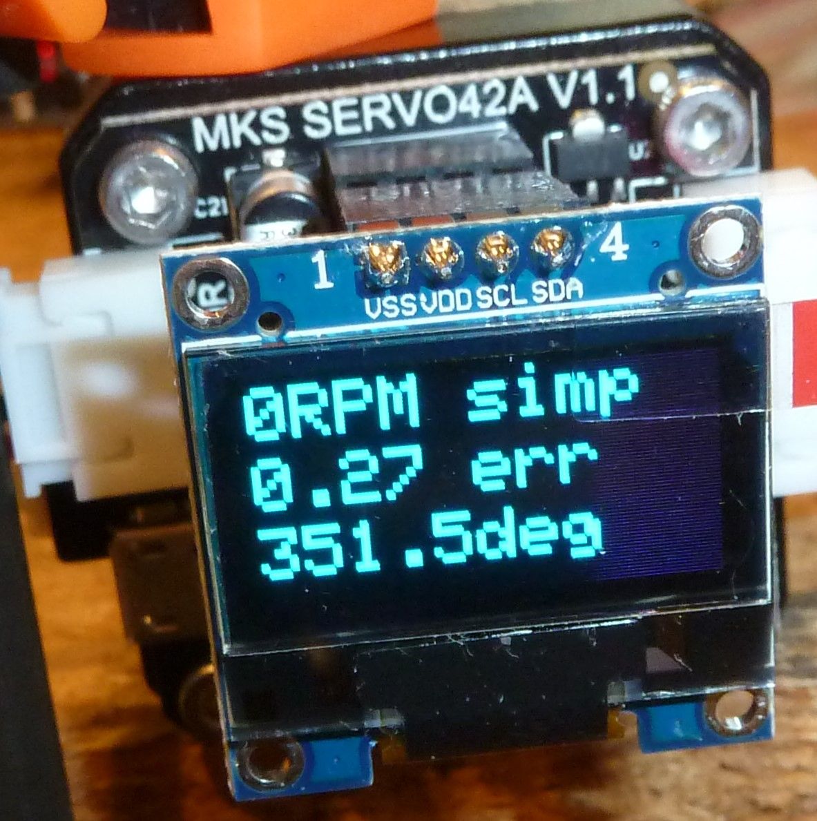
    It's up and running. In 256 step mode, it is barely even audible.

    However, given that, for a closed loop system the picture seems to represent a anomaly. Can you guess what it is? After jogging the motor around a bit, I stopped and let the stepper idle at what it thinks should be 351.5deg, based on the steps that I sent to it, but which the encoder measures as being 0.27 degree different than that. Well, we know that a full step would be 1.8 degrees, so if it is truly microstepping at 256 ,that means that each microstep should be able to advance the motor by 1.8/256=0.007 degree. Right? So, here's the rub: if the motor is idling, why hasn't it corrected, or at least significantly reduced, the 0.27 degree error? 0.007 degree is much less than 0.27 degree, so it should have adjusted the stepper's true position to be much closer to what its theoretical position should be. Yet, it isn't. Why not?

    Well, maybe it can't actually do 256 microsteps. Maybe it can do only 128. That would mean that it should be able to make each microstep be 0.14 degree. Right? But, if that were true, then being closed loop it again should have moved the stepper to bring it closer to what it should be. But it didn't.

    So, here's my theory: it's can't actually do 128 microsteps either. Maybe the most it can do is 64 microsteps. In that case, each microstep would be 0.28 degree. Right? But the error is 0.27 degree, which is less than 0.28 degree. Maybe that's where their algorithm gives up and stops. However, if it were me writing the code, I would have made it so that it moves one microstep closer to where it should be, even if that means overshooting by 0.01 degree. That's because being off by 0.01 degree is better than being off by 0.27 degree. But it didn't do that.

    However, if we assume that whoever wrote the code actually did the best job that could be done at closing the loop in this scenario, then the obvious conclusion is that this stepper driver can actually do at most 32 microstepping and nothing more. Why? Because in that case each microstep would be 0.56 degree, and so trying to close the loop by moving the stepper one microstep toward the position it ideally should have would mean overshooting by an amount greater than 0.27 degree, and so it's actually better to do nothing in this particular situation.

    But if that's the case, why advertise it to have more microstepping than what it's actually capable of?

    Anyhow, that's as far as I've gotten with it so far. I guess the next step will be to open up a terminal window to view its output over the usb connection. Perhaps that will shed more light on the mystery.

    Edit: Whooops. 1.8 degree divided by 32 is 0.056, not 0.56, so my calculations above are off. Well, I'm heading off to bed right now, so I'll look into that discrepancy tomorrow. Meanwhile, if anyone has thoughts on the 0.27 degree anomaly, feel free to post.

    That's it for today. Signing off. 😴 🛌


  • @NeverDie The UV laminator just gave me the craziest idea: Why don't we take a normal laminator, remove the heating coils and add a strip of UV leds to it??? The expected result: perfect pressing of the artwork to the board and curing at the same time, speed it travels through sets the hardening level. I can get rid of all those glass panels and stuff.
    I'm going out hunting for a cheap laminator 🙂


  • @executivul good luck.

    I noticed that I really have to hold the board and the plastic together, otherwise the rolls will pull the foil off the board.

    So that might make aligning the artwork a bit difficult. Perhaps some form of holder for the PCB could prevent the shifting.


  • Hero Member

    @executivul said in CNC PCB milling:

    @NeverDie The UV laminator just gave me the craziest idea: Why don't we take a normal laminator, remove the heating coils and add a strip of UV leds to it??? The expected result: perfect pressing of the artwork to the board and curing at the same time, speed it travels through sets the hardening level. I can get rid of all those glass panels and stuff.

    @executivul I like how you think. That's a great idea!


  • Hero Member

    @Joerideman said in CNC PCB milling:

    @executivul good luck.

    I noticed that I really have to hold the board and the plastic together, otherwise the rolls will pull the foil off the board.

    So that might make aligning the artwork a bit difficult. Perhaps some form of holder for the PCB could prevent the shifting.

    The margin on the MYOS looks pretty big toward the top and bottom. My guess is it's there, at least in part, for the reason you mentioned.

    Also, that cold laminator I posted earlier that you guys pooh-poo'hd had a feature that maybe your particular hot laminator lacks, which is adjustable pressure. You could potentially run it through more than once, and crank up the pressure with each pass. Probably some hot laminators have this type of feature.


  • Hero Member

    @NeverDie said in CNC PCB milling:

    Well, maybe it can't actually do 256 microsteps. Maybe it can do only 128. That would mean that it should be able to make each microstep be 0.14 degree. Right?

    Wrong. 0.014 degree.

    But following the rest of the chain of reasoning with the shifted decimal place, it becomes obvious that something is wrong with the closed loop algorithm, because it proves that not much microstepping granularity is required to correct for a 0.27 degree error.

    The shorter way to prove it is simply: 1.8/0.27=6.7. So, even an 8 microstepping division would be able to reduce the final error if the algorithm were to correct the stepper's final position, which it didn't do.

    I wouldn't yet rule-out user error though. Not yet sure what that would be, but I'll take another pass at it.

    Regardless, I already like it far more than the DRV8825 because it's not blowing up either itself or the GRBL arduino, and it appears to consume a lot less current while jogging.

    Because I have only these three controllers to work with, I earlier outfitted all 3 with oversized pure copper heatsinks and permanently secured them tight with artic-silver thermal epoxy:
    copper_heatsinks.JPG
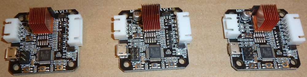
    Thinking about that now, I suppose that in doing so there's some risk that, because of the weight, a lot of vibration might eventually rip the entire stepper chip off the board. Meh, hopefully it's moot: I'm etching PCB's, not milling stainless steel. If I were doing that instead, I can see the advantage of not having the stepper driver directly attached to the stepper motor.


  • Hero Member

    I found this critique of the MKS servo42A by what sounds like my have been one of the developers of the original smart stepper:
    http://misfittech.net/blog/makerbase-mks-servo42/

    He obviously sounds rather bitter about MKS not making their firmware public. However, although I'm not 100% sure, it looks to me as though not long afterward MKS may have posted it to github here: https://github.com/makerbase-mks/MKS-SERVO42A/tree/master/Firmware/stepper_nano_zero

    TL;DR: MKS cut some corners when they cloned the servo42A, and so, although similar, in his view it's not as good as the original, which he is still selling for $50 plus add-ons plus shipping. i.e. more than 3x the price of the MKS version. Among other things, he says MKS removed an "error" pin and chose a less accurate magnetic encoder than what his design uses.


  • Hero Member

    Ugh. Confirmed: MKS Servo42a uses A1333LLETR-T, which has 12 bit resolution, instead of AS5047D that the mechaduino uses, which has 14 bit resolution. I'm very disappointed.

    This compares to uStepper, which uses AEAT8800-Q24, which is a 16 bit magnetic encoder, which according to uStepper gives a resolution of ~0.0055 degrees

    For the z-axis I want all the resolution I can get, so I'm going to order a uStepper and see how it compares on the bench. It's 3x the price of the MKS stepper but nominally has 16x the resolution.


  • Mod

    @NeverDie said in CNC PCB milling:

    nominally has 16x the resolution

    Why? Going from 12 to 14 bit on the on the encoder will only give 4x the resolution...


  • Hero Member

    @Yveaux said in CNC PCB milling:

    @NeverDie said in CNC PCB milling:

    nominally has 16x the resolution

    Why? Going from 12 to 14 bit on the on the encoder will only give 4x the resolution...

    You must have missed it. uSstepper has 16 bit resolution. So, 4 extra bits of resolution.


  • Mod

    @NeverDie ah, ok, nevermind. Too many part numbers and bit references in a single post for my peanut brain 😬


  • Hero Member

    @Yveaux said in CNC PCB milling:

    @NeverDie ah, ok, nevermind. Too many part numbers and bit references in a single post for my peanut brain 😬

    Don't feel bad. Unlike me, you still have your money! I had assumed that because the MKS SERVO42A appeared to be a rip-off of the mechaduino design that they had copied the BOM as well. Instead, they made it worse. If it hadn't found the rant I linked to above, it might have taken me a long-time to realize the difference.

    Edit: I just now ordered a uStepper S, which is the 16 bit version. Coming from Denmark with Danish postal shipping (the only option) it may take a couple of weeks to get here. Unless I'm mistaken, it is the highest resolution closed-loop stepper driver+encoder combination currently on the market (well, excluding whatever big ticket industrial solutions may exist). Is it overkill given the other sources of slop in my existing rig? Maybe. I would guess so, but right now I don't have a quantified grasp of just how good or bad the other system components are performing, so I can't really say with any certainty.

    Edit: I looked into the possiblity of desoldering the 12-bit encoder on the MKS servo42A and then soldering on the original 14 bit magnetic encoder in it place. Unfortunately, the pinout is different, so that's not a practical option. Looking back, it would have been better to build a mechaduino from scratch using the open source files and thereby completely remove slip-shod aliexpress profiteers from the equation. Lesson learned! It's much harder to rely even on reviews anymore, since many of those now seem to be infiltrated by the marketers. Even on amazon. These days it has become a serious obstacle to making an informed purchase decision.


  • Hero Member

    Does anyone here know how to invert (take the negative) of a gerber image? Because it's open source, I'd like to order some extra uStepperS boards (it would be much faster than ordering a fully populated board from Denmark), but they used Altium Designer, which inverts the ground plane:
    needToInverty.png
    If I were to submit this to a fab, it would come out wrong.

    In theory, if I were to change the layer to a "signal" layer instead of a "plane" layer, it would be correct. I tried that, but in this case doing that erases the contents of the layer, so that's no good as an after-the-fact solution.

    I tried looking for a gerber editor that could do this, but I only found one, and despite it promising "download now", all it did was collect my information and provided no download.

    Anyone? Bueller? Anyone?


  • Hero Member

    I figure full 14-bit resolution of absolute position will be enough, and that's what the AS5048A promises: https://www.mouser.com/datasheet/2/588/AS5048_DS000298_4-00-1100510.pdf That's 0.0219 of a degree resolution.

    As near as I can tell, the AS5047D that the mechaduino chose instead delivered much less than that. According to the datasheet it had " a maximum resolution of 2000 steps / 500 pulses per
    revolution." I'm not entirely sure what that means in this context, because in the paragraph just before that it says, "A standard 4-wire SPI serial interface allows a host microcontroller to read 14-bit absolute angle position data
    from the AS5047D," which makes it sound as thought 14 bit resolution should have been achievable, but apparently it wasn't. https://www.mouser.com/datasheet/2/588/AS5047D_DS000394_2-00-1513297.pdf

    In the case of the AS5048A, however, whatever ambiguity that clouded the AS5047D datasheet has been lifted, because according to https://ams.com/as5048a the AS5048A is capable of 16384 positions per revolution, and it doesn't discuss "steps" at all.

    Interestingly, this chip has been on the market for quite a while and so there are a number of github libraries for it. It is protected by a patent filed in 2005 in Europe and 2006 in the US (US Patent 7,095,228).


  • @NeverDie I use this steps, and I'm quite satisfied

    https://www.mischianti.org/2019/03/14/design-and-mill-pcb-easy-and-cheap-part-5/

    Nothing special, but works correctly..


  • It highly depends on the lead/ball screws, if the tolerances are in range of 0.01mm and backlash at about 0.1mm a 0.X deg of resolution at the steppers/servos doesn't matter since a normal lead screw is 4-8mm/turn.
    Even 200 full steps/rev (1.8 deg stepper and full steps) with 4mm/rev screw means 50 full steps/mm or 20 micron/step (0.02mm/step) linear resolution which is much better compared to the rest tolerances of the machine.
    On high precision rails, very tightly built machine it might make a difference, but for these cheap routers it doesn't.

    LE. @NeverDie 0.27 deg error translates to 0.003mm linear error (3 microns) assuming 4mm/rev screws are being used. Do you think you can notice/measure that? (4mm/360)*0.27=0.003 Even if using HUGE 16mm/rev ball screws translates to 0.012mm of error, unnoticeable.


  • @andrew Have you got your new 3020T yet? I intend to buy 3020 but there are a few variants in Aliexpress. Which site did you buy from? Can you share the link? Thank you for starting this thread.


  • Hero Member

    @executivul That's how I previously looked at it, but now I'm looking at it as: total error = sum of individual errors. Previously, for any particular fix I could talk myself out of it by an argument such as the one you articulated. However, even though the individual errors may be small, they may sum up to something bigger that is noticeable. So, this is the first of what I hope will be at least a few refinements, and the hope is that the sum of the refinements will make a difference even if not much is improved by any one of them.

    I'm not sure what to do about "following error" though other than to move more slowly. All machines have it to one degree or another. I think everyone who has closed-loop becomes aware of it very quickly because it suddenly becomes so easy to track. I suppose more powerful motors and faster acceleration would help, but ultimately I think maybe better motion planning and control influenced by closed-loop feedback is what's needed. However, I'm not sure if that technology even exists yet. Maybe somewhere in LinuxCNC or something like that? Ultimately, maybe what's needed is closed-loop DRO feedback. The hardware isn't cheap, and figuring out how to retrofit it on to an existing system looks to be challenging. Still, it might be worth it. High quality Industrial grade CNC machines all seem have it.

    And what about software backlash compensation? How well does that work? I'm thinking that with DRO monitoring that would be a lot easier to dial in. One thing helps another.


  • Hero Member

    I cured some uv solder mask using the roller method. As a result of that experience I'm going to change over to a UV light that doesn't have a bottom. That way I won't disturb the work by picking up the wet film stack and moving it into under the UV light to cure. Instead, without moving the wet film stack, I'll simply position the UV light over the stack and turn it on.

    I can now confirm that polypropylene does a very good job of not sticking to the solder mask.

    Thickness on my solder mask came out uneven, but maybe that will improve with further experience. I put a 1/4" piece of glass over the wet film stack before rolling it, so I'm not sure where the waviness in thickness came from, except maybe from me disturbing the stack while relocating it to be under the UV light.

    I found a 3 mil drawdown bar and a 4 mil drawdown bar, so after the new UV light source arrives I'll have a try at laying down the solder mask wet film using those.

    I'm actually getting two new UV light sources, as I'm not sure which I will prefer. One uses UV tubes (which it claims emits at 365nm) and which gets rave reviews on amazon from people who are using it to cure uv resins:
    https://www.amazon.com/gp/product/B012MEZP2E/ref=ppx_yo_dt_b_asin_title_o03_s00?ie=UTF8&psc=1
    The downside is that the uv tubes reportedly burn out after a while and need to be replaced.

    The other is just a larger UV LED nail dryer, like the one I tried last night, except that it has no bottom, as I discuss just above:
    https://www.amazon.com/gp/product/B07MC4CZS1/ref=ppx_yo_dt_b_asin_title_o02_s00?ie=UTF8&psc=1


  • @NeverDie

    Years ago I bought a face tanning device. They still sell these things second hand. And I expect like a lot of convenient but time consuming beauty devices, they are hardly used.

    Cost you 5-10 euros here in the Netherlands. You might have something similar.

    Anyway 30 seconds with this thing and it's cured.


  • Hero Member

    An idea discusssed on Hackaday is to remove the UV filter on a personal pocket projector and then use the projector to project a solder mask image directly onto the solder mask of a PCB. If it can be made to work, this seems fairly elegant to me.

    I hadn't realized that personal pocket projectors had become so affordable. You can buy a new 1080p pocket projector on ebay for as little as $30-$50.

    A different Hackaday project uses Kapton tape cut by computer to somehow make a one-off solder mask for prototyping prototyping purposes.. Whatever works!


  • @NeverDie I just read back around 2017.

    Have you ever managed to get Andrews result? He claimed 6mil back then.


  • Hero Member

    @Joerideman said in CNC PCB milling:

    @NeverDie I just read back around 2017.

    Have you ever managed to get Andrews result? He claimed 6mil back then.

    Not consistently. That's why I'm doing a new round of improvements now. Somehow it's always the last little bit that consumes the largest share of the effort.


  • @NeverDie my UV lamp is made from a UV led strip glued to a cardboard box, I just place the UV over the board not the board in the lamp.

    The so called 1080p cheap projectors are actually 640x480 real resolution, or even 320x240, they are able to accept a 1080p signal and scale it down so are falsely advertised as FullHD. That was the state of things a year ago when I last checked. Much better to get a sh brand projector instead.
    About resolution: FullHD 1920x1080 over a 150x100mm board gets you 10pixels/mm roughly, that is 0.1mm resolution, I don't know if that is good enough, also focusing at such a close range would require some lens hacking, from the factory they focus at 50cm at least and get you a 60-100cm diagonal size.


  • Hero Member

    @NeverDie said in CNC PCB milling:

    @NeverDie said in CNC PCB milling:

    You probably want to aim for a thickness above the copper of about 0.5mm

    Correction: I should have said 0.5 mils.

    That's according to altium: https://resources.altium.com/p/how-choose-correct-solder-mask-your-pcb#:~:text=The typical solder mask thickness,solder mask over your traces.

    However, I'm not sure if they're referring to wet film thickness or dry film thickness. I guess with uv cured paint it maybe would be the same either way?

    I found that certain brands of Kapton tape are advertised to be 0.5 mils thick: https://smile.amazon.com/gp/product/B00EP254UU/ref=ppx_yo_dt_b_asin_title_o00_s00?ie=UTF8&psc=1

    I've ordered some and will try using that to set the film thickness of the solder mask when I flatten it out between two very flat 1/2" thick panes of glass.


  • Hero Member

    For purposes of solder masking, I compared a number of black markers for drawing on PP sheeting to see which would be the blackest and most opaque. I compared: Inkzall, regular Sharpie, Sharpie Oil, and POSCA (a Japanese paint pen). By reputation I had thought the POSCA would win, but by far the blackest and most opaque of the bunch was the Sharpie Oil. It appeared to be genuinely opaque. The Inkzall and the regular sharpie were not opaque at all.


  • Hero Member

    Reporting back: After letting it dry overnight, I discovered that the Sharpie-Oil apparently shrinks and then flakes off of the PP film:
    p0.JPG

    Not sure if it behaves better with other films or not.

    However, before it dries, it performs great, as seen below.

    Here I am squishing solder mask between two thick sheets of glass:
    p1.JPG
    This technique seems to do a reasonably good job of producing a uniform thickness of the UV solder mask.

    Here I use a Sharpie Oil marker to print the word OIL and place it over the flattened solder mask before exposure to UV:
    p2.JPG

    I exposed it to UV for a full 99 seconds, which may have completely cured the non-masked solder-mask. Here is how it looks after I removed the "OIL" mask:
    p3.JPG

    Here is how it looks after peeling back the top layer of PP film:
    p4.JPG

    I then removed the uncured solder mask using IPA, after which I cured it some more under UV just to be sure:
    p5.JPG

    As a first attempt, not bad! Using a high opacity mask probably helped quite a bit.

    So, I guess now the question is: which inkjet ink/pigment or which laserjet toner has the highest opacity? For instance, there is this which claims to be: https://www.amazon.com/Ink-Dynasty-Resistant-Refillable-cartridge/dp/B00E3PAUXA
    or this:
    https://www.screenerschoice.com/index.php?route=product/product&product_id=157

    From the looks of it, the answer will be some kind of inkjet black pigment, which is consistent with the results I got from comparing ink pens vs paint pens above.


  • @NeverDie I saw an YouTube video screenprinting. That guy noticed that semi transparent sheets work better than transparent sheets. Ink holds better or something.

    I can actually try this one out. Because afteral. We want that 0.4mm pitch right?

    I just need to find something to put the paint on.


  • Thank you very much.


  • Hero Member

    @Joerideman said in CNC PCB milling:

    @NeverDie I saw an YouTube video screenprinting. That guy noticed that semi transparent sheets work better than transparent sheets. Ink holds better or something.

    I can actually try this one out. Because afteral. We want that 0.4mm pitch right?

    I just need to find something to put the paint on.

    Which thing are you planning to try? Sharpie-Oil on a semi-transparent sheet, or the uv resistant inkjet ink, or...?

    For enhanced laser printing I found this: https://ikonartstencil.com/toner-enhancement-spray/
    though I have no idea how well, or even if, it works.


  • Hero Member

    I received some Sharpie-Oil "Extra Fine" pens. Testing them, they have a 1mm line width, so they'd be no good for filling in features smaller than that. AFAIK, they have the smallest tips in the Sharpie-Oil series.

    I received the 16-bit closed-loop uStepper hardware from Denmark, so I'll be testing that sometime soon. I intend to use it on the z-axis, since accuracy on depth of cut is critical. If even this is still not enough, then I'll work harder to identify the source of the error and, if appropriate, consider stronger measures like low run-out collets, low-runout bits, ball-screws, tighter linear rails and/or tracking absolute position with a DRO and/or possibly a different spindle.


  • @NeverDie inkjet printing on semi transparent sheets.


  • Hero Member

    I've played around with the Ustepper-S now, and as near as I can tell, it is working correctly in closed-loop mode without issue. After the execution of each command, it shows error of 0.00, and it maintains closed loop operation to maintain its position even after the execution of the command, as it should. In my testing, Servo42A fails to do that, as well as having other problems, including lack of response to posted github issues.

    Ustepper-S incorporates PID, so it should be able to do rapids and yet stop exactly where it should. Again, my initial impression is that seems to be the case.

    I'm ordering UStepper-S for the x and y axis as well, which unfortunately will again take weeks to receive. However, I expect this will be the last stepper driver upgrade that I will ever need to do. If I later decide to upgrade to NEMA-23, the same UStepper-S can be used to drive it and only a different bracket would be needed to position it on the back of the NEMA-23.


  • Hero Member

    I found a good "once and done" lubricant for my CNC called Krytox. It's made by Dupont, is non-toxic, never dries out, and is non-reactive with just about everything. It is more or less liquid teflon (PTFE). It comes in a wide spectrum of different viscosities. I'm using GPL105, but I think for a CNC one could argue for using a version that's a least slightly more viscous (i.e. GPL106 or higher).

    There also exists grease versions of Krytox, so perhaps (?) that would be even better. In general, for any given lubricant, how does one decide what the right viscosity is to use?


  • @mlei30 This was my choice:
    https://www.ebay.com/itm/CNC-Router-3020T-3-AXIS-USB-Graviermaschine-GraviergeräT-FräSmaschine/313030564524
    It already arrived and I started to play with it.
    I decided not use its Chinese controller software or Mach3 with parallel port connection, so it needs some upgrade before I can make the first tests with it.
    There are tons of upgrade options to make it work with open source stuff. I almost ordered a TinyGv2 controller, but it turned out, that that CNC can be GRBL controlled over the parallel port. In such case,
    original stepper and spindle drivers can be used as well.

    The problem is, that the research I found behind this was misleading and it contains inaccurate / improper details (or at least not exactly applicable to my HW version), so I had to re-execute the reverse engineering.

    I'm about to finish it. At the moment I can control everything on the CNC from GRBL. Now I need to calibrate it and make the solution "solid/proper". I have hard time finding free time for this, but I hope that first test runs will be done soon.

    I'll be back with the results soon (and I'm also planning to write a blogpost on the details later).


  • Hero Member

    @andrew Looks as though your new nema steppers either have encoders or else those are knobs for manually jogging. Aside from that, it looks generally stiffer due to all metal with no plastic.


  • @andrew

    • Does it use ball screws or trapezoidal ones?
    • how stiff it is in X an Y directions?
      (on my machine slight push on spindle, yields ~0.2mm of flex, and heavier one around 0.5mm, which is roughly precision I get when cutting plastic. For PCB routing error seems to stay within 0.2mm boundary)
    • how big is backlash
    • screw (movement) linearity in X,Y planes


  • @NeverDie it is a knob for manual positioning. the whole assembly and machine is very massive and stable, all metal parts do matter a lot.


  • @niallain it is 3020T which uses trapezoidal screws. "Z" uses ball screws.
    you can check the "official" technical details on the item's specification (scroll down to the description then click on the "specification"):

    ...
    Driving units X axis: 1204 trapezoidal screws
    Driving units Y axis: 1204 trapezoidal screws
    Driving units Z axis: 1204 trapezoidal screws
    ...
    Repeat accuracy: 0.05mm
    ...
    Spindle precision: radial beat acuities 0.03 mm
    ...

    Note that none of these parameters above are confirmed. To be honest I don't have the right measurement tools for that, but the fine trace PCB samples will prove it, or not 🙂


  • @andrew

    @andrew said in CNC PCB milling:

    @niallain it is 3020T which uses trapezoidal screws. "Z" uses ball screws.
    you can check the "official" technical details on the item's specification (scroll down to the description then click on the "specification"):

    declared specs for mine were in the same ballpark as your's 3020T, modulo 8mm trapezoidal screw. But in reality that wasn't true at all, in my case cuplrit of the biggest error is the flex from the way screw nuts are attached to carriage, and the second/third are nonlinear screws (+-0.060mm) and backlash.

    I'm ordered a 1204 ball screw kit for Y axis, to test how much it would reduce error.

    PS:
    As for testing, I just used regular digital calliper with 0.01mm resolution.


  • Hero Member

    @niallain said in CNC PCB milling:

    in my case cuplrit of the biggest error is the flex from the way screw nuts are attached to carriage, and the second/third are nonlinear screws (+-0.060mm) and backlash.

    I'm curious to know how is it that you're measuring those things? I'd like to quantify as many sources of error as possible, but I'm not sure how to go about it.


  • @NeverDie How about a dial gauge in a magnetic mount attached to the spindle and measuring against x/y/z frame points, and a simple gcode like g0x100 g0x0 a hundred times? At least that's how I did it to check for lost steps.


  • @NeverDie
    I shoot a short clip to demo following measurements

    • backlash :
    • flex: for example I used dial gauge, since my Y screw and table are currently dismantled, so I can't show how it's done with calliper on the table
    • non-linearity is measured only on 1mm, with calliper or glass scale it would be possible to measure whole screw. (linuxcnc can use glass scale to map screw and then compensate, but I still don't have all components for it yet)

  • Hero Member

    @niallain said in CNC PCB milling:

    • non-linearity is measured only on 1mm, with calliper or glass scale it would be possible to measure whole screw. (linuxcnc can use glass scale to map screw and then compensate, but I still don't have all components for it yet)

    That's quite an interesting result! I would not have imagined it would be so bad. What exactly is happening that causes this? Is the screw being wound up almost like a spring and some kind of stiction is causing the carriage to jump about like that? Is the anti-backlash nut causing it? Or is the stepper in fact not advancing as much as it should be due to no closed-loop feedback? What's the cause? How repeatable is it? i.e. does it jump about to the same amount in the same places each time it's cycled through the test, or does it vary each time the test is repeated?

    It's a great advertisement for DRO's.


  • Hero Member

    Reporting back: Regarding Sharpie-Oil pens, I found that it doesn't chip-off and disintegrate, even after letting it dry for a few days, if I write it onto inkjet transparency material instead of polypropylene:
    P1100137 (2).JPG

    Because it's so opaque, especially when compared to other black pens, it's the best pen I've found. The linewidth of the "Sharpie-Oil Extra Fine" pen is about 1mm, though, so that precludes using it in a plotter if ultra fine detail is required.


  • @NeverDie however.... The material sticks a bit to the paint.


  • Hero Member

    @Joerideman said in CNC PCB milling:

    @NeverDie however.... The material sticks a bit to the paint.

    ??? Which thing are you referring to?

    Right, so I still use the polyproylene against the solder mask, but I can layer this inkjet tranparency on top of that. It's an extra layer, but it's kept separate from the solder mask by the polypropylene layer underneath it. Is that what you mean?


Log in to reply
 

Suggested Topics

  • 4
  • 2
  • 5
  • 3
  • 1
  • 9

0
Online

11.2k
Users

11.1k
Topics

112.5k
Posts