💬 The Harvester: ultimate power supply for the Raybeacon DK
-
@Mishka said in 💬 The Harvester: ultimate power supply for the Raybeacon DK:
I'm still not used to the numbers and feel that if we take a couple more steps, we will go to the quantum level
LOL. In that case, strap yourself in Dorothy, because Kansas is about to go bye-bye: here's a voltage detector which claims to have a quiescent current of less than 6 pico-amps!
! https://www.bristol.ac.uk/media-library/sites/engineering/research/eem-group/zero-standby/UB20M_Datasheet_Rev.1.5.pdf
The only thing which appears to tarnish that claim is that it has a leakage current of 100 pico-amps. Even so, though, I'm not aware of anything else that even comes close to that. If it does what it claims to do, then I'm imagining we could harvest energy from even a very dark environment and yet still be net positive on harvested energy (without the control hardware consuming all of it and then some). :-)Unfortunately, their UB20X chip doesn't seem to be stocked anywhere. I sent an email to the company yesterday to inquire about how to buy it, but so far I haven't heard anything back yet. I hope they're still in business.
-
@NeverDie Well :-)
What can I say? Only that the PDF is here. They seem achieved this ridiculous leakage with careful transistor selection. Very nice!
@Mishka Thank you very much for that link. Gosh, it sure would have been awesome to have such an ultra low power wake-on radio such as that described there. Unfortunately, I'm still getting no reply to even my second email attempt at contacting the company. Maybe they'll reply later, but for now I'm going to assume they are closed for business during the Caronavirus attack.
Fortunately, Figure 5 in the paper you linked shows an equivalent transistor layout for the voltage detector. It lacks a BOM with part numbers, but I'll nonetheless take a quick run at trying to simulate it in LTSpice--maybe I'll get lucky. If you were in my shoes, exactly which simulated transistors/mosfets would you be trying?
As for alternatives to the UB20M, the nearest I could find is this:
https://www.ablic.com/en/doc/datasheet/photo_ic/S5470_E.pdf
which, admittedly, isn't as nice because it is an ultra low current detector rather than a low voltage detector. Its quiescent current is higher than the UB20m, but it appears to be still quite low in absolute terms. What the S5470 does have that the UB20M lacks though is that the s5470 is well stocked at Digikey and similar places. :)Have you run across any other parts that might fit the UB20M role?
Edit: I put Figure 5 into LTSpice. I could get it to generate the ~100mv reference voltage, but it doesn't appear to switch anything nor "detect" and then switch anything either. So, maybe there is more to the circuit that what they are showing. Given the circumstances of not being able to acquire their UB20M, it's a bit of a let down. :(
-
The last option I can think of would be to try these special mosfets from Advanced Linear Devices:
https://www.aldinc.com/pdf/ALD110802.pdf
The gate leakage and drain source leakage combined is typically just 13pa. They can switch at around 0.2v, which, I suppose (?), could be viewed as a kind of voltage detector. Maybe in that sense, then, it even outperforms Bristol's UB20M? Also, unlike the UB20M, they seem to be relatively available through digikey, mouser, etc. -
@Mishka Thank you very much for that link. Gosh, it sure would have been awesome to have such an ultra low power wake-on radio such as that described there. Unfortunately, I'm still getting no reply to even my second email attempt at contacting the company. Maybe they'll reply later, but for now I'm going to assume they are closed for business during the Caronavirus attack.
Fortunately, Figure 5 in the paper you linked shows an equivalent transistor layout for the voltage detector. It lacks a BOM with part numbers, but I'll nonetheless take a quick run at trying to simulate it in LTSpice--maybe I'll get lucky. If you were in my shoes, exactly which simulated transistors/mosfets would you be trying?
As for alternatives to the UB20M, the nearest I could find is this:
https://www.ablic.com/en/doc/datasheet/photo_ic/S5470_E.pdf
which, admittedly, isn't as nice because it is an ultra low current detector rather than a low voltage detector. Its quiescent current is higher than the UB20m, but it appears to be still quite low in absolute terms. What the S5470 does have that the UB20M lacks though is that the s5470 is well stocked at Digikey and similar places. :)Have you run across any other parts that might fit the UB20M role?
Edit: I put Figure 5 into LTSpice. I could get it to generate the ~100mv reference voltage, but it doesn't appear to switch anything nor "detect" and then switch anything either. So, maybe there is more to the circuit that what they are showing. Given the circumstances of not being able to acquire their UB20M, it's a bit of a let down. :(
@NeverDie said in 💬 The Harvester: ultimate power supply for the Raybeacon DK:
Fortunately, Figure 5 in the paper you linked shows an equivalent transistor layout for the voltage detector. It lacks a BOM with part numbers, but I'll nonetheless take a quick run at trying to simulate it in LTSpice--maybe I'll get lucky. If you were in my shoes, exactly which simulated transistors/mosfets would you be trying?
That's true. The components selection is the hard part. I din't find anything, but the MOSFET arrays by ALD, and I see you've found them already.
It seems the most of discrete elements are tied to nanoamps and only few are diving to picoamps area. For example, the Nexperia settled it to 25 nA, as well as the TI does. But for some selected integrated circuits there are the picoamps, and some opamps may draw only femtoamps which is impressive. There is also the nice article on possible design issues - quite surprising - when building such a uber-low-power circuit - https://www.edn.com/design-femtoampere-circuits-with-low-leakage-part-one/
As for alternatives to the UB20M, the nearest I could find is this:
https://www.ablic.com/en/doc/datasheet/photo_ic/S5470_E.pdf
...
The last option I can think of would be to try these special mosfets from Advanced Linear Devices:
https://www.aldinc.com/pdf/ALD110802.pdfYeah, that's it. And the cool part is that the ALD offers 2V*200nA=400nW energy harvesters which work very similar to those we're trying to design here - http://www.aldinc.com/pdf/EH300.pdf
Unfortunately, still not sufficient to run your a-Si 80nA solar panel.
Edit: I put Figure 5 into LTSpice. I could get it to generate the ~100mv reference voltage, but it doesn't appear to switch anything nor "detect" and then switch anything either. So, maybe there is more to the circuit that what they are showing. Given the circumstances of not being able to acquire their UB20M, it's a bit of a let down. :(
It has to switch the VOUT on as soon as the VINL will be high enough to close the MN5 and pull down the VREF thus resetting the triggers and causing them to produce the VOUT.
I've put it into KiCad and immediately failed with component selection. In addition to issues with the search of a low-current MOSFETs, the ngspice has incomplete support for the modern PSPICE models. And create own models is a cumbersome task :-(
After trial and errors I've ended up switching to ngspice internal models. After some trivial tuning the circuit started to work. I've just added input (storage) capacitor and have attached a simple load (switched with an additional N-MOS) to get the simple harvester work.
On VinL≥2V input capacitor is discharged to load R2 until VinL will drop below 1V. Both voltages are configured via MOSFET gate thresholds.
For details please take a look to the eeschema file - https://drive.google.com/file/d/1O8aVj7ZzjG1TNdTJOce4i2P65X-aRLgB/view?usp=sharing.
Voltages:
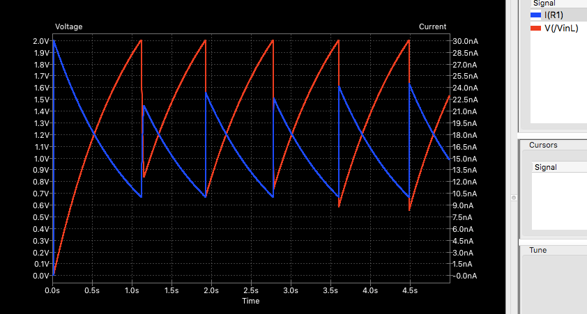
Input current I (via R1) in dependency of input voltage. I(R1) = 3V/100M = 33nA to simulate the a-Si cell.
I don't know how much current the circuit will draw in real life, but taking in account low voltage source (please note, datasheets mention 25nA as upper threshold) perhaps there are some chances to fit into the a-Si cell current budged.
-
@Mishka Thank you very much for that link. Gosh, it sure would have been awesome to have such an ultra low power wake-on radio such as that described there. Unfortunately, I'm still getting no reply to even my second email attempt at contacting the company. Maybe they'll reply later, but for now I'm going to assume they are closed for business during the Caronavirus attack.
Fortunately, Figure 5 in the paper you linked shows an equivalent transistor layout for the voltage detector. It lacks a BOM with part numbers, but I'll nonetheless take a quick run at trying to simulate it in LTSpice--maybe I'll get lucky. If you were in my shoes, exactly which simulated transistors/mosfets would you be trying?
As for alternatives to the UB20M, the nearest I could find is this:
https://www.ablic.com/en/doc/datasheet/photo_ic/S5470_E.pdf
which, admittedly, isn't as nice because it is an ultra low current detector rather than a low voltage detector. Its quiescent current is higher than the UB20m, but it appears to be still quite low in absolute terms. What the S5470 does have that the UB20M lacks though is that the s5470 is well stocked at Digikey and similar places. :)Have you run across any other parts that might fit the UB20M role?
Edit: I put Figure 5 into LTSpice. I could get it to generate the ~100mv reference voltage, but it doesn't appear to switch anything nor "detect" and then switch anything either. So, maybe there is more to the circuit that what they are showing. Given the circumstances of not being able to acquire their UB20M, it's a bit of a let down. :(
@NeverDie said in 💬 The Harvester: ultimate power supply for the Raybeacon DK:
Have you run across any other parts that might fit the UB20M role?
The UB20M is hard to beat. But there's another sub-nanoamp option: https://www.vishay.com/docs/66597/sip32431.pdf
-
@NeverDie said in 💬 The Harvester: ultimate power supply for the Raybeacon DK:
Have you run across any other parts that might fit the UB20M role?
The UB20M is hard to beat. But there's another sub-nanoamp option: https://www.vishay.com/docs/66597/sip32431.pdf
@Mishka said in 💬 The Harvester: ultimate power supply for the Raybeacon DK:
@NeverDie said in 💬 The Harvester: ultimate power supply for the Raybeacon DK:
Have you run across any other parts that might fit the UB20M role?
...But there's another sub-nanoamp option: https://www.vishay.com/docs/66597/sip32431.pdf
How would the vishay fit into it? Are you thinking you would switch it on-off using an ALD mosfet, or ...?
-
@NeverDie said in 💬 The Harvester: ultimate power supply for the Raybeacon DK:
Fortunately, Figure 5 in the paper you linked shows an equivalent transistor layout for the voltage detector. It lacks a BOM with part numbers, but I'll nonetheless take a quick run at trying to simulate it in LTSpice--maybe I'll get lucky. If you were in my shoes, exactly which simulated transistors/mosfets would you be trying?
That's true. The components selection is the hard part. I din't find anything, but the MOSFET arrays by ALD, and I see you've found them already.
It seems the most of discrete elements are tied to nanoamps and only few are diving to picoamps area. For example, the Nexperia settled it to 25 nA, as well as the TI does. But for some selected integrated circuits there are the picoamps, and some opamps may draw only femtoamps which is impressive. There is also the nice article on possible design issues - quite surprising - when building such a uber-low-power circuit - https://www.edn.com/design-femtoampere-circuits-with-low-leakage-part-one/
As for alternatives to the UB20M, the nearest I could find is this:
https://www.ablic.com/en/doc/datasheet/photo_ic/S5470_E.pdf
...
The last option I can think of would be to try these special mosfets from Advanced Linear Devices:
https://www.aldinc.com/pdf/ALD110802.pdfYeah, that's it. And the cool part is that the ALD offers 2V*200nA=400nW energy harvesters which work very similar to those we're trying to design here - http://www.aldinc.com/pdf/EH300.pdf
Unfortunately, still not sufficient to run your a-Si 80nA solar panel.
Edit: I put Figure 5 into LTSpice. I could get it to generate the ~100mv reference voltage, but it doesn't appear to switch anything nor "detect" and then switch anything either. So, maybe there is more to the circuit that what they are showing. Given the circumstances of not being able to acquire their UB20M, it's a bit of a let down. :(
It has to switch the VOUT on as soon as the VINL will be high enough to close the MN5 and pull down the VREF thus resetting the triggers and causing them to produce the VOUT.
I've put it into KiCad and immediately failed with component selection. In addition to issues with the search of a low-current MOSFETs, the ngspice has incomplete support for the modern PSPICE models. And create own models is a cumbersome task :-(
After trial and errors I've ended up switching to ngspice internal models. After some trivial tuning the circuit started to work. I've just added input (storage) capacitor and have attached a simple load (switched with an additional N-MOS) to get the simple harvester work.
On VinL≥2V input capacitor is discharged to load R2 until VinL will drop below 1V. Both voltages are configured via MOSFET gate thresholds.
For details please take a look to the eeschema file - https://drive.google.com/file/d/1O8aVj7ZzjG1TNdTJOce4i2P65X-aRLgB/view?usp=sharing.
Voltages:
Input current I (via R1) in dependency of input voltage. I(R1) = 3V/100M = 33nA to simulate the a-Si cell.
I don't know how much current the circuit will draw in real life, but taking in account low voltage source (please note, datasheets mention 25nA as upper threshold) perhaps there are some chances to fit into the a-Si cell current budged.
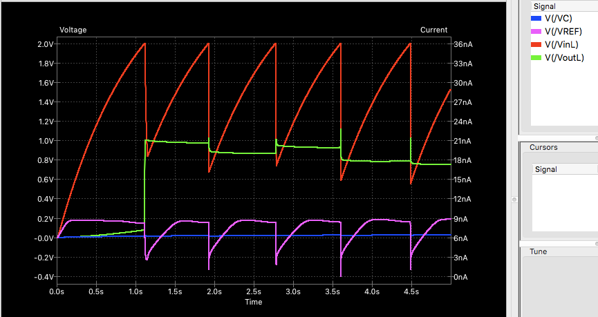
@Mishka Nice work getting it to switch. If I'm reading your graphs right, though, it look as though we're back to the land of 10+ nanoamps as opposed to the ~106 picoamps or so of the UB20M voltage detector, even though you're using the same transistor circuit as they are?
-
@Mishka Nice work getting it to switch. If I'm reading your graphs right, though, it look as though we're back to the land of 10+ nanoamps as opposed to the ~106 picoamps or so of the UB20M voltage detector, even though you're using the same transistor circuit as they are?
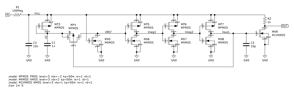
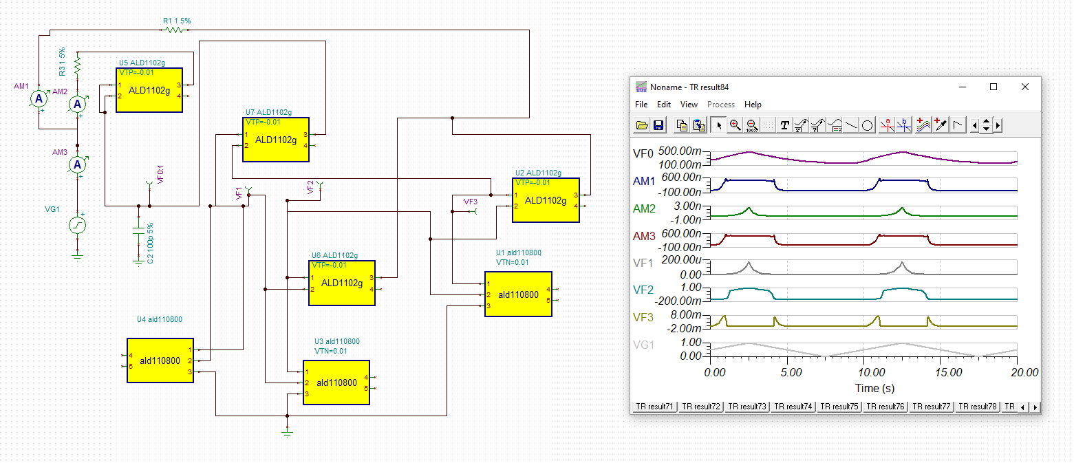
@NeverDie I've finally managed to make a readable image of the circuit. For our convenience, here it is:
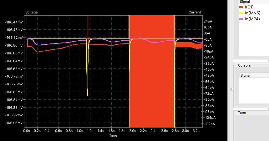
The circuit self consumption is comprised of MOSFETs leakage current, and current required to charge the C1 capacitor. Regarding C1 the startup current may be arbitrary low, but sufficient to charge it eventually. After that it won't require too much to sustain the circuit. For this particular ngspce model (where MOSFETs leakage is really low) those are picoamps indeed:
Those 30nA you've mentioned in my previous post are due to charging the C2 storage capacitor and is actually limited by R1=100MOhm resistor installed solely to emulate the weak a-Si panel. I.e. for one gigohm resistor it will not go higher than 3nA.
Of course, the model itself is far from being optimal and could be improved.
-
@Mishka said in 💬 The Harvester: ultimate power supply for the Raybeacon DK:
@NeverDie said in 💬 The Harvester: ultimate power supply for the Raybeacon DK:
Have you run across any other parts that might fit the UB20M role?
...But there's another sub-nanoamp option: https://www.vishay.com/docs/66597/sip32431.pdf
How would the vishay fit into it? Are you thinking you would switch it on-off using an ALD mosfet, or ...?
@NeverDie said in 💬 The Harvester: ultimate power supply for the Raybeacon DK:
@Mishka said in 💬 The Harvester: ultimate power supply for the Raybeacon DK:
@NeverDie said in 💬 The Harvester: ultimate power supply for the Raybeacon DK:
Have you run across any other parts that might fit the UB20M role?
...But there's another sub-nanoamp option: https://www.vishay.com/docs/66597/sip32431.pdf
How would the vishay fit into it? Are you thinking you would switch it on-off using an ALD mosfet, or ...?
I have no idea. Bipolar based opamps have similar characteristics, as well as the UB20M which seems build using FETs only.
:man-shrugging: -
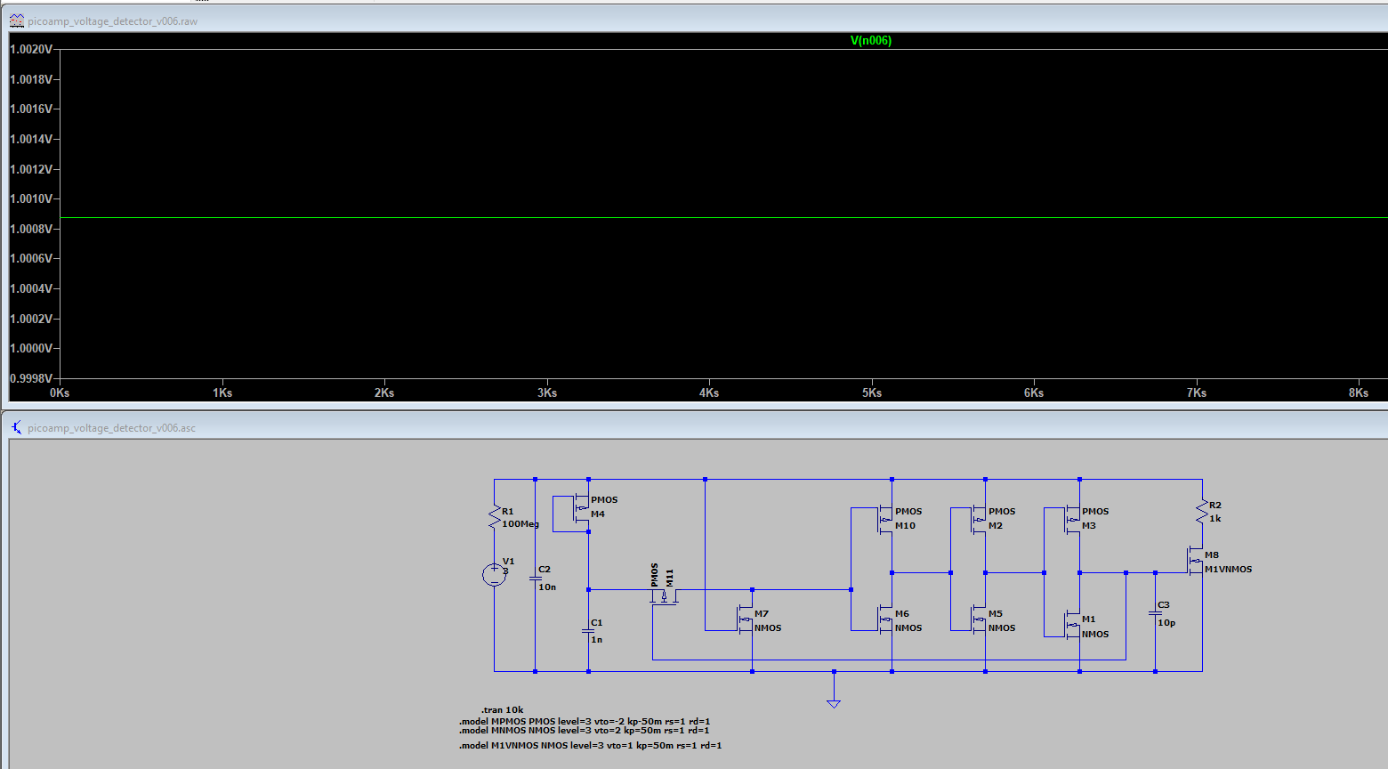
@NeverDie I've finally managed to make a readable image of the circuit. For our convenience, here it is:
The circuit self consumption is comprised of MOSFETs leakage current, and current required to charge the C1 capacitor. Regarding C1 the startup current may be arbitrary low, but sufficient to charge it eventually. After that it won't require too much to sustain the circuit. For this particular ngspce model (where MOSFETs leakage is really low) those are picoamps indeed:
Those 30nA you've mentioned in my previous post are due to charging the C2 storage capacitor and is actually limited by R1=100MOhm resistor installed solely to emulate the weak a-Si panel. I.e. for one gigohm resistor it will not go higher than 3nA.
Of course, the model itself is far from being optimal and could be improved.
@Mishka Fantastic!

I tried replicating it in LTSpice, but no joy as of yet using just the generic LTSpice parts. The magic must be in those ".model" statements, which I haven't yet entered.
What value are you using for your input voltage? It seems that a lot of it is getting dropped across the 100meg resistor, leaving not much left over for most of the circuit.
-
@NeverDie I've finally managed to make a readable image of the circuit. For our convenience, here it is:
The circuit self consumption is comprised of MOSFETs leakage current, and current required to charge the C1 capacitor. Regarding C1 the startup current may be arbitrary low, but sufficient to charge it eventually. After that it won't require too much to sustain the circuit. For this particular ngspce model (where MOSFETs leakage is really low) those are picoamps indeed:
Those 30nA you've mentioned in my previous post are due to charging the C2 storage capacitor and is actually limited by R1=100MOhm resistor installed solely to emulate the weak a-Si panel. I.e. for one gigohm resistor it will not go higher than 3nA.
Of course, the model itself is far from being optimal and could be improved.
-
@Mishka Fantastic!
I tried replicating it in LTSpice, but no joy as of yet using just the generic LTSpice parts. The magic must be in those ".model" statements, which I haven't yet entered.
What value are you using for your input voltage? It seems that a lot of it is getting dropped across the 100meg resistor, leaving not much left over for most of the circuit.
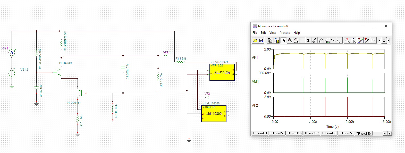
@NeverDie Oh, right. For the voltage source there is the 3V pulse defined as follows:
PULSE (0 3 20m 1u 1u 60 0)Reads like "start pulse from 0V to 3V, after 20ms timeout, 1us raise time, 1us down, keep it on for 60 seconds". This helped to examine how the circuit starts. But the circuit has to start with flat 3V input anyway.
All MOSFETs are defined with MOS level 3 model, zero-bias threshold (
vto) set to ±2 V, transconductance (kp) to 50 mA/V^2 to minimally reproduce a real transistor. Both drain and source has 1 Ohm resistance. Please note, the controlled NFET has lower voltage threshold at 1 V - this defines lowest VinL voltage. The rest of parameters can be derived from the ngspice manual, section 11.2.I expect that the ngspice and the LTSPICE may have different directives to setup the circuit :-(
Also, you may want to drop the C3, M8 and R2 thus leaving the circuit very similar to that one in the paper. The R1 still be used to limit input current, and the C2 will help to model raising voltage.
Also, does the
.tran 10kmeans 10k milliseconds? -
@NeverDie Oh, right. For the voltage source there is the 3V pulse defined as follows:
PULSE (0 3 20m 1u 1u 60 0)Reads like "start pulse from 0V to 3V, after 20ms timeout, 1us raise time, 1us down, keep it on for 60 seconds". This helped to examine how the circuit starts. But the circuit has to start with flat 3V input anyway.
All MOSFETs are defined with MOS level 3 model, zero-bias threshold (
vto) set to ±2 V, transconductance (kp) to 50 mA/V^2 to minimally reproduce a real transistor. Both drain and source has 1 Ohm resistance. Please note, the controlled NFET has lower voltage threshold at 1 V - this defines lowest VinL voltage. The rest of parameters can be derived from the ngspice manual, section 11.2.I expect that the ngspice and the LTSPICE may have different directives to setup the circuit :-(
Also, you may want to drop the C3, M8 and R2 thus leaving the circuit very similar to that one in the paper. The R1 still be used to limit input current, and the C2 will help to model raising voltage.
Also, does the
.tran 10kmeans 10k milliseconds?@Mishka said in 💬 The Harvester: ultimate power supply for the Raybeacon DK:
Also, does the .tran 10k means 10k milliseconds?
Actually 10,000 seconds. :astonished: That was just me throwing in a high enough number such that if there were ever to be observed an effect, I figure it would have shown up within 10,000 seconds. :blush:
I was playing around with an alternative to the original model, the better to understand how the original model worked, and I came up with something not as great, but maybe (someday, somewhere) it might be useful anyway if used as a trigger for one of the the ALD 20mv mosfets:
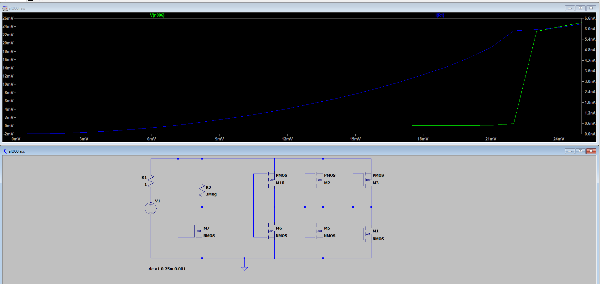
This is a voltage sweep simulation to show what happens at different input voltages. As you can see from the chart, the voltage on the output (the green line) stays pretty close to 0v up until it reaches around 22mv, at which point it it jumps up about 22mv in value. At that time about 6na of current is being conducted through R1 (the blue line in the graph), and so that is the total amount of current being consumed by the circuit.20mv is the minimum that the LTC3108 can startup and function at, so that is why I'm focused at such a low value.
It's quite an easily adjustable voltage "detector": using smaller values for R2 leads to higher trigger voltages, as well as higher voltages on the output. Of course, they also lead to higher currents, so maybe not so relevant to the matter at hand. However, if you ever need a voltage trigger that you can set to any value in some other context where current draw is not such a pressing concern, this might be an option.
Also, about 2/3 the current is being consumed by R2. If there were some other way to get a similar effect, but utilizing even less current, then that would be an improvement. Perhaps that's what the Bristol circuit manages to do. Perhaps choking off the current by using a high value for R1 (as in Mishka's simulation) and using a semiconductor of some kind in place of R2 would do the business.
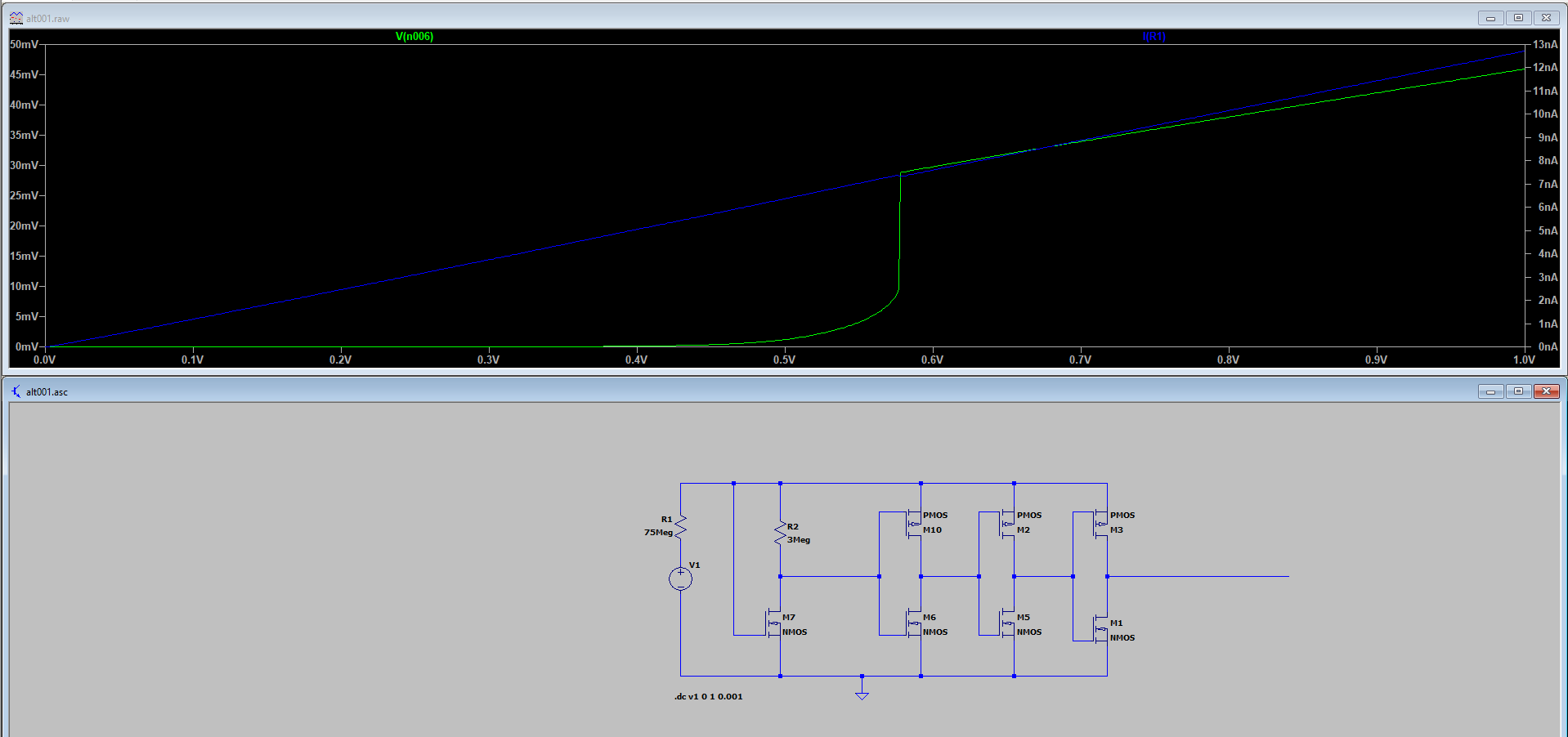
Edit: And just now noticing that by increasing the value of R1, the threshold for the detection voltage can be raised while keeping the current consumed in the single nanoamp digits:
In this case, with the higher threshhold, it might well be a useful complement to a 20mv ALD mosfet.
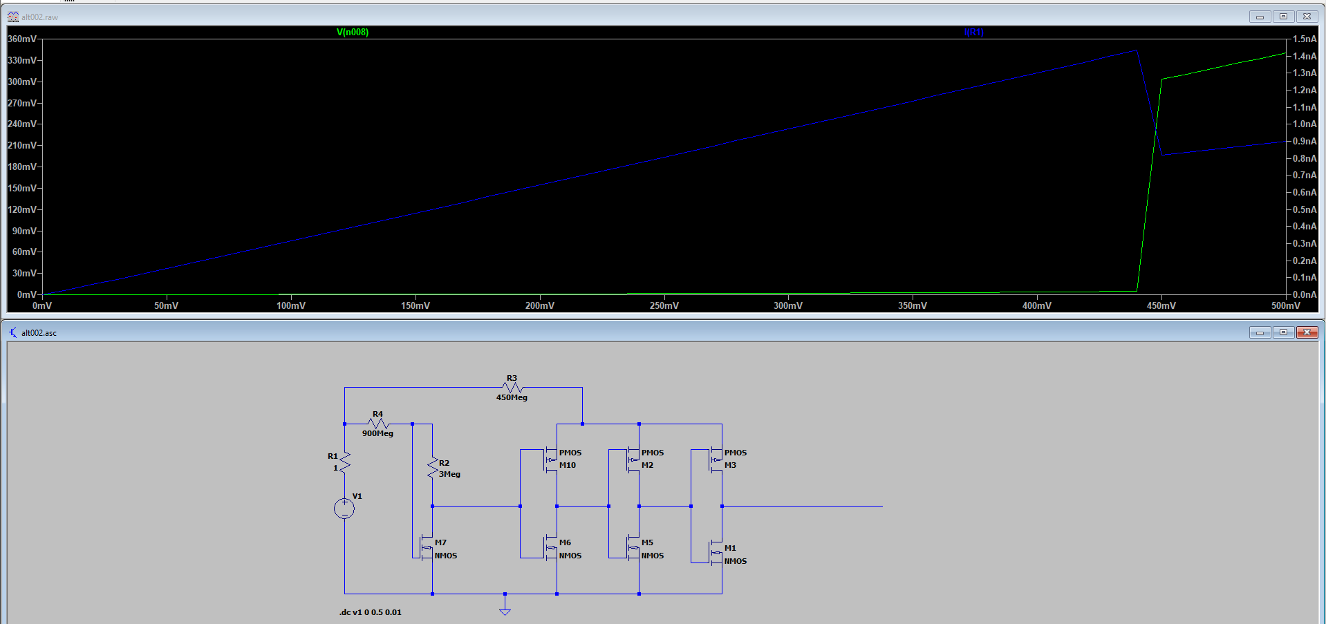
Edit2: Breaking out the resistance still further yields even more useful results: a larger transition voltage and even fewer nanoamperes.
These are just a few random attempts. A more methodical push would probably yield something better. I suppose trying it next with specific simulated components rather than whatever the simulator's generic components are would better inform whether a real world circuit could be built. -
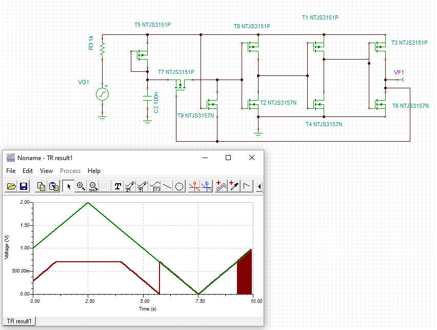
Answering my own question, I designed a circuit using "real" mosfets from the generic LTSpice library and got a nice snap transition on a "voltage detector", all while drawing less than 300picoamps:
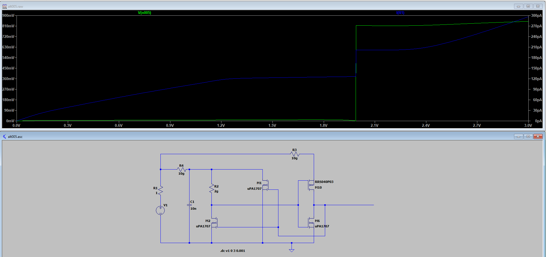
So, that's a simulated proof of concept. Now I just need to pull the trigger voltage down to a lower number, and I suspect that may involve using mosfets that aren't in the generic LTSpice catalog.Edit1: Ignore this particular circuit diagram. It turns out to be reducible to a much simpler circuit that draws even less current. I'm leaving it posted as a reference point for my own project tracking, but if not for that I would delete it.
Edit2: Lately LTSpice has, more often than not, failed to converge now that I have it simulating "real" mosfets. As a result I've started to look into TI's Tina circuit simulator, which AFAIK is also built on a SPICE platform. Although it's too soon to draw completely fair apples-to-apples comparisons, my initial impression is that TI Tina is much, much faster than LTSpice and also much better at converging. I'll update if that opinion changes.
Edit3: I've upgraded to using NTJS3151P and NTJS3157N as the simulation mosfets because they have lower threshold voltages and mouser has SPICE models for them that are free to download. I'm not yet endorsing them though, because it's just too early to say. They are just my first attempt, and there may be (probably are) better choices to be found. I'm finding it quite easy to import SPICE component models into TINA TI. I notice that some manufacturers, like Diodes Inc., actually rank their SPICE models as to how realistic they are.
@Mishka Which mosfets are you simulating? Head's up: I'd encourage you to find some real world simulated mosfets (you'll have to eventually anyway), because I'm found that, at least in LTSpice, the generic mosfets behave much, much differently than the apparently real-world simulated mosfets. Not sure why that would be so, but maybe their idealized nature are a little too idealized to be realistic in these types of circuits.
TINA TI lacks the convenience of a voltage sweep like LTSpice has, so I'm using a very low frequency triangle wave to approximate it.
Edit4: I'm starting to make progress with TI Tina towards simulating the original (Figure 5) circuit:
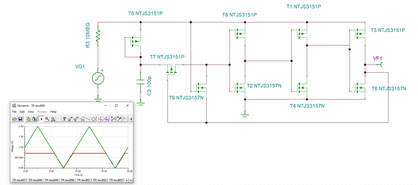
After crossing the input threshold voltage, I can either get a steady high signal, as shown here, or by decreasing the value of R1 and increasing the value of C1, I can either make the output do a single sudden transition to zero volts, which then steadily rises afterward with increasing input voltage:
or I can make the output go into a rapid oscillation:
Tina TI has a preview mode, which is how I was able to spot the oscillation when the simulation progress had otherwise slowed to a crawl. Not sure, but maybe either the oscillation or else (more likely) VF1's sudden transition to zero at the voltage threshold on the prior plot might be useful for driving a charge pump or something?Oh, and if it isn't already clear, the green line is the VG1 triangle input voltage (which I'm using to approximate a "voltage sweep") and the brownish-red line is the voltage measured at the VF1 probing point.
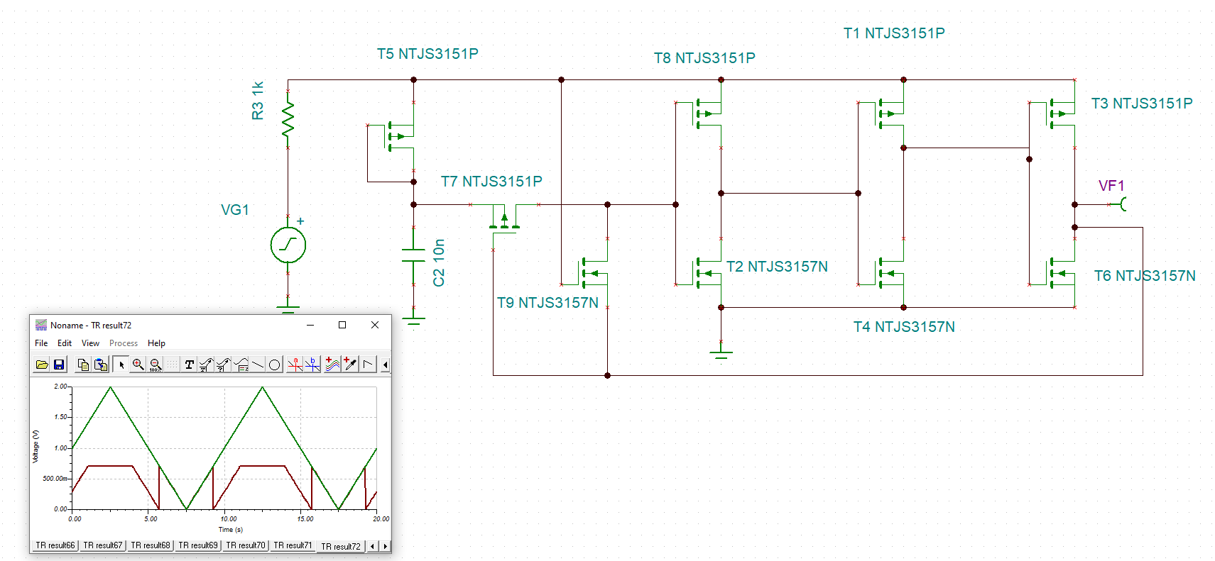
Salient Observation: The "regulated" voltage produced in this simulated circuit is around 700mv, not the ~100mv reported in the Bristol paper. I presume this has to do with the particular mosfets I happened to choose. Perhaps if I can find some mosfets that will produce the 100mv target reported in the Bristol paper, then the rest of the results will fall into place as well. I wish there existed a circuit simulator that could do a "component sweep" to automatically try out a bunch of different mosfets and see what their effects would be. It would gratly accelerate the process of identifying the most desirable component parts that could be used. Seems like it should be an "obvious" feature to have, and yet I'm not aware of any circuit simulators offering it.
Since 100mv is far below even the Vgs(th) of all the enhancement mosfets in both the digikey and mouser parts catalogs, this seems like yet another clue pointing toward the use of specialty mosfets, such as those by manufactured by ALD. Either that, or fets of a different type are being used.
Anyway, now that I have a circuit simulator up and working and producing results fairly quickly (unlike LTSpice), it's time to move forward. Hopefully ALD has SPICE models for their parts (yup, for a few of them anyway: http://www.aldinc.com/view-pdf.php). If so, then plugging those in to the simulator to check the effect would seem to be the next step. I'd wager it's either that, or else maybe there are subthreshold effects that the spice simulators aren't modelling accurately.... I discount the later possibility because, well, it's 2020, and surely by now EE simulation tools are pretty well evolved to account for subthreshold effects?
Edit5: FFS, their POS spice models (last updated in year 2004) won't load into TINA. :angry: Do they load into NGSpice?
Edit6: Well, using this: https://e2e.ti.com/support/tools/sim-hw-system-design/f/234/t/515230, I was able to fix ALD's stone-age spice file. And now it loads into TINA without complaint. But why the heck does it default to VTN=-0.037. I thought VTN was the threshold voltage for an n-channel mosfet, in which case shouldn't it be a positive number?
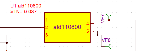
Edit7: Well, no answer to that question, but I can confirm that VTN is the threshold voltage.
Edit 8: Taking another look at the UB20M datasheet (https://www.bristol.ac.uk/media-library/sites/engineering/research/eem-group/zero-standby/UB20M_Datasheet_Rev.1.5.pdf), I'd have to say that the very low pico-amps static current number that's advertised is a bit misleading without the context provided by Figure 2,which appears to show that the input must be capable of generating a couple of nanoamps at the threshold voltage in order for the voltage to be detected. So if, hypothetically, under particular lighting conditions a small solar panel could produce at most 1na of short-circuit current, it still wouldn't have enough to get detected no matter how large it's open circuit voltage. That said, UB20M still does appear to be the best of breed, if only it were available.
-
Answering my own question, I designed a circuit using "real" mosfets from the generic LTSpice library and got a nice snap transition on a "voltage detector", all while drawing less than 300picoamps:
So, that's a simulated proof of concept. Now I just need to pull the trigger voltage down to a lower number, and I suspect that may involve using mosfets that aren't in the generic LTSpice catalog.Edit1: Ignore this particular circuit diagram. It turns out to be reducible to a much simpler circuit that draws even less current. I'm leaving it posted as a reference point for my own project tracking, but if not for that I would delete it.
Edit2: Lately LTSpice has, more often than not, failed to converge now that I have it simulating "real" mosfets. As a result I've started to look into TI's Tina circuit simulator, which AFAIK is also built on a SPICE platform. Although it's too soon to draw completely fair apples-to-apples comparisons, my initial impression is that TI Tina is much, much faster than LTSpice and also much better at converging. I'll update if that opinion changes.
Edit3: I've upgraded to using NTJS3151P and NTJS3157N as the simulation mosfets because they have lower threshold voltages and mouser has SPICE models for them that are free to download. I'm not yet endorsing them though, because it's just too early to say. They are just my first attempt, and there may be (probably are) better choices to be found. I'm finding it quite easy to import SPICE component models into TINA TI. I notice that some manufacturers, like Diodes Inc., actually rank their SPICE models as to how realistic they are.
@Mishka Which mosfets are you simulating? Head's up: I'd encourage you to find some real world simulated mosfets (you'll have to eventually anyway), because I'm found that, at least in LTSpice, the generic mosfets behave much, much differently than the apparently real-world simulated mosfets. Not sure why that would be so, but maybe their idealized nature are a little too idealized to be realistic in these types of circuits.
TINA TI lacks the convenience of a voltage sweep like LTSpice has, so I'm using a very low frequency triangle wave to approximate it.
Edit4: I'm starting to make progress with TI Tina towards simulating the original (Figure 5) circuit:
After crossing the input threshold voltage, I can either get a steady high signal, as shown here, or by decreasing the value of R1 and increasing the value of C1, I can either make the output do a single sudden transition to zero volts, which then steadily rises afterward with increasing input voltage:
or I can make the output go into a rapid oscillation:
Tina TI has a preview mode, which is how I was able to spot the oscillation when the simulation progress had otherwise slowed to a crawl. Not sure, but maybe either the oscillation or else (more likely) VF1's sudden transition to zero at the voltage threshold on the prior plot might be useful for driving a charge pump or something?Oh, and if it isn't already clear, the green line is the VG1 triangle input voltage (which I'm using to approximate a "voltage sweep") and the brownish-red line is the voltage measured at the VF1 probing point.
Salient Observation: The "regulated" voltage produced in this simulated circuit is around 700mv, not the ~100mv reported in the Bristol paper. I presume this has to do with the particular mosfets I happened to choose. Perhaps if I can find some mosfets that will produce the 100mv target reported in the Bristol paper, then the rest of the results will fall into place as well. I wish there existed a circuit simulator that could do a "component sweep" to automatically try out a bunch of different mosfets and see what their effects would be. It would gratly accelerate the process of identifying the most desirable component parts that could be used. Seems like it should be an "obvious" feature to have, and yet I'm not aware of any circuit simulators offering it.
Since 100mv is far below even the Vgs(th) of all the enhancement mosfets in both the digikey and mouser parts catalogs, this seems like yet another clue pointing toward the use of specialty mosfets, such as those by manufactured by ALD. Either that, or fets of a different type are being used.
Anyway, now that I have a circuit simulator up and working and producing results fairly quickly (unlike LTSpice), it's time to move forward. Hopefully ALD has SPICE models for their parts (yup, for a few of them anyway: http://www.aldinc.com/view-pdf.php). If so, then plugging those in to the simulator to check the effect would seem to be the next step. I'd wager it's either that, or else maybe there are subthreshold effects that the spice simulators aren't modelling accurately.... I discount the later possibility because, well, it's 2020, and surely by now EE simulation tools are pretty well evolved to account for subthreshold effects?
Edit5: FFS, their POS spice models (last updated in year 2004) won't load into TINA. :angry: Do they load into NGSpice?
Edit6: Well, using this: https://e2e.ti.com/support/tools/sim-hw-system-design/f/234/t/515230, I was able to fix ALD's stone-age spice file. And now it loads into TINA without complaint. But why the heck does it default to VTN=-0.037. I thought VTN was the threshold voltage for an n-channel mosfet, in which case shouldn't it be a positive number?
Edit7: Well, no answer to that question, but I can confirm that VTN is the threshold voltage.
Edit 8: Taking another look at the UB20M datasheet (https://www.bristol.ac.uk/media-library/sites/engineering/research/eem-group/zero-standby/UB20M_Datasheet_Rev.1.5.pdf), I'd have to say that the very low pico-amps static current number that's advertised is a bit misleading without the context provided by Figure 2,which appears to show that the input must be capable of generating a couple of nanoamps at the threshold voltage in order for the voltage to be detected. So if, hypothetically, under particular lighting conditions a small solar panel could produce at most 1na of short-circuit current, it still wouldn't have enough to get detected no matter how large it's open circuit voltage. That said, UB20M still does appear to be the best of breed, if only it were available.
@NeverDie Nice reduce!
AFAIU, the C1+M2 N-MOS will keep the trigger M6+M10 input low, and the output will turn high as soon as input voltage will reach the Vth threshold for the M10. Please note, the output will be limited by the R3=10g, so the circuit is kind of a voltage detector only.
Have you tried it yet? How about making it oscillating? Also, could you explain please, what the M1 does?
Please also note, for some reason the original network has the C1 protected with diode built into the MP3 P-FET. This probably should to be simulated with a diode rather FET. How do you think, why they need it?
-
@NeverDie Nice reduce!
AFAIU, the C1+M2 N-MOS will keep the trigger M6+M10 input low, and the output will turn high as soon as input voltage will reach the Vth threshold for the M10. Please note, the output will be limited by the R3=10g, so the circuit is kind of a voltage detector only.
Have you tried it yet? How about making it oscillating? Also, could you explain please, what the M1 does?
Please also note, for some reason the original network has the C1 protected with diode built into the MP3 P-FET. This probably should to be simulated with a diode rather FET. How do you think, why they need it?
@Mishka I'm rethinking the global strategy to emphasize minimizing leakage currents above all else, even if it means accepting higher threshold voltages. It's tough, though, because none of the parametric search engines (like Digikey or Mouser) appear to allow mosfet searches based on leakage currents. It's in the datasheets, but not searchable as far as I can tell. And with tens of thousands of mosfets to choose from, there are far too many to methodically review manually. So far leakage currents of 100na to 1ua seem common, and I need to find some mosfets which are much, much less than that or else this project will be academic. Maybe there's a way to leverage that Vishay load switch you identified (https://www.vishay.com/docs/66597/sip32431.pdf). Not sure how to proceed at the moment until some suitable real-world low-leakage mosfets can be identified.
A FemtoFET would be at least some improvement over what's comon (http://www.ti.com/lit/ds/symlink/csd15380f3.pdf), but it still lists fairly large MAX leakage amounts with no indication as to what typical leakage might be.
Nexperia lists some low leakage mosfets: https://assets.nexperia.cn/documents/application-note/AN90009.pdf
but I'd like to find lower leakage than even those, if possible.Ideally low leakage and low threshold would go hand in hand, as lower voltages generally imply lower leakages also, at least for any given mosfet.
-
@Mishka I'm rethinking the global strategy to emphasize minimizing leakage currents above all else, even if it means accepting higher threshold voltages. It's tough, though, because none of the parametric search engines (like Digikey or Mouser) appear to allow mosfet searches based on leakage currents. It's in the datasheets, but not searchable as far as I can tell. And with tens of thousands of mosfets to choose from, there are far too many to methodically review manually. So far leakage currents of 100na to 1ua seem common, and I need to find some mosfets which are much, much less than that or else this project will be academic. Maybe there's a way to leverage that Vishay load switch you identified (https://www.vishay.com/docs/66597/sip32431.pdf). Not sure how to proceed at the moment until some suitable real-world low-leakage mosfets can be identified.
A FemtoFET would be at least some improvement over what's comon (http://www.ti.com/lit/ds/symlink/csd15380f3.pdf), but it still lists fairly large MAX leakage amounts with no indication as to what typical leakage might be.
Nexperia lists some low leakage mosfets: https://assets.nexperia.cn/documents/application-note/AN90009.pdf
but I'd like to find lower leakage than even those, if possible.Ideally low leakage and low threshold would go hand in hand, as lower voltages generally imply lower leakages also, at least for any given mosfet.
@NeverDie That's true, discrete transistors have not too thin parameters on paper. But assuming quite low voltages (about 3V) I'd expect those Nexperia and TI transistors may draw picoamps indeed. I think this is better to check with real devices. But assuming how small they are an evaluation board will be required. There are some, but it might be way cheaper yet more flexible to assemble such a module manually.
For convenience, the custom PCB may also contain circuit required to measure the leakage. Perhaps a low-leakage capacitor may be charged to some known value, then a MOSFET (or number of FOSFETS in parallel) would discharge it for some time, and then the voltage drop can derive leakage.
-
@NeverDie That's true, discrete transistors have not too thin parameters on paper. But assuming quite low voltages (about 3V) I'd expect those Nexperia and TI transistors may draw picoamps indeed. I think this is better to check with real devices. But assuming how small they are an evaluation board will be required. There are some, but it might be way cheaper yet more flexible to assemble such a module manually.
For convenience, the custom PCB may also contain circuit required to measure the leakage. Perhaps a low-leakage capacitor may be charged to some known value, then a MOSFET (or number of FOSFETS in parallel) would discharge it for some time, and then the voltage drop can derive leakage.
@Mishka Perhaps of relevance to your last point, I found a fairly similar looking circuit to the Figure 5 Bristol paper UB40M circuit. Not identical, but I think you'll recognize some common features, like cutting off the feedback after a threshold has been reached and the use of n-channel and p-channel mosfet pairs configured as inverters:
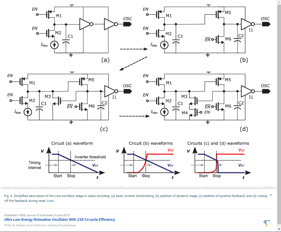
It's a bit different in that it's an oscillator circuit (not too surprising, as I showed above that the Bristol circuit can be made to oscillate also), but what's comforting is the authors claim it consumes just 4.2picowatts.

However, having become a bit jaded by now, I do wonder whether that 4.2 picowatts reflects only the supply current or whether it includes the leakage currents as well. :face_with_rolling_eyes: If it's the "all in" number, then maybe it's better than the Bristol design. I'm guessing that when they say their design minimizes "short circuit current," they are referring to leakage current (?), and if so, that would maybe be directly helpful to the problem of avoiding too much leakage currents in whatever discrete component circuitry you and I might settle on. -
@NeverDie That's true, discrete transistors have not too thin parameters on paper. But assuming quite low voltages (about 3V) I'd expect those Nexperia and TI transistors may draw picoamps indeed. I think this is better to check with real devices. But assuming how small they are an evaluation board will be required. There are some, but it might be way cheaper yet more flexible to assemble such a module manually.
For convenience, the custom PCB may also contain circuit required to measure the leakage. Perhaps a low-leakage capacitor may be charged to some known value, then a MOSFET (or number of FOSFETS in parallel) would discharge it for some time, and then the voltage drop can derive leakage.
@Mishka said in 💬 The Harvester: ultimate power supply for the Raybeacon DK:
@NeverDie That's true, discrete transistors have not too thin parameters on paper. But assuming quite low voltages (about 3V) I'd expect those Nexperia and TI transistors may draw picoamps indeed. I think this is better to check with real devices. But assuming how small they are an evaluation board will be required. There are some, but it might be way cheaper yet more flexible to assemble such a module manually.
For convenience, the custom PCB may also contain circuit required to measure the leakage. Perhaps a low-leakage capacitor may be charged to some known value, then a MOSFET (or number of FOSFETS in parallel) would discharge it for some time, and then the voltage drop can derive leakage.
I spoke too soon regarding the femtofets: they're frickin tiny, at about 0.6mm^2. That's not good from the standpoint of minimizing leakage current:
Edit1: I couldn't find a SPICE model for either Vishay SiP32431 or SiP32432. I sent an inquiry to Vishay, but I don't have high hopes they'll produce one. :disappointed: It has great specs though, so thank you for bringing it to my attention. Prior to learning of it I had been using http://www.ti.com/lit/ds/symlink/tps22860.pdf, which I had found to be a very handy chip. Ironically, it doesn't have a SPICE model either! Gosh, what is wrong with these manufacturers? Are they really too cheap/lazy to spice model their own chips, or is there some other reason for not making SPICE models readily available for every product in their catalog?
Edit2: I've converted over to using the ALD "subtreshold" n-channel and p-channel mosfets. I had to hack the spice files to get Tina TI to import the spice models. Hopefully I was able to preserve their accuracy.
Edit3: What's interesting is that even after substituting the super sensitive ALD parts into the circuit, the trigger voltage remains about 700mv.
Maybe the 700mv is a reflection of the particular ALD mosphets that I included in the simulation. This was just the first attempt. Maybe different ALD mosfet choices would yield a lower trigger voltage for the circuit.Edit4: I received a reply from Vishay regarding their load switch. It reads: " Unfortunately, we don’t have its SPICE model. Internally it is a P-ch switch, gate is injected with a constant current during turn on."
-
Some modest progress. If the TINA TI simulator is to be believed, then this circuit:
delivers a very clean 1 second pulse at VF2 about once every 10 minutes while consuming an average of about 6na. The one big caveat though is that it requires a 2v supply voltage.It's mainly noteworthy in comparison to TI's TPL5xxx timer, which consumes about 6x more current.
The main objective was to have a very low power timer circuit that could wake up infrequentlly to briefly invoke a conventional voltage detection circuit, which in turn could activate an energy harvester to process the energy captured and stored on a capacitor, provided there was enough charge on the capacitor to justify it. This does seem like a good step in that direction, though it would, of course, be preferable to have a circuit which consumes mere pico amps instead of nanoamps.
If nothing else it would perhaps make for a very low energy wake-up timer for a wireless sensor device. Alternatively, maybe it could form the start of a discontinuous charge pump circuit.
It would be interesting to build the circuit as a check on the simultator's accuracy and also just to see if it actually works.
Just a WAG, but I'm guessing that upgrading the circuit to use transistors which have a higher beta and reduced leakage currents will allow the circuit to still function while consuming even lower supply currents.
Edit1: Also, if I were to use gallium arsenide transistors (or whatever other transistors that have a lower forward voltage drop), it should run at a lower voltage. Perhaps a lower current as well? No idea, as I've never looked into gallium arsenide transistors before.
Hello! It looks like you're interested in this conversation, but you don't have an account yet.
Getting fed up of having to scroll through the same posts each visit? When you register for an account, you'll always come back to exactly where you were before, and choose to be notified of new replies (either via email, or push notification). You'll also be able to save bookmarks and upvote posts to show your appreciation to other community members.
With your input, this post could be even better 💗
Register Login