2 channel in wall dimmer
-
I like the project very much.
How are you sure that this hardware circuit is suitable and safe to give stable output ? I am asking that because I studied electronics but still see that a lot of knowledge are missing to implement such circuit. so, how did you learn this ? This is not a normal full wave rectifier :) It looks professional
Thanks.
-
Very nice Denke,
I suspect this unit is going to be mounted in wall behind the existing switch and wonder if existing switch can be used to control the dimming. The switch have to have spring return naturally.
Excellent work
Goran -
@Denke Can you share your files for this design?
It would be awesome and this looks great! -
Hi all
I will try to answer your questions.Q: what sort of switch would be on the wall?
For this design i would recommend that you use 230 V rated switch to control the dimmer. The output is still only 0V that you switch on and off. But the design is made in such a way that if you get short circuit on the capacitor in series in to the rectifier there can be 230 V on the input pins ( very unlikely because of other things will burn) but it can happen.Q: How are you sure that this hardware circuit …….
Doing a little benchmark and understand how dimmers and switches from NEXA or similar are working. Actually I ripped them apart and found out that they were using transformer less designs. From that I Googled this and read up on the topic as well as discussed this with colleges of mine. I then changed some parts as the transformerless design would in simulation not give more than 10mA so I added the MAX 17552 circuit in between and set the input voltage to 24 V with the zener diode and by that I will be able to draw about 30 mA (starting current of the circuit that I tested is around 24 mA).
Q: I suspect this unit is going to be mounted in wall behind……..
Yes of course but just use it as the switch, what I mean is that don’t use at ordinary switch were 230 V is applied. The circuit is designed to just feel a logic zero on one of the inputs. ( just make sure that you read my first reply above for safety reasons)
Q: can we control Celling fan using this dimmer.
Should not be a problem as I have used Triacs that are made for inductive load (not tested though). But the fan should not consume more than 4A. I also have not tested from a heat perspective how much power I can have running in the system. It might be less than the 2 channels times 4A. -
I have not descided yet if this is something i will sell or not so before i take that descision i will not share the actual design files but I will be happy to answer questions around the design and the considerations i have taken.
I might post a question later on if someone wants to join on first ordering for the prototypes/functional version, as this is the first step, primaraly to equip my house with these gadgets. In such a case i will offer those dimmers for a very low cost
-
So, what is the problem of sharing design as open hardware and at the same time sell your boards assembled?
-
Thanks for answering.
I have a question regarding dimmer circuit. I read that these circuits needs EMI filter. Is this something else rather than adding a snubber circuit ?
This issue I found in this link : http://hackaday.com/2015/04/19/switch-mains-power-with-an-esp8266/
the TRIAC will dump out a ton of EMI (that’s why most commercial dimmers have to have a choke in series with the load to be able to get FCC certification).
@ahmedadelhosni
Hi This circuit is not tested yet and can as you describe put out some or as stated a lot of EMI (Electro Magnetic Interference). I have not yet taken this in to account when designing this but have had it in the back of my head for something to look in to.The snubber circuit is more to protect agains "current rush" when you switch of an inductive load. This is actually something you use on the 5 volt side of relays to protect the transistor from breaking down. Andyou should also use on the output side of a relay for example if the cable you are runnigng is long or you want to switch of an inductive load
-
@ahmedadelhosni
Hi This circuit is not tested yet and can as you describe put out some or as stated a lot of EMI (Electro Magnetic Interference). I have not yet taken this in to account when designing this but have had it in the back of my head for something to look in to.The snubber circuit is more to protect agains "current rush" when you switch of an inductive load. This is actually something you use on the 5 volt side of relays to protect the transistor from breaking down. Andyou should also use on the output side of a relay for example if the cable you are runnigng is long or you want to switch of an inductive load
@Denke clear enough. Thanks
-
Hello @Denke , any updates about your progress ?
-
This will make your box less
https://ac-dc.power.com/products/linkswitch-family/linkswitch-tn/ -
This will make your box less
https://ac-dc.power.com/products/linkswitch-family/linkswitch-tn/ -
Hello @Denke , any updates about your progress ?
@ahmedadelhosni Going slowly at the moment had to do a respin on my thermostat project as i have made some small errors. Some of the design is the same so i will verify some things on the other design. Also waiting for chinese new years to end
-
@ahmedadelhosni Going slowly at the moment had to do a respin on my thermostat project as i have made some small errors. Some of the design is the same so i will verify some things on the other design. Also waiting for chinese new years to end
@Denke Yeah the holiday takes a long period there :)
Actually yesterday I read a lot about AC-DC converters and really learned new things, but I may need your help in clarifying some points please. I watched this video which guided me to this type of circuit design. Modlet Smart-Outlet Teardown and Review - (IT'S A POS)
Be aware that by this type of design with the transformer less design considerations needs to be taken when connecting computers and other stuff.
1- What I learned yesterday is that a "transformless" design is not safe ( don't know to what level of safety though ), but I read that there is no isolation between Main inputs and low voltage.
My questions:- Is this normal ? Would that affect the Atmega and other components ?
- How to avoid this ?
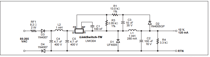
2- The above video mentioned that the Modlet outlet uses LNK304DN Datasheetwith outputs 12V. The below picture is from the datasheet and that reference was even used in the Modlet outlet as mentioned in the video.
My question:
- There are different designs in the datasheet but I can't diffrentiate between them and what is the best to use, but in all cases, this design still lacks the safety procedures, correct ? Like there is no MOV, Fuse .. ? It is just the circuit to produce a 12V 120mA which shall be stable and not noisy. Correct ?
3-
The AC is on the left hand side. the 0.33 uF capacitor in series on the 240 sets the maximum current, which should be around 10 mA on the AC side
I then changed some parts as the transformerless design would in simulation not give more than 10mA so I added the MAX 17552 circuit in between and set the input voltage to 24 V with the zener diode and by that I will be able to draw about 30 mA (starting current of the circuit that I tested is around 24 mA).
Can you explain what the 0.33 uF does to set the maximun current ?- What is the maximum current and how was it calculated ?
- How can I increase the output current to 100mA 5v/3.3v ?
- Actually the schematic is not clear at all when I download the pictuers. Maybe resolution :)
Thanks a lot for your support.
-
@Denke Very nice project! Hope to see a working protype soon. Any thoughts about making a relay switch based on this design. Will there be space and power for a 10A relay?
-
@Denke Yeah the holiday takes a long period there :)
Actually yesterday I read a lot about AC-DC converters and really learned new things, but I may need your help in clarifying some points please. I watched this video which guided me to this type of circuit design. Modlet Smart-Outlet Teardown and Review - (IT'S A POS)
Be aware that by this type of design with the transformer less design considerations needs to be taken when connecting computers and other stuff.
1- What I learned yesterday is that a "transformless" design is not safe ( don't know to what level of safety though ), but I read that there is no isolation between Main inputs and low voltage.
My questions:- Is this normal ? Would that affect the Atmega and other components ?
- How to avoid this ?
2- The above video mentioned that the Modlet outlet uses LNK304DN Datasheetwith outputs 12V. The below picture is from the datasheet and that reference was even used in the Modlet outlet as mentioned in the video.
My question:
- There are different designs in the datasheet but I can't diffrentiate between them and what is the best to use, but in all cases, this design still lacks the safety procedures, correct ? Like there is no MOV, Fuse .. ? It is just the circuit to produce a 12V 120mA which shall be stable and not noisy. Correct ?
3-
The AC is on the left hand side. the 0.33 uF capacitor in series on the 240 sets the maximum current, which should be around 10 mA on the AC side
I then changed some parts as the transformerless design would in simulation not give more than 10mA so I added the MAX 17552 circuit in between and set the input voltage to 24 V with the zener diode and by that I will be able to draw about 30 mA (starting current of the circuit that I tested is around 24 mA).
Can you explain what the 0.33 uF does to set the maximun current ?- What is the maximum current and how was it calculated ?
- How can I increase the output current to 100mA 5v/3.3v ?
- Actually the schematic is not clear at all when I download the pictuers. Maybe resolution :)
Thanks a lot for your support.
@ahmedadelhosni said:
My questions:
- Is this normal ? Would that affect the Atmega and other components ?
- How to avoid this ?
This is a matter of reference. When you have a power source with no contact to any othe rreference you are safe to touche one contact of that power source. If you make contact to the other one, you would be a resistor to the power source and act as esistor, having current runningthrough your body with all the negative impacts, including chance of death.
As explained, that is a matter of the reference. When you use a transformator, where secondary is not connected to anything else, you could safely make contact. In case you use any transfromless design, everything is somehow connected to mains. You are connected to grounds, so touching anything would be dangerous. As long as you do not touch anything, you are safe.
In fact a lot of electronics is tranformless with enough and safe insulation around it, so that no contact to grounds is possible. It is not only affecting persnal health, but could also be a source of fire if there could leak any current to grounds or mains from that circuitry. That's the reaosn for the insulation.In fact this applies to transformators as well, as the primay side has contact to grounds.
So, it does not affect any Atmel or so, it just raises the level of security precautions you have to take care of for this type of circuitry.
Hello! It looks like you're interested in this conversation, but you don't have an account yet.
Getting fed up of having to scroll through the same posts each visit? When you register for an account, you'll always come back to exactly where you were before, and choose to be notified of new replies (either via email, or push notification). You'll also be able to save bookmarks and upvote posts to show your appreciation to other community members.
With your input, this post could be even better 💗
Register Login