Powering mote 24/7 using only a supercap and solar
-
I suppose if worse came to worst, we could try answering the question empirically by using a test setup similar to this:
In this instance I partitioned the data ground from the power ground, and the two are not connected. However, via the header pins, a jumper could be connected between the two grounds. The experiment would be to try it both ways--connected vs. unconnected--and see which performs better.
-
The through holes on the stripped BQ25504 PCB (above)from Osh Park have too small a diameter to fit header pins into. In fact, it would require a very narrow gauge wire (narrower than what I have) to fit into it. So, unfortunately, I have doubts as to whether I will be able to test it, let alone use it.
This is all rather disappointing. :confounded: So far nothing about the BQ25504 has been easy.
-
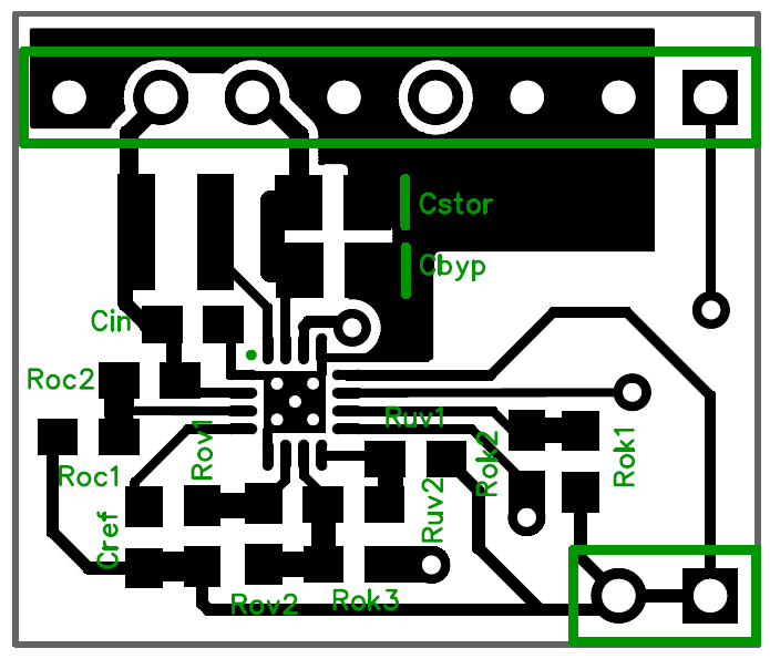
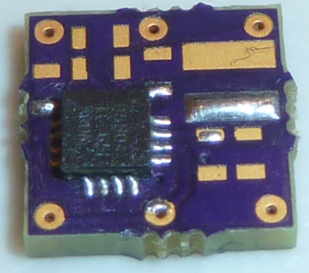
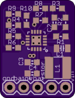
Not that it proves anything, but using KiCAD to look at the BQstripped PCB, I notice that the PCB designer chose to connect pins 12 and 13 both directly to each other and directly to the thermal pad.
-
Not that it proves anything, but using KiCAD to look at the BQstripped PCB, I notice that the PCB designer chose to connect pins 12 and 13 both directly to each other and directly to the thermal pad.
@NeverDie said:
Not that it proves anything, but using KiCAD to look at the BQstripped PCB, I notice that the PCB designer chose to connect pins 12 and 13 both directly to each other and directly to the thermal pad.
Did you say KiCAD? :+1: :+1: :+1:
-
@NeverDie said:
Not that it proves anything, but using KiCAD to look at the BQstripped PCB, I notice that the PCB designer chose to connect pins 12 and 13 both directly to each other and directly to the thermal pad.
Did you say KiCAD? :+1: :+1: :+1:
@blacey said:
Did you say KiCAD? :+1: :+1: :+1:
Yup. I had to use KiCAD to confirm the proper chip orientation before attempting to hand solder it to their PCB. Looks like a nice program.
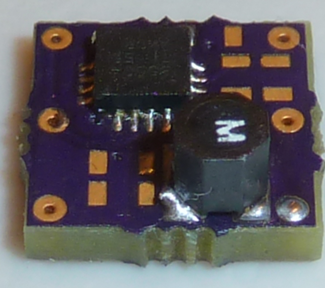
I had doubts I could hand solder the BQ25504, but I tried it using Dave Jones's tack and reflow method, and to my untrained eye it looks like it came out OK, despite the chip not being completely well aligned with the solder pads:
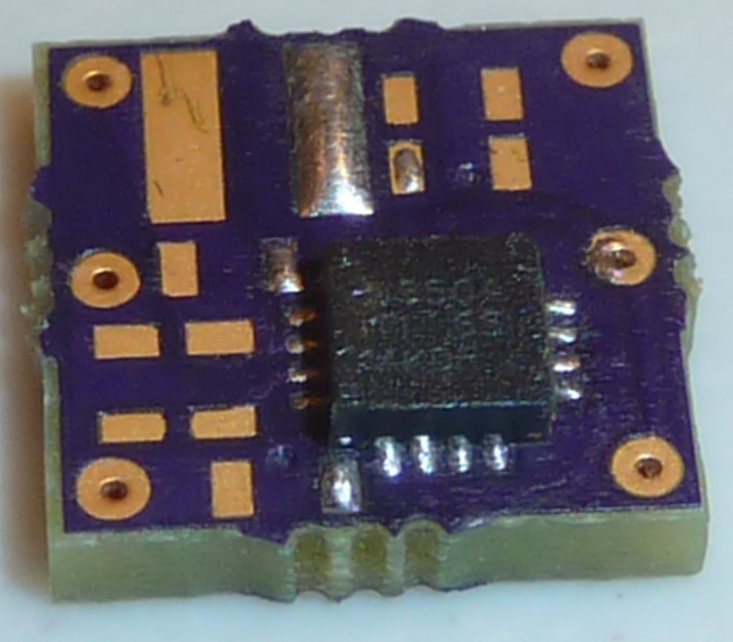
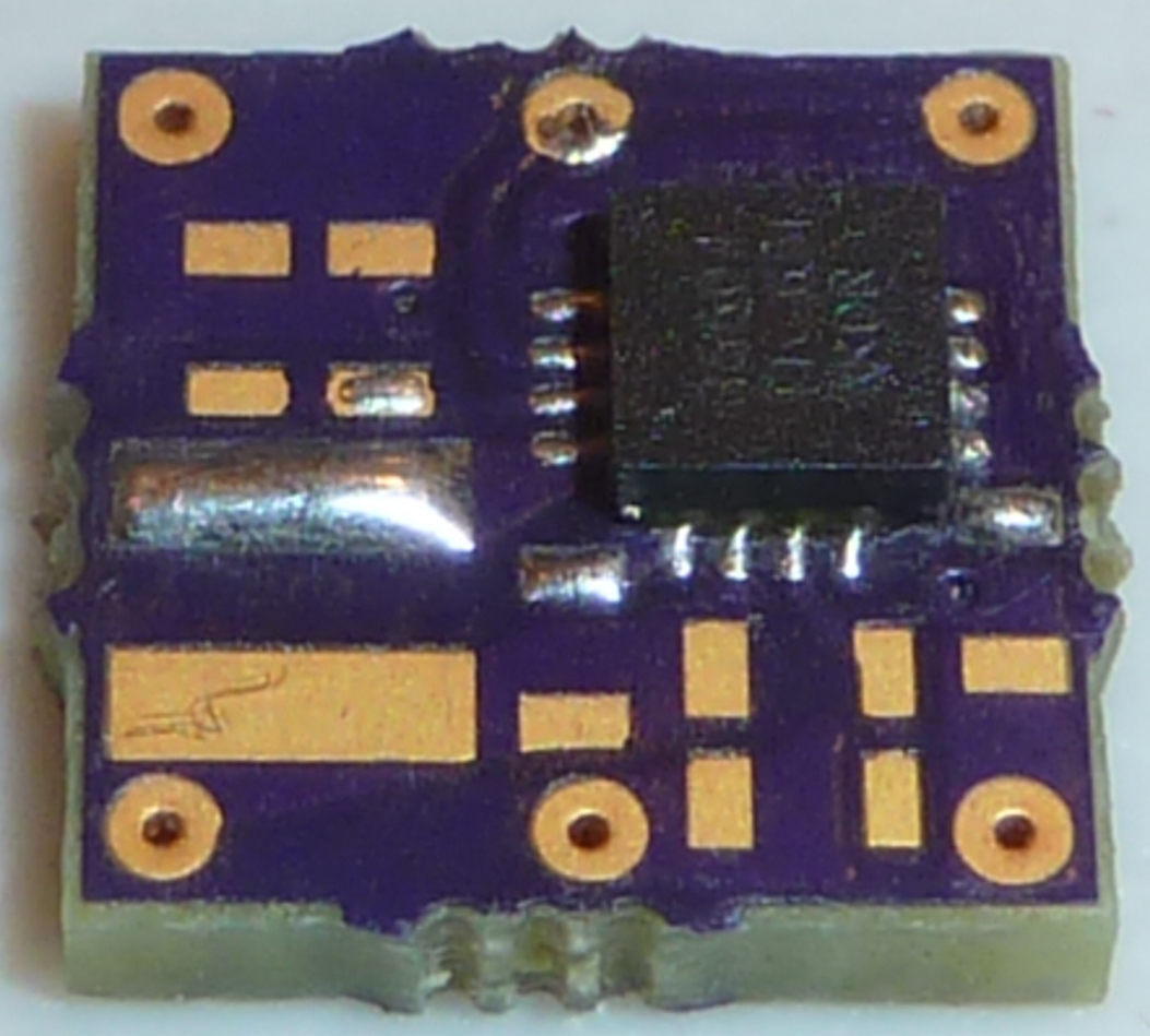
The Wurth inductors arrived today, so I'll have a go at soldering that on next. Hopefully the BQstripped PCB designer picked the same one I did!
-
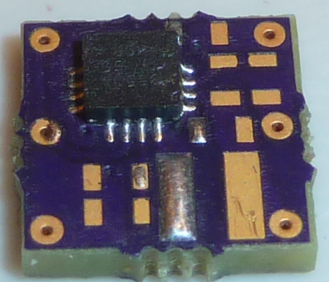
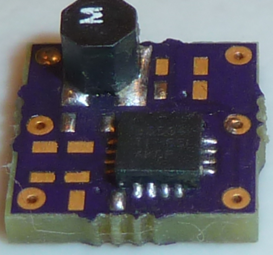
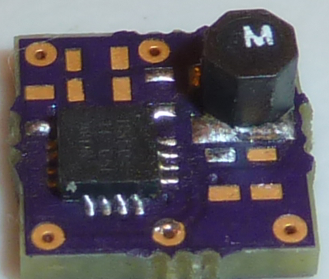
Looks as though the inductor hand soldered as well:
-
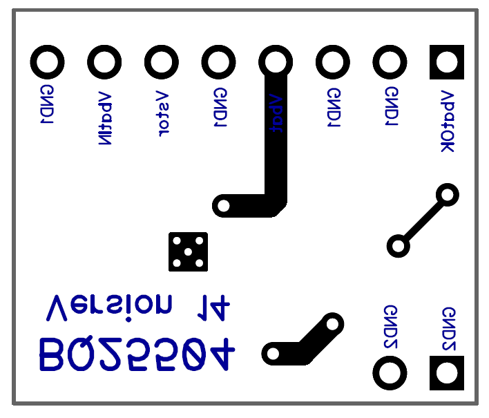
Interestingly, if one looks at the KiCad schematic for the bqstripped PCB, you will notice that it draws a distinction between regular GND and GNDPWR:
0_1480428663373_kicad_schematic.pdfHowever, as already noted, that distinction seems to be cast aside when they laid out the PCB traces, since pins 12 and 13 are connected together directly by a trace. Indeed, the schematic explicitly shows GNDPWR connected to GND. So, why create the distinction in the first place?
-
@NeverDie
this is for the power gnd plane regarding the analog gnd plane. analog for instance should be connected at one point. but then in practice like you said it looks a bit different...
don't worry too much i think!
The good in this, is i think, you have learnt good things (taking care of datasheet guidelines etc...) for future :thumbsup: -
I had to order some 4.7uF smd 0603 capacitors and 4.42M ohm 0603 resistors.
The DS also calls for 15.62M ohm resistors, but the closest thing that Digikey carries is 15M ohm 0603 smd's, so that's what I ordered.
Meanwhile I did solder the 10nf capacitors to the BQstripped pcb, as I had those on hand. If I had it to do over, I would probably have soldered them prior to soldering the BQ25504 and the 22uH inductor, as those parts were in the way.
-
I had to order some 4.7uF smd 0603 capacitors and 4.42M ohm 0603 resistors.
The DS also calls for 15.62M ohm resistors, but the closest thing that Digikey carries is 15M ohm 0603 smd's, so that's what I ordered.
Meanwhile I did solder the 10nf capacitors to the BQstripped pcb, as I had those on hand. If I had it to do over, I would probably have soldered them prior to soldering the BQ25504 and the 22uH inductor, as those parts were in the way.
Just a few notes on a conservative approach to component selection for boost converters that I've lately gleaned from reading various datasheets:
-
Ideally, capacitors should be rated X5R or X7R.
-
For inductors, generally speaking the lower the DCR the better, provided that the saturation current remains appropriately high enough. For instance, the B82462G4 series (http://www.digikey.com/product-search/en/inductors-coils-chokes/fixed-inductors/196627?k= +B82462G4&k=&pkeyword= +B82462G4&pv7=2&mnonly=0&newproducts=0&ColumnSort=0&page=1&quantity=0&ptm=0&fid=0&pageSize=500 ) has much lower DCR than any of the datasheet recommended inductors. These inductors are more expensive, but their use should, in theory, lead to higher efficiency and/or lower start/operating voltages. Also, I suspect the Tindie board's performance is impaired by its choice of inductor, because I haven't seen specs on any inductors as small as theirs is that has a low DCR.
-
-
+1 for X5R/X7R ;)
-
@scalz said:
+1 for X5R/X7R ;)
I looked into it a little bit more, and I'm defaulting to X7R for everything, unless there's good reason not to: https://www.maximintegrated.com/en/app-notes/index.mvp/id/5527 The article also provides good reason to favor larger package sizes, up to size 1210, if the design allows.
-
I've settled on this series of shielded inductor as having a good bang for buck ratio: low DCR, high current rating, and relatively low price: http://www.digikey.com/catalog/en/partgroup/dg-series/53965?mpart=1255AY-220M=P3&vendor=490
If anyone knows of a better series than that one, please post.
-
For comparison, I ordered an inexpensive ($0.91, including shipping) 6v panel: https://www.aliexpress.com/item/6V-0-6W-Solar-Power-Panel-Module-DIY-Small-Cell-Charger-For-Light-Battery-Phone-Toy/32723002222.html?spm=2114.13010608.0.0.OYll8L
It's a little bigger, but still reasonably small (a little more than 2"x3" in size). Mainly, though, the energy harvesting chips that work at very low voltages are surprisingly expensive, so maybe this higher voltage panel will allow the use of less expensive chips that have higher start voltages. Of course, indoors I don't expect it will ever get to a full 6v under load, but I do expect that under the same lighting conditions it will offer up higher voltages at the same load as the cheap garden solar cell referenced in the OP.
-
@scalz I was just now noticing that you like to put silkscreen between component pads:
Does silkscreen work the same as solder mask, in that it sorta "repels" molten solder away from it? I really don't know, but I've been assuming that it doesn't. In fact, I've gone out of my way to move silkscreen away from the solder pads out of fear it might contribute to inadvertent solder bridging between pads.
Anyone know?
-
@NeverDie
well, sometimes i think to not put them at all! especially when i want to make things compact..at a moment, it becomes difficult to fit them, and you can't reduce fontsize because it's ugly. usually, i use 32mils.I've never had short because of this though.
-
@NeverDie
well, sometimes i think to not put them at all! especially when i want to make things compact..at a moment, it becomes difficult to fit them, and you can't reduce fontsize because it's ugly. usually, i use 32mils.I've never had short because of this though.
@scalz said:
@NeverDie
well, sometimes i think to not put them at all! especially when i want to make things compact..at a moment, it becomes difficult to fit them, and you can't reduce fontsize because it's ugly. usually, i use 32mils.I've never had short because of this though.
Actually, I wasn't referring so much to the letters and numbers--which are off to the side-- so much as the little dashes and lines that appear between the pads. The letters and numbers are useful.
-
I know, you're right, these are useful ;)
but when doing compact stuff, it's not always easy to display everything well..
I usually have my computer display in front of me when assembling, or i print the layout x4..so i don't look at the silkscreen so much..About "repels", if i understand right, i have never got short during soldering. I think you mean silkscreen, between parts, would help to bridge soldering? but no never got problem.
I often use stencil+reflow oven, so there is only the solder needed. For proto, generally i almost assemble at hand, still no problem :)
Hello! It looks like you're interested in this conversation, but you don't have an account yet.
Getting fed up of having to scroll through the same posts each visit? When you register for an account, you'll always come back to exactly where you were before, and choose to be notified of new replies (either via email, or push notification). You'll also be able to save bookmarks and upvote posts to show your appreciation to other community members.
With your input, this post could be even better 💗
Register Login