CNC PCB milling
-
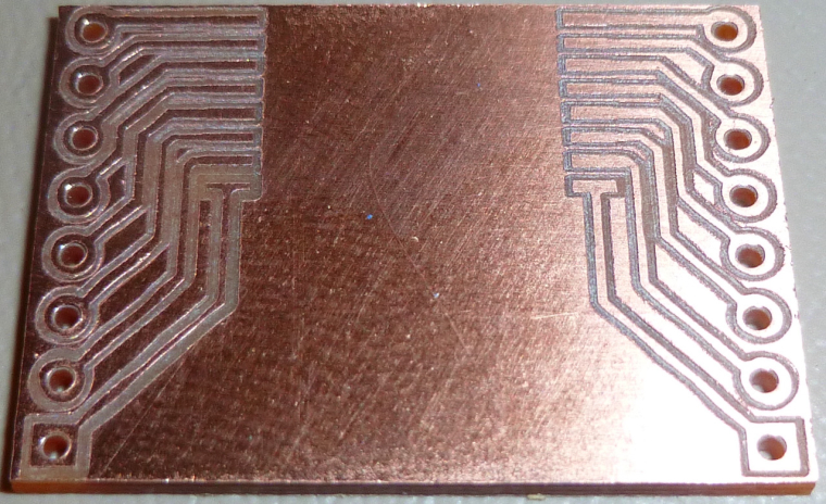
I did the top layer, together with alignment holes, for a real FR4 PCB:
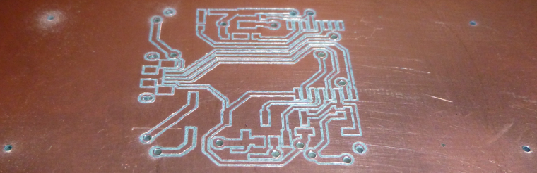
As an experiment, I thought I would standardize on 0.9mm holes for the through-holes, via-holes, and alignment holes, so that there would be fewer tool changes. Looks like it will work, but, meh, I think I'll use smaller via holes in the future.Out of time for today, so I plan to etch the flip side tomorrow.
@neverdie 0.4-0.5mm for vias using 0.3mm silver plated "wrapping wire". 0.9 for TH and alignment holes.
Tomorrow redo the alignment holes on the sacrificial layer so you get perfect alignment (if you don't have homing endstops, as I don't) and put the pins in and sick the pcb after that, be careful how you flip the board, I tend to use asymmetric alignment holes so I can only flip it one way (; -
Argh, it just occurred to me that I was premature in drilling the TH and via holes, because they may seriously interfere with the autoleveling when I etch the reverse side. This must be why @andrew etches the mirrored bottom side first, so that when it's flipped the top side can be etched and then drilled.
-
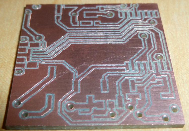
Re-using the alignment holes already drilled, I flipped over the PCB and etched the mirrored bottom. It worked! Some of the traces are only as thick as a hair, but they all conduct and none are broken.
I guess I'll have to flip it again in order to route the board outline. So, count that as yet another reason to start by etching the bottom first.
I had to autolevel at 6mm in order to dodge all the holes I had prematurely drilled, so perhaps that's why this particular etching came out so uneven. -
Re-using the alignment holes already drilled, I flipped over the PCB and etched the mirrored bottom. It worked! Some of the traces are only as thick as a hair, but they all conduct and none are broken.
I guess I'll have to flip it again in order to route the board outline. So, count that as yet another reason to start by etching the bottom first.
I had to autolevel at 6mm in order to dodge all the holes I had prematurely drilled, so perhaps that's why this particular etching came out so uneven.@neverdie the order of the process should be the following:
- drilling the alignment holes (through the PCB into the sacrificial layer)
- fixing the pcb with the alignment pins/headers
- isolation routing on the bottom layer
- flipping the pcb
- isolation routing on the top layer
- drilling holes on the top layer
- milling the pcb outline on the top layer
as I see your results, you could use alignment holes closer to your actual design's border, but it should be definitely out of the pcb's edge + milling tool width area.
the very thin traces are most probably caused by:
- moving and not stable pcb
- improperly calculated tool width
- improper autoleveling on the given side
-
How do I mill a slot? Do I treat it the same as a regular hole, except use a routing bit rather than a drill bit when it comes time to cut the slot?
@neverdie said in CNC PCB milling:
How do I mill a slot? Do I treat it the same as a regular hole, except use a routing bit rather than a drill bit when it comes time to cut the slot?
you can mill holes, which are bigger than your drill bits, you can find a milling section in flat cam when you are working with the drill file.
you can mill slots as well, for this the slot has to be designed properly in the PCB designer software. you have to draw closed shapes on e.g. the edge cuts layer, then basically you have to follow the same approach in flatcam that is used to create the edge milling cnc job, but instead of the edge lines, you have to select the slots.
if you design it that way, then you can do both the slot and edge milling at once. -
I drilled the alignment holes with 0.8mm diameter. I'm using regular male header pins for the alignment, and having tried it, I think 0.8mm is really too tight. Not sure how @andrew is using 0.7mm. Different pins I guess? Anyhow, next time I'll try 0.9mm hole diameter.
@neverdie said in CNC PCB milling:
I drilled the alignment holes with 0.8mm diameter. I'm using regular male header pins for the alignment, and having tried it, I think 0.8mm is really too tight. Not sure how @andrew is using 0.7mm. Different pins I guess? Anyhow, next time I'll try 0.9mm hole diameter.
maybe my pins also have different factors, but indeed, the given holes are pretty tight. this helps to prevent unnecessary pcb movements, which is very important if you work with 6mil traces/isolation, as a small unwanted movement could result in wasted pcb. if you work with bigger traces/clearings then it is not as important.
I would recommend to stick to one size which is good for your selected pins and which does not let the pcb to move.
-
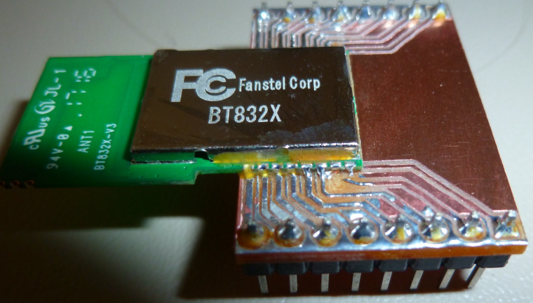
Here's the final product:
Three of the vias are located under an SMD module, so I'll just have to try to minimize any solder bumps over them. -
Here's the final product:
Three of the vias are located under an SMD module, so I'll just have to try to minimize any solder bumps over them.Unfortunately, even a tiny solder bump prevents the module from being soldered. I would have to redesign this so that the vias are not under the module.
-
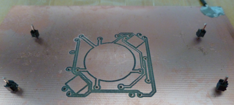
Another good thing for people to know is that you can leave a single-sided blank PCB installed in the CNC and then, as the need arises, cut out additional modules from it:
For instance, this morning I cut this module carrier out of the above, already used, copper clad PCB:
So, for simple small things, it's a handy arrangement, and the incremental cost is negligible.
-
Another good thing for people to know is that you can leave a single-sided blank PCB installed in the CNC and then, as the need arises, cut out additional modules from it:
For instance, this morning I cut this module carrier out of the above, already used, copper clad PCB:
So, for simple small things, it's a handy arrangement, and the incremental cost is negligible.
@neverdie Perhaps a clearer explanation ?
-
One problem I've run into though is that the foil traces can sometimes lift up in the course of ordinary soldering. For instance, the traces connecting the second to the right pin on the Fanstel module seems to have utterly disappeared, leaving that pin unconnected:
Maybe it's the quality of the blank PCB? I just don't know. -
@neverdie It looks like you could potentially make those traces just a touch wider looking at the receiving end of the module. Woulld that be an option?
@dbemowsk said in CNC PCB milling:
Woulld that be an option?
Maybe: I'll try a 10 degree bit and tighter autoleveling to see if that gives wider traces.
-
@dbemowsk said in CNC PCB milling:
Woulld that be an option?
Maybe: I'll try a 10 degree bit and tighter autoleveling to see if that gives wider traces.
-
It's funny, because I redid the soldering using an altogether new board, and it failed in exactly the same place:
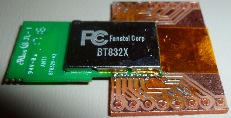
This time, though, you can actually see the copper trace has curled up away from the board. -
It's funny, because I redid the soldering using an altogether new board, and it failed in exactly the same place:
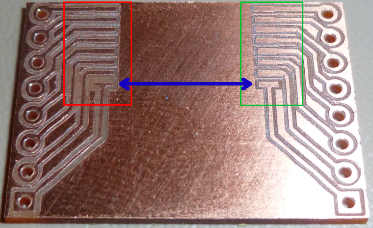
This time, though, you can actually see the copper trace has curled up away from the board.@neverdie It is quite odd that that one did it and some of the others didn't on that side of the board. Looking at your previous image, the pads and traces on the side marked in green look noticeably larger than the ones marked in red. Look at the ones marked with the blue arrow. It looks like those should, or at least could be the same size. Your thru hole pads on the left for the breakout headers also look smaller than the ones on the right. Shouldn't the two sides be a mirror image of each other?
-
@neverdie It is quite odd that that one did it and some of the others didn't on that side of the board. Looking at your previous image, the pads and traces on the side marked in green look noticeably larger than the ones marked in red. Look at the ones marked with the blue arrow. It looks like those should, or at least could be the same size. Your thru hole pads on the left for the breakout headers also look smaller than the ones on the right. Shouldn't the two sides be a mirror image of each other?
-
@dbemowsk It's because the left side of the board is higher than the righthand side, and apparently the autoleveling isn't working all that precisely.
@neverdie I can see that the left side looks like it cut deeper, which would cause that. I still think it is the thin traces though. Can you do any manual leveling of the bed? If so, I would attempt that. My Anet A8 3D printer, though not a CNC, is all manual leveling and I do have to check it from time to time.
-
@neverdie I can see that the left side looks like it cut deeper, which would cause that. I still think it is the thin traces though. Can you do any manual leveling of the bed? If so, I would attempt that. My Anet A8 3D printer, though not a CNC, is all manual leveling and I do have to check it from time to time.
@dbemowsk said in CNC PCB milling:
@neverdie I can see that the left side looks like it cut deeper, which would cause that. I still think it is the thin traces though. Can you do any manual leveling of the bed? If so, I would attempt that. My Anet A8 3D printer, though not a CNC, is all manual leveling and I do have to check it from time to time.
I suppose I could shim under the sacrifice board with slips of paper to get the right height.
I would have thought that the autoleveling would have accurately compensated though. Not sure why it isn't, especially if I'm autoleveling at 2mm spacing. Maybe this is an area where a future version of the GRBL driver will get it right.
Hello! It looks like you're interested in this conversation, but you don't have an account yet.
Getting fed up of having to scroll through the same posts each visit? When you register for an account, you'll always come back to exactly where you were before, and choose to be notified of new replies (either via email, or push notification). You'll also be able to save bookmarks and upvote posts to show your appreciation to other community members.
With your input, this post could be even better 💗
Register Login