💬 The Harvester: ultimate power supply for the Raybeacon DK
-
I put David Johnson's 3na oscillator circuit:
http://www.discovercircuits.com/DJ-Circuits/3na-osc.htm
into LTSpice and ran the simulation, and it looks promising:
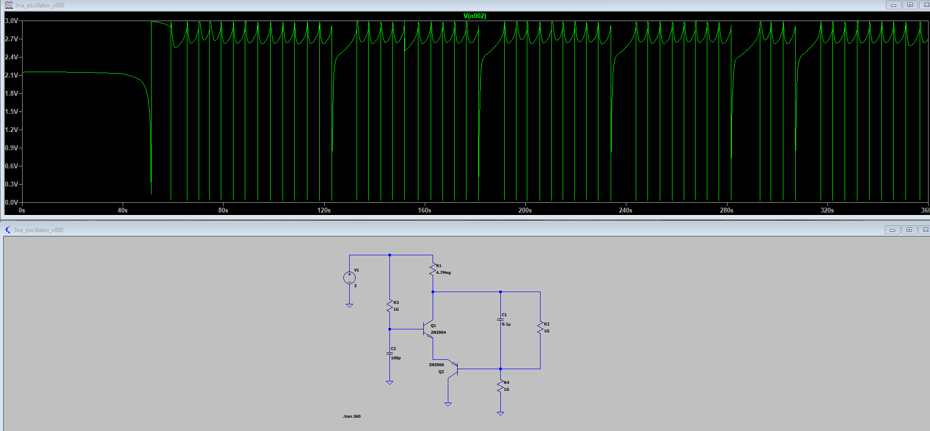
It also runs just fine at 2v. Fairly easy to get a shorter or longer cycle by tweaking the resistor values and/or capacitor values.
The voltage swing is even better than I was expecting: it drops all the way down to around 30 or 40mv. :yum:
Of course, it would be nice if it could run at even lower voltages than 2v. Seems like that should be possible. Anyone have suggestions for which transistors to try for that?
The simulation shows that there's a very nice current pulse of about 4.2ma through Q2 during the very brief discharge phase, so I'm guessing that could drive a buffer transistor to turn on hard, which in turn could, in theory, drive a meaningful load without disturbing the underlying timer circuit. :sunglasses: If that's the architecture, though, there may need to be a separate, isolated capacitor to drive the load that charges up in parallel with the capacitors in this oscillator circuit--unless perhaps there's some way to recycle/reuse the current that gets dumped and otherwise wasted during each discharge.
Or, quite possibly, it could be used to drive a flyback type circuit, in which case I possibly wouldn't need a commercial boost chip at all and could instead do all the boosting with a homemade DIY circuit made out of discrete components. :heart_eyes: That's the promise of what this type of low-level control could grant.
Edit: I posted the LTSpice circuit simulation file for David Johnson's 3 nano-ampere circuit here:
https://github.com/rabbithat/3nanoAmpOscillatorEdit2: I anticipate a potential problem though: the 3na oscillator has very high input impedance. PV cells are modeled as having a shunt resistance, and unless that shunt resistance is exceptionally high, then most of the generated solar cell current won't be entering into the oscillator but will instead be lost as wasted current through the shunt resistor. I'm hoping that doesn't preclude the oscillator from working, but it might if that reduced current translates into reduced voltage at the inputs to the oscillator. The best case scenario would be that the oscillator simply has a much longer cycle time with the PV cell as compared to a battery. In any case, shunt resistance doesn't seem especially easy to measure, so one strategy would be to just build the circuit and see how it works with the target PV cell rather than fuss too much over constructing an accurate equivalent circuit to plug into the simulator.
Edit3: Good news. Using the method published in IEEE to calculate PV shunt resistance (https://ieeexplore.ieee.org/document/1483817), I calculate the shunt resistance on the keychain solar cell to be 30,681,818 ohms. So, more than likely the oscillator will work when hooked up to it. This also finally explains why these solar cells perform so well at even ultra low lighting conditions.
This thread seems to have petered out, so I guess that's the end of it. It was nice while it lasted. :-)
Dear @NeverDie, you've done tremendous amount of work! The topic is extremely interesting, but I admit I can't keep up the pace, especially when discussion dived so deep and requires fair amount of research and simulation. Let's just keep it floating and open for everyone (I really hope David might kick it up). I personally try to follow up your recent posts a bit later, sorry :-(
P.S. Asked a colleague about it and he's like: "Nano... what?!" :)
-
@Mishka I recently had some convivial email exchanges with David Pilling after I reached out to him. He seemed interested in this thread, or maybe he was just being polite. Regarding his previous efforts, he mentioned that he was eventually able to run his PUT oscillator at 200 nanoamps.
-
Dear @NeverDie, you've done tremendous amount of work! The topic is extremely interesting, but I admit I can't keep up the pace, especially when discussion dived so deep and requires fair amount of research and simulation. Let's just keep it floating and open for everyone (I really hope David might kick it up). I personally try to follow up your recent posts a bit later, sorry :-(
P.S. Asked a colleague about it and he's like: "Nano... what?!" :)
@Mishka I've got good news, and I've got bad news. The bad news is that according to the LTSpice circuit simulator, the Dave Johnson circuit, as given, is nowhere near 3na of power consumption. It's much higher than that. Here's what it shows as the current passing through the R10 resistor in the figure below:
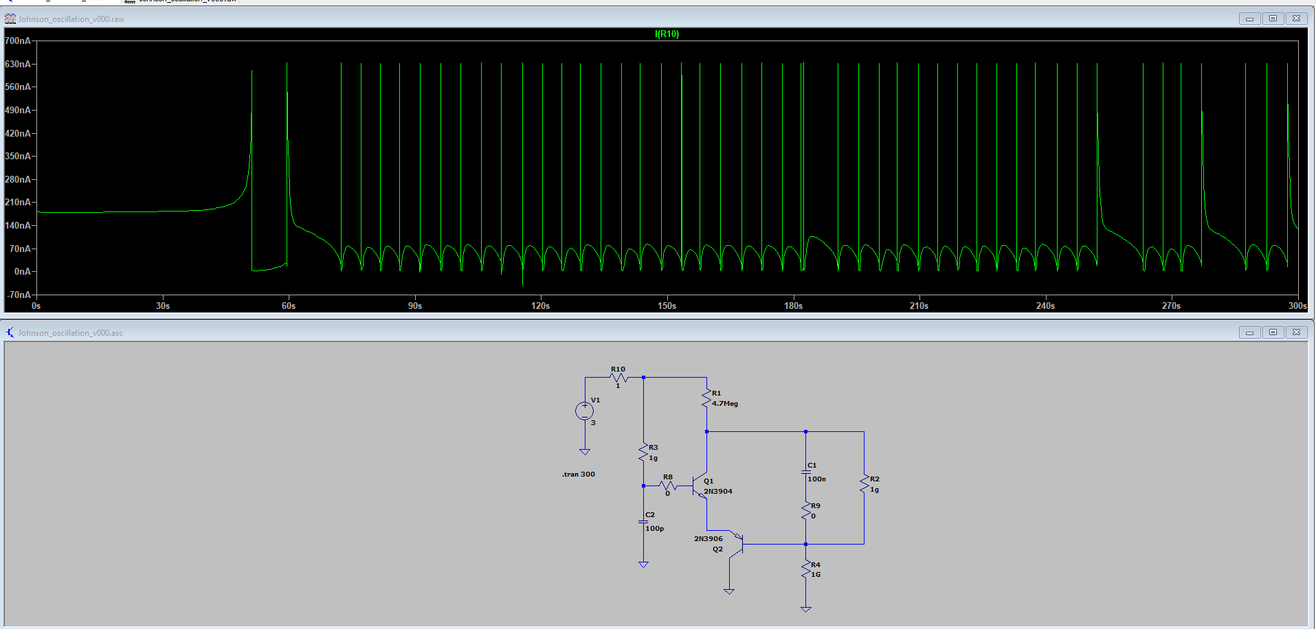
The good news is that by increasing the resistance and capacitance, I've confirmed it's possible to run the oscillator at 1 lux on the keychain solar cell:
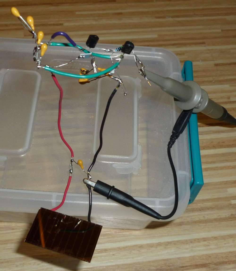
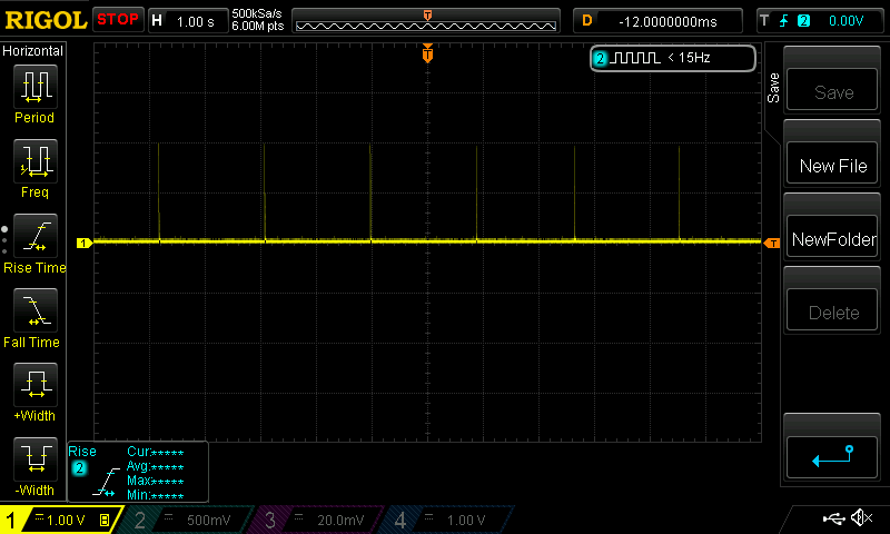
If measured at the output pin of transistor Q2, it produces a 2 volt pulse every couple of seconds:
I'm pretty confident it will run at even lower lux, al beit producing a lower voltage, but I'm not yet setup to test at less than 1 lux yet.
Here is an approximation of the modified circuit and its current consumption:
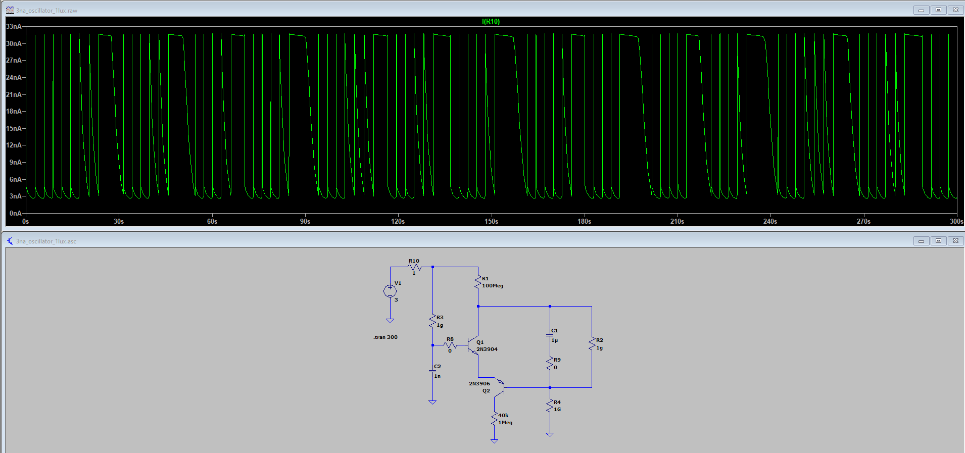
As you can see, both the average and the instantaneous current consumption are less than for TI's TLV5110 chip.And yes, I've confirmed through testing that it can self-start at 1 lux even if it had been pitch black prior! In that case it starts a pulse train at lower magnitude but higher frequency and gradually works it's way up to the 2 volt magnitude at the 0.5 Hz frequency, which at 1 lux is where it settles.
:smile: :smile: :smile: :smile: :smile:
-
@Mishka I've got good news, and I've got bad news. The bad news is that according to the LTSpice circuit simulator, the Dave Johnson circuit, as given, is nowhere near 3na of power consumption. It's much higher than that. Here's what it shows as the current passing through the R10 resistor in the figure below:
The good news is that by increasing the resistance and capacitance, I've confirmed it's possible to run the oscillator at 1 lux on the keychain solar cell:
If measured at the output pin of transistor Q2, it produces a 2 volt pulse every couple of seconds:
I'm pretty confident it will run at even lower lux, al beit producing a lower voltage, but I'm not yet setup to test at less than 1 lux yet.
Here is an approximation of the modified circuit and its current consumption:
As you can see, both the average and the instantaneous current consumption are less than for TI's TLV5110 chip.And yes, I've confirmed through testing that it can self-start at 1 lux even if it had been pitch black prior! In that case it starts a pulse train at lower magnitude but higher frequency and gradually works it's way up to the 2 volt magnitude at the 0.5 Hz frequency, which at 1 lux is where it settles.
:smile: :smile: :smile: :smile: :smile:
-
@Mishka The circuit is more stable and consistent than the 3v simulation would suggest. I'm now totally sold on the value of simulation, but it's a bit problematic when a solar cell/panel is involved because for an accurate simulation you need to find an accurate "equivalent circuit" to use in place of the cell/panel, and for accuracy that means a 5 element circuit: two diode, shunt resistor, series resistor, and a current source. However, figuring out the correct values for those parts requires a lot of measurements to get the desired accuracy and is a project in itself.
That said, I'm optimistic that there are some less mainstream transistors that will allow the circuit to run at lower voltage.
-
Here's a courtesy heads-up.
I just now stumbled across a circuit:

published here:
https://www.edn.com/solar-powered-motor-runs-on-10-na/
that allegedly can operate on as little as 10na while collecting energy, which it then uses to power a small pager motor once a threshold voltage is reached.It also has the virtue of utilizing inexpensive jelly bean parts and not relying on gigaohm resistors, which in the Dave Johnson circuit turned out to be so large that I lack the means to verify their specs through measurement after they are delivered.
This other guy instantiated the circuit as a PCB, and he made the gerber for it available as a free download: https://hackaday.io/project/159691-electron-bucket-extreme-power-management-module
If it turns out to be true that the circuit can both collect the current and trigger at a threshhold voltage all with just 10na of overhead, then on its face it sounds better than the David Johnson circuit turned out to be and possibly also better than many/most/(all?) of the commercial chips that we've reviewed on this thread if paired with an appropriate amorphous solar panel.
Edit:
But wait! There's more. There appears to exist an equivalent single chip voltage detector that also consumes a mere 10na of current: https://www.akm.com/content/dam/documents/products/power-management/power-ic-for-energy-harvesting/ap4405aen/ap4405aen-en-datasheet.pdf
It's itty bitty, so it's probably a great fit for your uber-compact design."But I want more!" I can hear you say. "I want a total step-up solution! And I want one that doesn't use a transformer!" Well, of course you do. Who wouldn't? Apparently, a 0.2v transformerless step-up solution does exist as well. I'm just not sure where. They developed it for a customer who wanted to harvest energy from... bacteria. Actually, the official term is "microbial fuel cell." The chip is the AP4470, and thankfully it can also be powered by solar, without bacteria.
https://solutions.akm.com/us/en/applications/energy-harvesting/
But can we buy it? Or is it just another inaccessible research project? I don't yet know. Can you read Japanese? The trail of bread crumbs written in English seems to run cold after the above link, but there's more about it that's written in Japanese. Argh. -
Here's a courtesy heads-up.
I just now stumbled across a circuit:
published here:
https://www.edn.com/solar-powered-motor-runs-on-10-na/
that allegedly can operate on as little as 10na while collecting energy, which it then uses to power a small pager motor once a threshold voltage is reached.It also has the virtue of utilizing inexpensive jelly bean parts and not relying on gigaohm resistors, which in the Dave Johnson circuit turned out to be so large that I lack the means to verify their specs through measurement after they are delivered.
This other guy instantiated the circuit as a PCB, and he made the gerber for it available as a free download: https://hackaday.io/project/159691-electron-bucket-extreme-power-management-module
If it turns out to be true that the circuit can both collect the current and trigger at a threshhold voltage all with just 10na of overhead, then on its face it sounds better than the David Johnson circuit turned out to be and possibly also better than many/most/(all?) of the commercial chips that we've reviewed on this thread if paired with an appropriate amorphous solar panel.
Edit:
But wait! There's more. There appears to exist an equivalent single chip voltage detector that also consumes a mere 10na of current: https://www.akm.com/content/dam/documents/products/power-management/power-ic-for-energy-harvesting/ap4405aen/ap4405aen-en-datasheet.pdf
It's itty bitty, so it's probably a great fit for your uber-compact design."But I want more!" I can hear you say. "I want a total step-up solution! And I want one that doesn't use a transformer!" Well, of course you do. Who wouldn't? Apparently, a 0.2v transformerless step-up solution does exist as well. I'm just not sure where. They developed it for a customer who wanted to harvest energy from... bacteria. Actually, the official term is "microbial fuel cell." The chip is the AP4470, and thankfully it can also be powered by solar, without bacteria.
https://solutions.akm.com/us/en/applications/energy-harvesting/
But can we buy it? Or is it just another inaccessible research project? I don't yet know. Can you read Japanese? The trail of bread crumbs written in English seems to run cold after the above link, but there's more about it that's written in Japanese. Argh.@NeverDie This. Is. Stunning!!!
I must admit that I were stuck with a CMOS driven circuit, but there are BJT circuits with amazing level of practicality. The decision to employ a LED is simply brilliant. I don't know shall we put it into a SPICE, perhaps to facilitate selection of real components, but taking in account the Hackaday project it should simply fall into place. Going to examine the project. It's definitely worth implementing it, thank you very much for finding the project!
The AP4470 looks very interesting too. With reported 7µA current consumption when boosting starting from 0.2V, and fixed high to low output voltage from 2.6V to 3.55V, it looks like a strong competitor to the AEM10941. I'd still stick to the latter though, not only because of availability (including documentation), but the e-peas product also has very appealing buck-boost configuration.
I'm also thinking about even more modular design of the boards (details will follow later), so having two harvesting circuits targeting different scenarios is the right way to go.
Thanks again for your interest!
-
Here's another one: https://patents.google.com/patent/US20170133938
He claims the startup power is just 100nW. For contrast, TI says their BQ255xx chip requires 15 uW. i.e. an entire order of magnitude more. Sounds too good to be true, doesn't it? Which leads me to wonder: just how well are patents vetted before they're granted? Might it still be granted even if the author never made a a circuit that performed anywhere near as well as the patent claims? Is anyone even checking?By the way, on a different topic, this might interest you: https://www.mouser.com/ProductDetail/426-DFR0579 It's a $12.90, 30mmx30mm, fully assembled breakout for the SPV1050, configured as a boost converter.
@NeverDie said in 💬 The Harvester: ultimate power supply for the Raybeacon DK:
Here's another one: https://patents.google.com/patent/US20170133938
He claims the startup power is just 100nW. For contrast, TI says their BQ255xx chip requires 15 uW. i.e. an entire order of magnitude more. Sounds too good to be true, doesn't it?What's interesting about the circuit is that it uses the self-resonant converter together with a MOSFET (HEMT is recommended) which is closed at low voltage. There, the 1:1 transformer is used to bump the gate voltage and thus fully open the MOSFET when it reaches the threshold value Vth (the paper notices it at 120 mV, but for the a-Si cell it might be at 2.6V). The more it opened - the more voltage at the gate. This results in discharge of the input capacitor to the load until the gate capacitor voltage + the second inductor voltage won't drop below Vth. The input capacitor cut-off voltage could be configured to 1.8V so it will charge faster on the next cycle.
The patent mentions 0.1V x 1µA = 1nW startup power. Upon charge of the input capacitor, the leakage current will be at about tens on nanoamps. Perhaps rest of the harvester circuit consumes something too. Obviously, when it's going to discharge the inductors will cut some efficiency, but it's worth it anyway.
Looks interesting!
Which leads me to wonder: just how well are patents vetted before they're granted? Might it still be granted even if the author never made a a circuit that performed anywhere near as well as the patent claims? Is anyone even checking?
Well, a patent is just an exclusive right to the invention, and AFAIK there is no practical consideration neither verification of the patent subject. All that's checked is the invention wasn't patented before.
By the way, on a different topic, this might interest you: https://www.mouser.com/ProductDetail/426-DFR0579 It's a $12.90, 30mmx30mm, fully assembled breakout for the SPV1050, configured as a boost converter.
Yeah, it's nice! Thanks for the link! I think we here will be able to offer something interesting too: both boost & buck-boost combo board with USB and LDO, 25 mm diameter. Now in trendy corona-shaped profile from the OSHPark :-)
Unfortunately, can't assemble them due to the quarantine :-(
-
@NeverDie said in 💬 The Harvester: ultimate power supply for the Raybeacon DK:
Here's another one: https://patents.google.com/patent/US20170133938
He claims the startup power is just 100nW. For contrast, TI says their BQ255xx chip requires 15 uW. i.e. an entire order of magnitude more. Sounds too good to be true, doesn't it?What's interesting about the circuit is that it uses the self-resonant converter together with a MOSFET (HEMT is recommended) which is closed at low voltage. There, the 1:1 transformer is used to bump the gate voltage and thus fully open the MOSFET when it reaches the threshold value Vth (the paper notices it at 120 mV, but for the a-Si cell it might be at 2.6V). The more it opened - the more voltage at the gate. This results in discharge of the input capacitor to the load until the gate capacitor voltage + the second inductor voltage won't drop below Vth. The input capacitor cut-off voltage could be configured to 1.8V so it will charge faster on the next cycle.
The patent mentions 0.1V x 1µA = 1nW startup power. Upon charge of the input capacitor, the leakage current will be at about tens on nanoamps. Perhaps rest of the harvester circuit consumes something too. Obviously, when it's going to discharge the inductors will cut some efficiency, but it's worth it anyway.
Looks interesting!
Which leads me to wonder: just how well are patents vetted before they're granted? Might it still be granted even if the author never made a a circuit that performed anywhere near as well as the patent claims? Is anyone even checking?
Well, a patent is just an exclusive right to the invention, and AFAIK there is no practical consideration neither verification of the patent subject. All that's checked is the invention wasn't patented before.
By the way, on a different topic, this might interest you: https://www.mouser.com/ProductDetail/426-DFR0579 It's a $12.90, 30mmx30mm, fully assembled breakout for the SPV1050, configured as a boost converter.
Yeah, it's nice! Thanks for the link! I think we here will be able to offer something interesting too: both boost & buck-boost combo board with USB and LDO, 25 mm diameter. Now in trendy corona-shaped profile from the OSHPark :-)
Unfortunately, can't assemble them due to the quarantine :-(
@Mishka said in 💬 The Harvester: ultimate power supply for the Raybeacon DK:
(HEMT is recommended
Wait. He reccommended a PHEMT for part 315 and an E-PHEMT for part 445:
The self-starting oscillator 445 utilizes a transistor. In one embodiment, the transistor is an E-PHEMT (Enhancement Mode Pseudomorphic High Electron Mobility Transistor) transistor, as the switching device to form a resonant step-up oscillator using a coupled inductor (the left and right inductors, ratio 1:1, 1 mH) and a resistor and capacitor in parallel at transistor's gate. The self-starting oscillator 445 is in series with the inductors. The transistor is normally off at zero gate voltage which would be the case with the two solar cells in complete darkness. The transistor's threshold voltage is very low and has a value greater than 110 millivolts.
[0065]
The E-PHEMT transistor 445 can be described as having the combined characteristics of a FET (Field Effect Transistor) and BJT (Bipolar Junction Transistor) and is used primarily for high-speed RF amplifiers in cell phones or other communication gear, but it is also an excellent candidate for low voltage self-starting oscillators like the oscillator 445.

I'm confused. Aren't 315 and 445 simply different aliases for the same physical component? 315 at a higher abstraction layer and 445 at the detailed layer? Except... isn't an E-PHEMT different from a PHEMT? So, they aren't aliases for the same part after all? Or, maybe they are the same, but 315 refers to a different potential embodiment than 445? Or... do HEMT, PHEMT, and E-PHEMT all mean the same thing?By the way, I mispoke in my earlier post. 100nW is actually two orders of magnitude lower than TI's 15uW cold start minimum for TI's flagship energy harvester. If the patented circuit now under discussion here really does perform as well as it claims, then that makes it all the more impressive.
If it needs 100nw of continuous power, then it's of little use to me. If, instead, it can draw the needed power from harvested energy stored on a capacitor--and then collapse after the cap power runs out--then, cool! That I could use.
If only there were a proper LTSpice simulation of the circuit already available....
Unfortunately, can't assemble them due to the quarantine 😞
You mean their automated assembly is off-line, or that you can't source all the parts you need due to the quarantine, and so you can't DIY the soldering even if you wanted to?
BTW, I like your PCB homage to the caronavirus. Subtle, yet amusing!
-
@Mishka said in 💬 The Harvester: ultimate power supply for the Raybeacon DK:
(HEMT is recommended
Wait. He reccommended a PHEMT for part 315 and an E-PHEMT for part 445:
The self-starting oscillator 445 utilizes a transistor. In one embodiment, the transistor is an E-PHEMT (Enhancement Mode Pseudomorphic High Electron Mobility Transistor) transistor, as the switching device to form a resonant step-up oscillator using a coupled inductor (the left and right inductors, ratio 1:1, 1 mH) and a resistor and capacitor in parallel at transistor's gate. The self-starting oscillator 445 is in series with the inductors. The transistor is normally off at zero gate voltage which would be the case with the two solar cells in complete darkness. The transistor's threshold voltage is very low and has a value greater than 110 millivolts.
[0065]
The E-PHEMT transistor 445 can be described as having the combined characteristics of a FET (Field Effect Transistor) and BJT (Bipolar Junction Transistor) and is used primarily for high-speed RF amplifiers in cell phones or other communication gear, but it is also an excellent candidate for low voltage self-starting oscillators like the oscillator 445.
I'm confused. Aren't 315 and 445 simply different aliases for the same physical component? 315 at a higher abstraction layer and 445 at the detailed layer? Except... isn't an E-PHEMT different from a PHEMT? So, they aren't aliases for the same part after all? Or, maybe they are the same, but 315 refers to a different potential embodiment than 445? Or... do HEMT, PHEMT, and E-PHEMT all mean the same thing?By the way, I mispoke in my earlier post. 100nW is actually two orders of magnitude lower than TI's 15uW cold start minimum for TI's flagship energy harvester. If the patented circuit now under discussion here really does perform as well as it claims, then that makes it all the more impressive.
If it needs 100nw of continuous power, then it's of little use to me. If, instead, it can draw the needed power from harvested energy stored on a capacitor--and then collapse after the cap power runs out--then, cool! That I could use.
If only there were a proper LTSpice simulation of the circuit already available....
Unfortunately, can't assemble them due to the quarantine 😞
You mean their automated assembly is off-line, or that you can't source all the parts you need due to the quarantine, and so you can't DIY the soldering even if you wanted to?
BTW, I like your PCB homage to the caronavirus. Subtle, yet amusing!
@NeverDie said in 💬 The Harvester: ultimate power supply for the Raybeacon DK:
I'm confused. Aren't 315 and 445 simply different aliases for the same physical component? 315 at a higher abstraction layer and 445 at the detailed layer? Except... isn't an E-PHEMT different from a PHEMT? So, they aren't aliases for the same part after all? Or, maybe they are the same, but 315 refers to a different potential embodiment than 445? Or... do HEMT, PHEMT, and E-PHEMT all mean the same thing?
I see the components are numbered through all the figures in the form XYY where X is the figure number, and YY is the component number. Such, 115, 315, and 415 are referring to the energy harvesting circuit. The circuit contains x20 resonant DC-DC converter, and x45 do reference the transistor or crystal oscillator.
An enhancement mode transistor (N-channel MOSFET or an E-HEMT) is required because it has to be closed at zero bias.
By the way, I mispoke in my earlier post. 100nW is actually two orders of magnitude lower than TI's 15uW cold start minimum for TI's flagship energy harvester. If the patented circuit now under discussion here really does perform as well as it claims, then that makes it all the more impressive.
Oh, my, it's 100 times different, rght. I'm still not used to the numbers and feel that if we take a couple more steps, we will go to the quantum level :laughing:
:hole: :walking:Unfortunately, can't assemble them due to the quarantine 😞
You mean their automated assembly is off-line, or that you can't source all the parts you need due to the quarantine, and so you can't DIY the soldering even if you wanted to?
Just can't get to the soldering station, it's closed in the office with some other components until May.
BTW, I like your PCB homage to the caronavirus. Subtle, yet amusing!
All credits go to OSHPark which didn't bother to remove the panel tabs :-D
-
@NeverDie said in 💬 The Harvester: ultimate power supply for the Raybeacon DK:
I'm confused. Aren't 315 and 445 simply different aliases for the same physical component? 315 at a higher abstraction layer and 445 at the detailed layer? Except... isn't an E-PHEMT different from a PHEMT? So, they aren't aliases for the same part after all? Or, maybe they are the same, but 315 refers to a different potential embodiment than 445? Or... do HEMT, PHEMT, and E-PHEMT all mean the same thing?
I see the components are numbered through all the figures in the form XYY where X is the figure number, and YY is the component number. Such, 115, 315, and 415 are referring to the energy harvesting circuit. The circuit contains x20 resonant DC-DC converter, and x45 do reference the transistor or crystal oscillator.
An enhancement mode transistor (N-channel MOSFET or an E-HEMT) is required because it has to be closed at zero bias.
By the way, I mispoke in my earlier post. 100nW is actually two orders of magnitude lower than TI's 15uW cold start minimum for TI's flagship energy harvester. If the patented circuit now under discussion here really does perform as well as it claims, then that makes it all the more impressive.
Oh, my, it's 100 times different, rght. I'm still not used to the numbers and feel that if we take a couple more steps, we will go to the quantum level :laughing:
:hole: :walking:Unfortunately, can't assemble them due to the quarantine 😞
You mean their automated assembly is off-line, or that you can't source all the parts you need due to the quarantine, and so you can't DIY the soldering even if you wanted to?
Just can't get to the soldering station, it's closed in the office with some other components until May.
BTW, I like your PCB homage to the caronavirus. Subtle, yet amusing!
All credits go to OSHPark which didn't bother to remove the panel tabs :-D
@Mishka said in 💬 The Harvester: ultimate power supply for the Raybeacon DK:
I'm still not used to the numbers and feel that if we take a couple more steps, we will go to the quantum level
LOL. In that case, strap yourself in Dorothy, because Kansas is about to go bye-bye: here's a voltage detector which claims to have a quiescent current of less than 6 pico-amps!
! https://www.bristol.ac.uk/media-library/sites/engineering/research/eem-group/zero-standby/UB20M_Datasheet_Rev.1.5.pdf
The only thing which appears to tarnish that claim is that it has a leakage current of 100 pico-amps. Even so, though, I'm not aware of anything else that even comes close to that. If it does what it claims to do, then I'm imagining we could harvest energy from even a very dark environment and yet still be net positive on harvested energy (without the control hardware consuming all of it and then some). :-)Unfortunately, their UB20X chip doesn't seem to be stocked anywhere. I sent an email to the company yesterday to inquire about how to buy it, but so far I haven't heard anything back yet. I hope they're still in business.
-
@NeverDie Well :-)
What can I say? Only that the PDF is here. They seem achieved this ridiculous leakage with careful transistor selection. Very nice!
@Mishka Thank you very much for that link. Gosh, it sure would have been awesome to have such an ultra low power wake-on radio such as that described there. Unfortunately, I'm still getting no reply to even my second email attempt at contacting the company. Maybe they'll reply later, but for now I'm going to assume they are closed for business during the Caronavirus attack.
Fortunately, Figure 5 in the paper you linked shows an equivalent transistor layout for the voltage detector. It lacks a BOM with part numbers, but I'll nonetheless take a quick run at trying to simulate it in LTSpice--maybe I'll get lucky. If you were in my shoes, exactly which simulated transistors/mosfets would you be trying?
As for alternatives to the UB20M, the nearest I could find is this:
https://www.ablic.com/en/doc/datasheet/photo_ic/S5470_E.pdf
which, admittedly, isn't as nice because it is an ultra low current detector rather than a low voltage detector. Its quiescent current is higher than the UB20m, but it appears to be still quite low in absolute terms. What the S5470 does have that the UB20M lacks though is that the s5470 is well stocked at Digikey and similar places. :)Have you run across any other parts that might fit the UB20M role?
Edit: I put Figure 5 into LTSpice. I could get it to generate the ~100mv reference voltage, but it doesn't appear to switch anything nor "detect" and then switch anything either. So, maybe there is more to the circuit that what they are showing. Given the circumstances of not being able to acquire their UB20M, it's a bit of a let down. :(
-
The last option I can think of would be to try these special mosfets from Advanced Linear Devices:
https://www.aldinc.com/pdf/ALD110802.pdf
The gate leakage and drain source leakage combined is typically just 13pa. They can switch at around 0.2v, which, I suppose (?), could be viewed as a kind of voltage detector. Maybe in that sense, then, it even outperforms Bristol's UB20M? Also, unlike the UB20M, they seem to be relatively available through digikey, mouser, etc. -
@Mishka Thank you very much for that link. Gosh, it sure would have been awesome to have such an ultra low power wake-on radio such as that described there. Unfortunately, I'm still getting no reply to even my second email attempt at contacting the company. Maybe they'll reply later, but for now I'm going to assume they are closed for business during the Caronavirus attack.
Fortunately, Figure 5 in the paper you linked shows an equivalent transistor layout for the voltage detector. It lacks a BOM with part numbers, but I'll nonetheless take a quick run at trying to simulate it in LTSpice--maybe I'll get lucky. If you were in my shoes, exactly which simulated transistors/mosfets would you be trying?
As for alternatives to the UB20M, the nearest I could find is this:
https://www.ablic.com/en/doc/datasheet/photo_ic/S5470_E.pdf
which, admittedly, isn't as nice because it is an ultra low current detector rather than a low voltage detector. Its quiescent current is higher than the UB20m, but it appears to be still quite low in absolute terms. What the S5470 does have that the UB20M lacks though is that the s5470 is well stocked at Digikey and similar places. :)Have you run across any other parts that might fit the UB20M role?
Edit: I put Figure 5 into LTSpice. I could get it to generate the ~100mv reference voltage, but it doesn't appear to switch anything nor "detect" and then switch anything either. So, maybe there is more to the circuit that what they are showing. Given the circumstances of not being able to acquire their UB20M, it's a bit of a let down. :(
@NeverDie said in 💬 The Harvester: ultimate power supply for the Raybeacon DK:
Fortunately, Figure 5 in the paper you linked shows an equivalent transistor layout for the voltage detector. It lacks a BOM with part numbers, but I'll nonetheless take a quick run at trying to simulate it in LTSpice--maybe I'll get lucky. If you were in my shoes, exactly which simulated transistors/mosfets would you be trying?
That's true. The components selection is the hard part. I din't find anything, but the MOSFET arrays by ALD, and I see you've found them already.
It seems the most of discrete elements are tied to nanoamps and only few are diving to picoamps area. For example, the Nexperia settled it to 25 nA, as well as the TI does. But for some selected integrated circuits there are the picoamps, and some opamps may draw only femtoamps which is impressive. There is also the nice article on possible design issues - quite surprising - when building such a uber-low-power circuit - https://www.edn.com/design-femtoampere-circuits-with-low-leakage-part-one/
As for alternatives to the UB20M, the nearest I could find is this:
https://www.ablic.com/en/doc/datasheet/photo_ic/S5470_E.pdf
...
The last option I can think of would be to try these special mosfets from Advanced Linear Devices:
https://www.aldinc.com/pdf/ALD110802.pdfYeah, that's it. And the cool part is that the ALD offers 2V*200nA=400nW energy harvesters which work very similar to those we're trying to design here - http://www.aldinc.com/pdf/EH300.pdf
Unfortunately, still not sufficient to run your a-Si 80nA solar panel.
Edit: I put Figure 5 into LTSpice. I could get it to generate the ~100mv reference voltage, but it doesn't appear to switch anything nor "detect" and then switch anything either. So, maybe there is more to the circuit that what they are showing. Given the circumstances of not being able to acquire their UB20M, it's a bit of a let down. :(
It has to switch the VOUT on as soon as the VINL will be high enough to close the MN5 and pull down the VREF thus resetting the triggers and causing them to produce the VOUT.
I've put it into KiCad and immediately failed with component selection. In addition to issues with the search of a low-current MOSFETs, the ngspice has incomplete support for the modern PSPICE models. And create own models is a cumbersome task :-(
After trial and errors I've ended up switching to ngspice internal models. After some trivial tuning the circuit started to work. I've just added input (storage) capacitor and have attached a simple load (switched with an additional N-MOS) to get the simple harvester work.
On VinL≥2V input capacitor is discharged to load R2 until VinL will drop below 1V. Both voltages are configured via MOSFET gate thresholds.
For details please take a look to the eeschema file - https://drive.google.com/file/d/1O8aVj7ZzjG1TNdTJOce4i2P65X-aRLgB/view?usp=sharing.
Voltages:
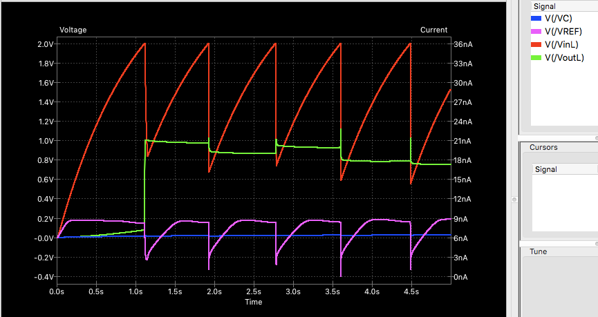
Input current I (via R1) in dependency of input voltage. I(R1) = 3V/100M = 33nA to simulate the a-Si cell.
I don't know how much current the circuit will draw in real life, but taking in account low voltage source (please note, datasheets mention 25nA as upper threshold) perhaps there are some chances to fit into the a-Si cell current budged.
-
@Mishka Thank you very much for that link. Gosh, it sure would have been awesome to have such an ultra low power wake-on radio such as that described there. Unfortunately, I'm still getting no reply to even my second email attempt at contacting the company. Maybe they'll reply later, but for now I'm going to assume they are closed for business during the Caronavirus attack.
Fortunately, Figure 5 in the paper you linked shows an equivalent transistor layout for the voltage detector. It lacks a BOM with part numbers, but I'll nonetheless take a quick run at trying to simulate it in LTSpice--maybe I'll get lucky. If you were in my shoes, exactly which simulated transistors/mosfets would you be trying?
As for alternatives to the UB20M, the nearest I could find is this:
https://www.ablic.com/en/doc/datasheet/photo_ic/S5470_E.pdf
which, admittedly, isn't as nice because it is an ultra low current detector rather than a low voltage detector. Its quiescent current is higher than the UB20m, but it appears to be still quite low in absolute terms. What the S5470 does have that the UB20M lacks though is that the s5470 is well stocked at Digikey and similar places. :)Have you run across any other parts that might fit the UB20M role?
Edit: I put Figure 5 into LTSpice. I could get it to generate the ~100mv reference voltage, but it doesn't appear to switch anything nor "detect" and then switch anything either. So, maybe there is more to the circuit that what they are showing. Given the circumstances of not being able to acquire their UB20M, it's a bit of a let down. :(
@NeverDie said in 💬 The Harvester: ultimate power supply for the Raybeacon DK:
Have you run across any other parts that might fit the UB20M role?
The UB20M is hard to beat. But there's another sub-nanoamp option: https://www.vishay.com/docs/66597/sip32431.pdf
-
@NeverDie said in 💬 The Harvester: ultimate power supply for the Raybeacon DK:
Have you run across any other parts that might fit the UB20M role?
The UB20M is hard to beat. But there's another sub-nanoamp option: https://www.vishay.com/docs/66597/sip32431.pdf
@Mishka said in 💬 The Harvester: ultimate power supply for the Raybeacon DK:
@NeverDie said in 💬 The Harvester: ultimate power supply for the Raybeacon DK:
Have you run across any other parts that might fit the UB20M role?
...But there's another sub-nanoamp option: https://www.vishay.com/docs/66597/sip32431.pdf
How would the vishay fit into it? Are you thinking you would switch it on-off using an ALD mosfet, or ...?
-
@NeverDie said in 💬 The Harvester: ultimate power supply for the Raybeacon DK:
Fortunately, Figure 5 in the paper you linked shows an equivalent transistor layout for the voltage detector. It lacks a BOM with part numbers, but I'll nonetheless take a quick run at trying to simulate it in LTSpice--maybe I'll get lucky. If you were in my shoes, exactly which simulated transistors/mosfets would you be trying?
That's true. The components selection is the hard part. I din't find anything, but the MOSFET arrays by ALD, and I see you've found them already.
It seems the most of discrete elements are tied to nanoamps and only few are diving to picoamps area. For example, the Nexperia settled it to 25 nA, as well as the TI does. But for some selected integrated circuits there are the picoamps, and some opamps may draw only femtoamps which is impressive. There is also the nice article on possible design issues - quite surprising - when building such a uber-low-power circuit - https://www.edn.com/design-femtoampere-circuits-with-low-leakage-part-one/
As for alternatives to the UB20M, the nearest I could find is this:
https://www.ablic.com/en/doc/datasheet/photo_ic/S5470_E.pdf
...
The last option I can think of would be to try these special mosfets from Advanced Linear Devices:
https://www.aldinc.com/pdf/ALD110802.pdfYeah, that's it. And the cool part is that the ALD offers 2V*200nA=400nW energy harvesters which work very similar to those we're trying to design here - http://www.aldinc.com/pdf/EH300.pdf
Unfortunately, still not sufficient to run your a-Si 80nA solar panel.
Edit: I put Figure 5 into LTSpice. I could get it to generate the ~100mv reference voltage, but it doesn't appear to switch anything nor "detect" and then switch anything either. So, maybe there is more to the circuit that what they are showing. Given the circumstances of not being able to acquire their UB20M, it's a bit of a let down. :(
It has to switch the VOUT on as soon as the VINL will be high enough to close the MN5 and pull down the VREF thus resetting the triggers and causing them to produce the VOUT.
I've put it into KiCad and immediately failed with component selection. In addition to issues with the search of a low-current MOSFETs, the ngspice has incomplete support for the modern PSPICE models. And create own models is a cumbersome task :-(
After trial and errors I've ended up switching to ngspice internal models. After some trivial tuning the circuit started to work. I've just added input (storage) capacitor and have attached a simple load (switched with an additional N-MOS) to get the simple harvester work.
On VinL≥2V input capacitor is discharged to load R2 until VinL will drop below 1V. Both voltages are configured via MOSFET gate thresholds.
For details please take a look to the eeschema file - https://drive.google.com/file/d/1O8aVj7ZzjG1TNdTJOce4i2P65X-aRLgB/view?usp=sharing.
Voltages:
Input current I (via R1) in dependency of input voltage. I(R1) = 3V/100M = 33nA to simulate the a-Si cell.
I don't know how much current the circuit will draw in real life, but taking in account low voltage source (please note, datasheets mention 25nA as upper threshold) perhaps there are some chances to fit into the a-Si cell current budged.
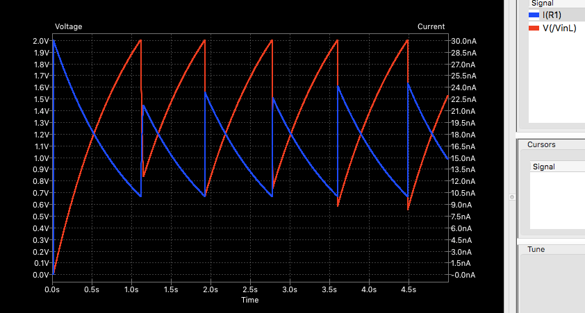
@Mishka Nice work getting it to switch. If I'm reading your graphs right, though, it look as though we're back to the land of 10+ nanoamps as opposed to the ~106 picoamps or so of the UB20M voltage detector, even though you're using the same transistor circuit as they are?
-
@Mishka Nice work getting it to switch. If I'm reading your graphs right, though, it look as though we're back to the land of 10+ nanoamps as opposed to the ~106 picoamps or so of the UB20M voltage detector, even though you're using the same transistor circuit as they are?
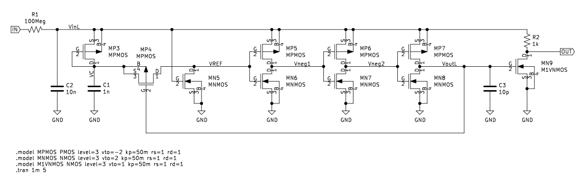
@NeverDie I've finally managed to make a readable image of the circuit. For our convenience, here it is:
The circuit self consumption is comprised of MOSFETs leakage current, and current required to charge the C1 capacitor. Regarding C1 the startup current may be arbitrary low, but sufficient to charge it eventually. After that it won't require too much to sustain the circuit. For this particular ngspce model (where MOSFETs leakage is really low) those are picoamps indeed:
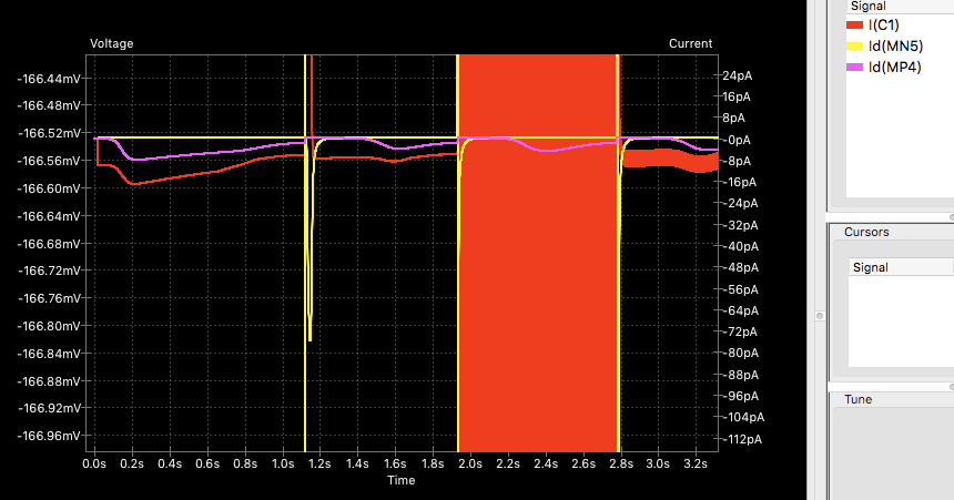
Those 30nA you've mentioned in my previous post are due to charging the C2 storage capacitor and is actually limited by R1=100MOhm resistor installed solely to emulate the weak a-Si panel. I.e. for one gigohm resistor it will not go higher than 3nA.
Of course, the model itself is far from being optimal and could be improved.