💬 The Harvester: ultimate power supply for the Raybeacon DK
-
@NeverDie said in 💬 The Harvester: ultimate power supply for the Raybeacon DK:
Unless you can think of a way to somehow roll-your-own ultra low power supervisor, I'm not aware of anything else. I suspect that maybe the Michigan team that built the Cortex M0 with the ultra tiny solar cell could easily beat both the ABLIC and Vishay supervisors--I'm still gobsmacked by what the Michigan team accomplished-- but at the moment I don't understand how to do the kind of leakage supression that's the foundation of what the Michigan team did. On my one and only attempt, after toying around with it, I was able to get one simulation that seemed to oscillate under very narrow conditions without meaningful leakage, and at first that gave me some hope. However, at the time I didn't see a way to extend that tiny, somewhat dubuious success toward anything useful. Having read the Michigan paper, can you get a leakage supression simulation working, either from their schematic or from one of the other papers? If so, that would be enormously helpful. I could post the simulation that I tried if you wanted to take a stab at it. It's not much, but pretty much anything, even an unremarkable crippled anything, is more than what typically gets published in the academic papers.
IMHO this is the promising direction to go. I haven't analyzed the circuits yet, but the super cut-off idea is dead simple - instead of grounding transistor gates, they have to be under-driven with a negative voltage. This should effectively remove free electrons from the depletion region and hence minimize drain–source leakage. Unfortunately, this requires to maintain an additional negative power source which may draw it's own current to operate. The overhead may be to expensive for a circuit with few gates, but seems well worth it for a processor core with thousands of transistors. What's good, is that this technique clearly separates optimization from the logic. In SPICE it might be easily simulated with a second voltage source, for example, at -0.1V. BTW, for the same reason the higher Vth - the lower DS leakage should be expected.
I'm thinking about building the UB40M alike circuit with any transistors. Well, the FemtoFET series is very small indeed. But size of the biggest package codename F5 is 0.73x1.49 mm which is roughly the same size as 0603 components. With proper PCB footprint soldering them should not be an issue. All in all, what must we expect from a modern high performing transistor?
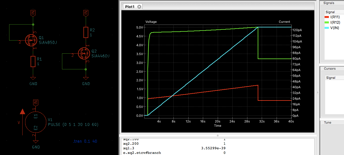
Unfortunately, my ngspice doesn't work well with the Level 7 model the TI provides. So to have anything tangible to play with I've noticed a complimentary pair from Vishay, Vth=2.5V, Vds=150V: SiA485DJ (P-channel) and SiA446DJ (N-channel). PowerPak SC-70 package also looks appealing - 2x2 mm will help save PCB space, but still not microscopic.
Unfortunately, the P-MOS has no SPICE model, damn it. I'll try to replace it with Si1411DH which parameters looks very close to the SiA485DJ, and there are SPICE models for it.
Some leakage curves for the FETs in the 0...5V range:
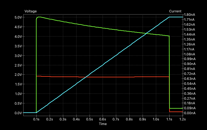
Interesting, that the faster raises the voltage - the more leakage occurs. For example, the same chart for 1s raise:
@Mishka At the "big picture" level, I like TI's approach:
http://www.freepatentsonline.com/y2019/0028089.html
because it cleanly divides the problem into separate pieces:- Generate an ultra low current. In my case I'm doing that with Gigaohm resistors, but in their case they have an ultra low current generator circuit. I like their approach better, because the current remains constant over a fairly wide range of input voltage. The ultra low current buys time because it takes capacitors longer to charge (an/or you can use smaller capacitors), and it controls leakage by brute force: no matter what, the rest of the circuit is physically unable to leak more current than it's supplied. Presumably, if I had an ultra low current generator circuit then I could delete the gigaohm resistors in my circuit du jour and use it instead. Also, if it were a constant current generator, then presumably the switching near the threshold would happen faster, because you aren't waiting on an exponential decay timeline, as is the case with charging a capacitor with just a voltage source and a resistor. Instead, the capacitor voltage would change in a linear timeline.
- Make a currenet starved Schmitt Trigger inverter. Well, that's TI's twist on the subject. I suppose the "Schmitt Trigger" part is actually optional. Fundamentally, just getting a current starved or leakage suppression inverter to work is the core of the problem. A paper I read suggests that the betas on the nmos and pmos may need to match.
- Combine #1 and #2 and, Voila, make a ring oscillator. Presumably this will be the easiest of the three steps.
-
I had a chance to try both the ABLIC faint signal detector and the Vishay load switch.
Originally I had thought the ABLIC was meant to be a current DETECTOR, but it turns out not to be so in the way that I had thought. Rather, it's more like a current SINK that will sink any and all current presented to it and that will switch if the POWER that's sunk is great than 0.7 nanoWATTS. So, the notion of putting the ABLIC between an NPN transistor and GND in my BJT oscillator circuit isn't going to work, because at that point in the circuit there's very little voltage remaining to drive the current, and hence, not enough power to turn on the ABLIC switch.
It could be made to nominally work if it's supplied with enough power (0.7nW or greater), but 0.7nW is actually quite significant in relation to my BJT oscillator circuit's power consumption. At least it's an option though.
I think the best way to run the ABLIC would be with short but infrequent pulses, because then its current drain could be amortized over the entire cycle. It would need to latch if triggered so that the detection could persist beyond just the short pulse. If the ring oscillator were also made into a charge pump, then I would guess that the the entire setup could be used to detect lower voltages. Perhaps something like:

-
I had planned to use a uCurrent Gold with a 500,000 count DMM to measure currents below 1na, but there's simply too much variation in the voltage reading depending on how close I am standing to the DUT to get meaningful measurements. The problem appears to be the multimeter test leads. Even just moving my hands near them changes the measurement. It's not that it's noisy (moving up and down and all around). Rather, it shifts around depending on where I am standing in relation to it. Do I need special test leads, or will I need to use something else (either an o-scope or a specialized circuit) to get a measurement without this problem?
Or maybe it's static electricity and I need to earth ground everything, including myself?
Edit1:
Reporting back: I put everything on an anti-static mat and earthgrounded both it and myself. That cleared up my multimeter going bonkers, at least when it wasn't connected to the DUT. Right now it appears that the Vishay load switch, or more likely my mounting of it, is what's amplifying static electricity or some other stray voltages. So, I'm going to take another pass at grounding the adapter board I soldered it to and removing residual flux to see if that helps at all. Adding a bypass cap will also likely help.I suspect that a better quality anti-static mat might be worth a try. The one I'm trying is brand new, fresh out of the box, but it doesn't have the conductive rubber like the more professional ones have. Also, the wrist strap didn't work well at all. I got better results from leaning my skin against the mat. Perhaps I need a conductive gel for the anti-static wrist strap to work better? And I don't have a conductive anti-static floor mat, so that's also a weak link in the current setup. Perhaps I should just remove myself from the equation and do the measurements remotely, via wireless link?
Edit2: I tried all of the above (short of getting proper conductive mats), and it all seemed to help, except in the case of the uCurrent Gold. Maybe because it has it's own virtual ground? In any event, I'm not confident I can get better than 1na resolution out of it if I'm physically anywhere near it. I think I would likely need more specialized instrumentation, perhaps remotely operated, to get decent sub-nanoamp measurements.
Edit3: Using a sticky gel electrode pad from a TENS on my wirst insead of an el cheapo plastic wrist strap seems to be a big improvement in terms of grounding my body. I presume it's because the TENS pad makes for a better connection (more conductive interface) between my skin/body and ground.
Edit4: I posted this picoamp uCurrent Gold problem on eevblog:
https://www.eevblog.com/forum/beginners/static-control-requirements-for-picoamp-measurements-using-ucurrent-gold/new/#new
so hopefully that will produce some informed insight/advice. -
As a ballpark, I'm starting to doubt it's worthwhile to target solar sources which produce less than 7na under dim light. Even if 100% of the current could be harvested without any declines, it would take 8 hours at a constant 7na rate to charge a 100u capacitor from 0 volts up to 2 volts. At that level, I'm sure I can get a wireless node to send or listen for enough packets to be interesting.
I'm estimating my supervisory overhead, if successful, may come out to around 1na. So, in all likelihood, the "worthwhile" lower bound for solar harvesting will be somewhere in the 1na to 7na range for a wireless node. A realistic lower bound would most likely be an even higher range to account for inevitable inefficiencies.
My keychain solar panel can produce 88na (short circuit current) under 1 lux lighting, give or take. So, when it's finally all put together, I guess the only thing that's going to vary will be just how dim it can all still function at.
On the other hand, if the light is reasonably bright, then even just a single photodiode may suffice as a worthwhile power source. In that case the entire device could, in theory, be ridiculously small.
Still, I suppose the most conservative answer comes not from how much energy is required to charge a 100u cap from 0 volts 2 volts, but rather in how much energy is required to sustain that level (while accomplishing at least some minimal amount of work) once it has been achieved. In that case, the minimum harvested energy would just be the supervisory overhead plus storage capacitor leakage plus the energy required to , say, power up an MCU and send one packet once per 24 hours. All the MCU's currently on the market that I'm aware of consume more than 7na even while turned off, so the MCU would need to be turned off by a load switch, or in some other way by the supervisor, to eliminate even that minimal level of drain.
For that reason, I tried measuring the quiescent current of the Vishay load switch using the uCurrent Gold, which is when I ran into the picoamp measurement issues. The measurements I got were all over the map, but they were all less than 1 nanoamp.
That's an outline for getting the most aggressive answer. To finish the calculation I'll need to measure the total energy consumed by a wireless MCU powerup cycle, and that will depend on the particular wireless MCU that's chosen. That in turn will inform whether sleeping the MCU will actually consume less than a full power cycle. In the case of an atmega328p and an RFM69, the combined sleep current is 200na, but that alone doesn't account for the energy expended waiting for the radio's high speed oscillator to come up to speed and its PLL to engage.
Here's a benchmark for comparison: A 5x4mm PIN diode can produce as much as 45ua at an open circuit voltage of 320mv: https://www.mouser.com/datasheet/2/427/vemd5080x01-1767531.pdf
Boosting that to 3 volts might yield 3 to 4 microamps at that higher voltage. Accumlating that electricity over time means that, at least in principle, the entire wireless node could be 5x4mm in size, or even smaller if a smaller PIN diode were used.. -
There's another class of component that might bear looking into. In December 2019 Omron released:
https://omronfs.omron.com/en_US/ecb/products/pdf/en-g3vm-21mt.pdf
which is a MOS FET Relay that, when switched off, has a maximum leakage current of 1 picoamp. This is a solid state relay, not a mechanical relay. That kind of performance comes at a cost of about $30 per device. However, maybe something not quite as state of the art would still impress at a more favorable cost? I can't say, as I haven't explored the category. I might be happy with with even 100pa leakage, especially if it were available at a much lower cost. -
The next test circuit I'll build will be this one:
On VF1 there's a nice 3 volt voltage swing. It's just a small step and will consume around 8na. Not enough current though for blinking LED's to know whether or not it's working, so I configured an MCP6022 as a voltage follower that I'll hook up to VF1 to confirm whether it's working as expected. The MCP6022 voltage follower should have an input bias of around 1pa, so it shoud not disrupt the circuit. If it shows the circuit is working as the simulator predicts it will, then I'll connect the Vishay load switch to VF1 and see if the circuit still works. If so, then the next step will be to swap the 10gohm resistors for 50gohm, and the 1gohm for 10gohm. That will take the total current drain to below 1na. If the circuit still works with the Vishay load switch connected, then bingo. If it doesn't, then I'll need some other low power way for the oscillator to drive a load.Another possibility would be to build a ring oscillator out of the Vishay load switches. I can't think of any reason why that wouldn't work, and it would kill two birds with one stone. Because it seems so promising, I may even try it before the above. The only drawback is that because of no spice model, there's no way to simulate it prior to building it.
Edit1: Here is the MCP6022 voltage follower:
I air-wired all the connections and UV-glued both the chip and the wires to the protoboard so as not to strain the DIP pins. The protoboard is supported by 1 inch nylon stand-offs. This was the first-pass. I will add some bypass capacitors to polish it off even though initial testing indicates it works well enough without them. It's a two opamp DIP. The sensed voltage (orange wire) feeds the first opamp, which then feeds the input of the second opamp via the white wire. It's the output of the second opamp (yellow wire) which you then measure with your DMM. The red wire is the supply voltage, and the black wires are GND.Edit2: The question of the moment is: how best to make the low leakage Vishay load switch into a low leakage inverter? One idea would be to have it drive a low-leakage p-channel jfet, such as perhaps the J177, which has a max cut-off voltage of 2.5v. Are there any p-channel mosfets with a lower max cut-off than that? According to the J177 datasheet, the drain cut-off current will be less than 1 nanoamp at a DS of 15 volts, so presumably much less than 1na at lower DS voltages.
Edit3: Looks as though J270 will be better: it has has a max drain cut-off voltage of 2.0v.
Edit4: Although it's an n-channel JFET, the 2n4118 sounds interesting. According to the datasheet, its typical leakage is just 0.25 picoamp at a Vgs of 20 volts: https://www.mouser.com/datasheet/2/676/jfet-2n4117-2n4118-2n4119a-interfet.r00-1649084.pdf
It also has a -1.8v cut-off voltage, so slightly better in that department. It doesn't indicate an Ids leakage current though.Maybe better is the 2N4339:
https://www.mouser.com/datasheet/2/676/jfet-2n4338-2n4339-interfet.r00-1649114.pdf
It has a cut-off voltage of just -1v, an IGSS of 100pa, and, unlike the 2n4117a, it does list its Id(off) current leakage of 50pa.Any other ideas? -
The next test circuit I'll build will be this one:
On VF1 there's a nice 3 volt voltage swing. It's just a small step and will consume around 8na. Not enough current though for blinking LED's to know whether or not it's working, so I configured an MCP6022 as a voltage follower that I'll hook up to VF1 to confirm whether it's working as expected. The MCP6022 voltage follower should have an input bias of around 1pa, so it shoud not disrupt the circuit. If it shows the circuit is working as the simulator predicts it will, then I'll connect the Vishay load switch to VF1 and see if the circuit still works. If so, then the next step will be to swap the 10gohm resistors for 50gohm, and the 1gohm for 10gohm. That will take the total current drain to below 1na. If the circuit still works with the Vishay load switch connected, then bingo. If it doesn't, then I'll need some other low power way for the oscillator to drive a load.Another possibility would be to build a ring oscillator out of the Vishay load switches. I can't think of any reason why that wouldn't work, and it would kill two birds with one stone. Because it seems so promising, I may even try it before the above. The only drawback is that because of no spice model, there's no way to simulate it prior to building it.
Edit1: Here is the MCP6022 voltage follower:
I air-wired all the connections and UV-glued both the chip and the wires to the protoboard so as not to strain the DIP pins. The protoboard is supported by 1 inch nylon stand-offs. This was the first-pass. I will add some bypass capacitors to polish it off even though initial testing indicates it works well enough without them. It's a two opamp DIP. The sensed voltage (orange wire) feeds the first opamp, which then feeds the input of the second opamp via the white wire. It's the output of the second opamp (yellow wire) which you then measure with your DMM. The red wire is the supply voltage, and the black wires are GND.Edit2: The question of the moment is: how best to make the low leakage Vishay load switch into a low leakage inverter? One idea would be to have it drive a low-leakage p-channel jfet, such as perhaps the J177, which has a max cut-off voltage of 2.5v. Are there any p-channel mosfets with a lower max cut-off than that? According to the J177 datasheet, the drain cut-off current will be less than 1 nanoamp at a DS of 15 volts, so presumably much less than 1na at lower DS voltages.
Edit3: Looks as though J270 will be better: it has has a max drain cut-off voltage of 2.0v.
Edit4: Although it's an n-channel JFET, the 2n4118 sounds interesting. According to the datasheet, its typical leakage is just 0.25 picoamp at a Vgs of 20 volts: https://www.mouser.com/datasheet/2/676/jfet-2n4117-2n4118-2n4119a-interfet.r00-1649084.pdf
It also has a -1.8v cut-off voltage, so slightly better in that department. It doesn't indicate an Ids leakage current though.Maybe better is the 2N4339:
https://www.mouser.com/datasheet/2/676/jfet-2n4338-2n4339-interfet.r00-1649114.pdf
It has a cut-off voltage of just -1v, an IGSS of 100pa, and, unlike the 2n4117a, it does list its Id(off) current leakage of 50pa.Any other ideas?Hi @NeverDie,
I also have the strong feeling that a couple of voltage detectors could make it much easier, yet – due to picoamps leakage – more effective.
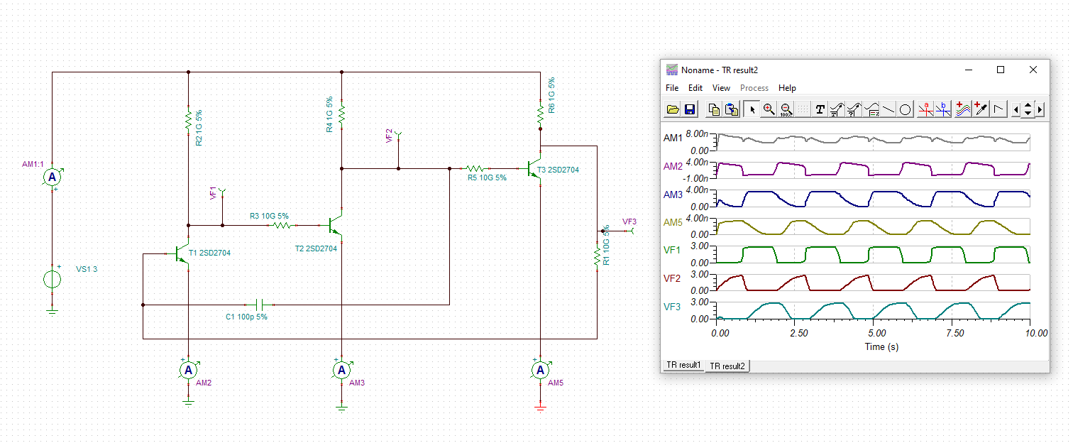
Such, in the couple of last days I've tried to reproduce the UB40M circuit with real transistors. Perhaps, when you build a die you can construct every transistor with the parameters you need, but I admit it was not a trivial task to pick anything suitable from a catalogue. I defined no strict constraints to the application, rather tried to be opportunistic and use whatever works. There were some assumptions though:
- Input voltage is defined by the solar cell and is somewhere between 2V and 3V. In the deign below it's set to 2.5V.
- The short circuit current for the cell should not extend 50 nA. I've limited it down to 25 nA with the Rcell = 2.5V/25nA = 100MΩ.
- The harvester should be able to charge 22µF storage capacitor - this capacity should be enough to send a single non-connectable BLE advertisement.
I haven't bothered to find the low leaking MOSFETs and chose something small, handy to solder, cheap, and in stock. That turns out to be power MOSFETs in PowerPAK SC-70 package from Vishay. The nomenclature is SiAxxxDJ where the xxx is what you may see in the circuitry below. For example, 421 stands for SiA421DJ.
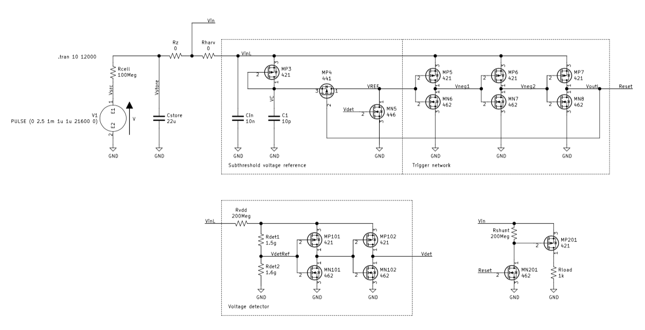
The core of the circuit is the pretty much of the UB40M reference design. The series of MP5-MP7/MN6-MN8 triggers will pull Reset line high when VREF will become low. This will happen when MN5 will pull it down, and depends on the Vdet voltage. At the same time, the MP4 will be turned off by VoutL (Reset) thus preventing VinL from being unintentionally pulled to the GND. The MP3 is used as a diode there.
I failed to create the VREF voltage in the way it was defined in the Bristol paper. With the circuit powered by the very low-power source, it suffers from transient processes a lot. To address that, I went for more complicated solution with couple of triggers controlled by Rdet1+Rdet2 divider. The divider also allows to tune the circuit to better match source and storage capacitor.
Finally, there is a 1k load attached to the Vin line. It discharges the Cstore capacitor as soon as the Reset will be set high. Upon discharge, the voltage detector will went reset the Vdet and the Cstore will be charged back.
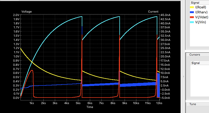
In my KiCad ngspice it looks as follows. With Vcell=2.5V, Icell=25nA the Vin oscillates between 1.4V and 1.95V. Although this is way below required 1.8V for most of sensors and MCU, raising solar cell voltage to 3.5V will shift the voltages to the usable range.
Discharge current is limited solely by the Rload=1k. At the same time, average current consumption of the harvester is about 3nA - the blue line I(Rharv). Solar cell load is below 10 nA - the yellow line I(Rcell). However, due to non-linear nature it's hard to predict how the line will look like with a real cell. Probably, it's better to simulate it with a current source, I don't know. The red line Vdet shows how the voltage detector works.
To be honest, I'm quite unhappy about the circuit.
First of all, it uses a lot of transistors, please compare this to the BJT harvesters you're working on. Also, many of them work on subthreshold voltages, and this makes it relatively hard to to tune. But worse, real devices will likely to suffer from the voltage interference which makes the whole circuit too fragile. Taking in account the money to build it (even with $0.40 per FET), it turns out the circuit shall be considered rather impractical.
:man-shrugging: -
Hi @NeverDie,
I also have the strong feeling that a couple of voltage detectors could make it much easier, yet – due to picoamps leakage – more effective.
Such, in the couple of last days I've tried to reproduce the UB40M circuit with real transistors. Perhaps, when you build a die you can construct every transistor with the parameters you need, but I admit it was not a trivial task to pick anything suitable from a catalogue. I defined no strict constraints to the application, rather tried to be opportunistic and use whatever works. There were some assumptions though:
- Input voltage is defined by the solar cell and is somewhere between 2V and 3V. In the deign below it's set to 2.5V.
- The short circuit current for the cell should not extend 50 nA. I've limited it down to 25 nA with the Rcell = 2.5V/25nA = 100MΩ.
- The harvester should be able to charge 22µF storage capacitor - this capacity should be enough to send a single non-connectable BLE advertisement.
I haven't bothered to find the low leaking MOSFETs and chose something small, handy to solder, cheap, and in stock. That turns out to be power MOSFETs in PowerPAK SC-70 package from Vishay. The nomenclature is SiAxxxDJ where the xxx is what you may see in the circuitry below. For example, 421 stands for SiA421DJ.
The core of the circuit is the pretty much of the UB40M reference design. The series of MP5-MP7/MN6-MN8 triggers will pull Reset line high when VREF will become low. This will happen when MN5 will pull it down, and depends on the Vdet voltage. At the same time, the MP4 will be turned off by VoutL (Reset) thus preventing VinL from being unintentionally pulled to the GND. The MP3 is used as a diode there.
I failed to create the VREF voltage in the way it was defined in the Bristol paper. With the circuit powered by the very low-power source, it suffers from transient processes a lot. To address that, I went for more complicated solution with couple of triggers controlled by Rdet1+Rdet2 divider. The divider also allows to tune the circuit to better match source and storage capacitor.
Finally, there is a 1k load attached to the Vin line. It discharges the Cstore capacitor as soon as the Reset will be set high. Upon discharge, the voltage detector will went reset the Vdet and the Cstore will be charged back.
In my KiCad ngspice it looks as follows. With Vcell=2.5V, Icell=25nA the Vin oscillates between 1.4V and 1.95V. Although this is way below required 1.8V for most of sensors and MCU, raising solar cell voltage to 3.5V will shift the voltages to the usable range.
Discharge current is limited solely by the Rload=1k. At the same time, average current consumption of the harvester is about 3nA - the blue line I(Rharv). Solar cell load is below 10 nA - the yellow line I(Rcell). However, due to non-linear nature it's hard to predict how the line will look like with a real cell. Probably, it's better to simulate it with a current source, I don't know. The red line Vdet shows how the voltage detector works.
To be honest, I'm quite unhappy about the circuit.
First of all, it uses a lot of transistors, please compare this to the BJT harvesters you're working on. Also, many of them work on subthreshold voltages, and this makes it relatively hard to to tune. But worse, real devices will likely to suffer from the voltage interference which makes the whole circuit too fragile. Taking in account the money to build it (even with $0.40 per FET), it turns out the circuit shall be considered rather impractical.
:man-shrugging:You may be unhappy with your circuit at the moment, but to my eyes it looks like you've got some traction and you've made a good start.
@Mishka said in 💬 The Harvester: ultimate power supply for the Raybeacon DK:
I haven't bothered to find the low leaking MOSFETs and chose something small, handy to solder, cheap, and in stock. That turns out to be power MOSFETs in PowerPAK SC-70 package from Vishay. The nomenclature is SiAxxxDJ where the xxx is what you may see in the circuitry below. For example, 421 stands for SiA421DJ.
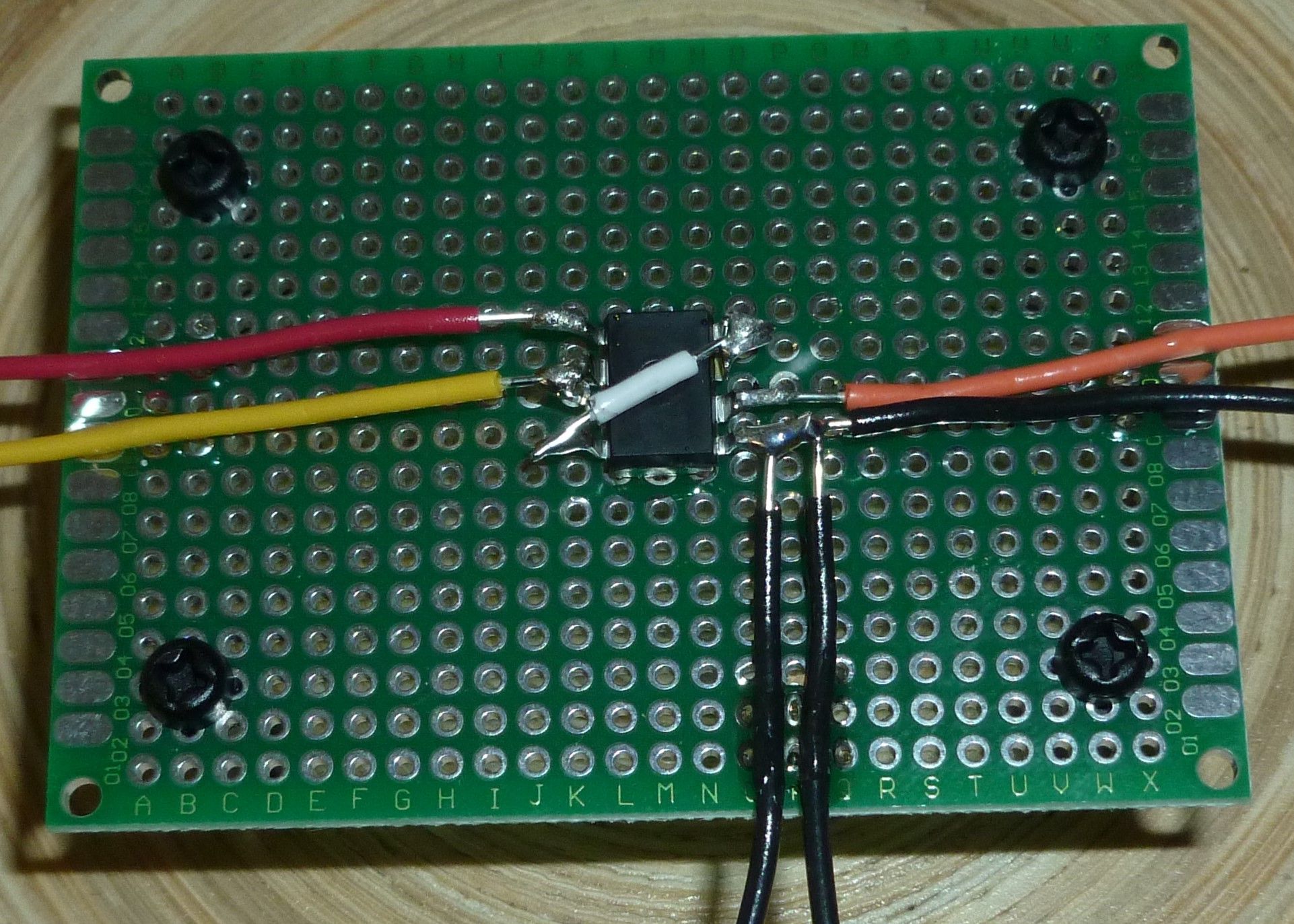
Not sure if what I'm finding out about my Vishay SiRA80DP mosfet might be similar to your Vishay mosfet, but I'll mention it anyway as a possible "heads up": I'm finding evidence of a pretty wide discrepancy between Vishay's SPICE model and what's physically true by measurement. Although I don't yet have a picoammeter (I'll be building one soon) for a more definitive test, I was able to do a relevant measurement with the voltage follower I built (see picture in previous post). The test circuit, to indirectly compare leakage of two different mosfets, was this:
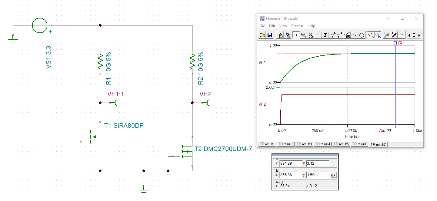
If the mosfets were ideal and there were no leakage in either mosfet, then presumably the voltage measured at VF1 and VF2 would both be 3.3v. But, of course, they're not ideal: simulation shows that VF1 would be 3.12v an VF2 would be 1.59mv. I built the circuit and the actual measurements, taken with my voltage follower and a DMM, were almost the complete opposite: VF1=280mv and VF2=3.01v. i.e. the Vishay mosfet measured as far more leaky than predicted by TINA TI spice simulation of Vishay's SPICE model, and the other N-Channel mosfet (one of two mosfets on Diodes Incorporated DMC2700UDM-7) measured as far less leaky than predicted. It's a very easy test to perform... ahem, that is, if you are in possession of a 10 gigaohm resistor and a buffer (voltage follower) with a picoamp input bias. :wink:Edit1: Come to think of it, a better way to test would be to use no resistor and just measure how much leakage there is with the gate set to GND. The leakage would likely be in the nanoamps, so it could be measured with a uCurrent Gold, or equivalent, which maybe you already have in your possession. Setting the DS voltage to whatever is listed in the datasheet for the leakage value would then give a number that can be directly compared to the leakage entries in the datasheet. Much easier and doesn't require high value resistors or exotic buffers! :grin: Obvious in retrospect. May or may not require a picoammeter, depending on the mosfet. To cover all the cases, I'll try these measurements after I build my picoammeter (soon!). I'll be building the inexpensive picoammeter designed and already vetted by an EEVBlog user named "Gyro":
https://www.eevblog.com/forum/beginners/static-control-requirements-for-picoamp-measurements-using-ucurrent-gold/msg3068708/#msg3068708
For anyone interested, you can find photos and all the details here: https://www.eevblog.com/forum/projects/picoammeter-design/msg790045/#msg790045
Rather than reduced to a nice simple PCB, the critical parts are air-wired, which is deemed the superior method according to the op-amp's datasheet. In addition, to better ensure accuracy, the DUT and all the measurement instruments should be enclosed together within conductive shielding as a countermeasure against external interference when measurements are taken. -
I tried soldering wires directly to some femtofet's, but I've concluded they either need to be locked down to a larger substrate with glue or else properly reflowed in an oven. Otherwise, they behave like super energetic tiddly-winks: even the slightest bump when attaching the first wire will make the femtofet jump great distances, most likely never to be found or seen again. :face_with_rolling_eyes: I lost 3 in a row that way, so my next attempt will use glue and very fine wire. I have an idea on how I might pre-align the wires prior to soldering, which is probably necessary in order to hand solder such a tiny thing.
My first attempt at a picoammeter is almost built. Unfortunately, it might might work well only with a DMM and not so well with an o-scope. So, I may have to build something different for that.
-
Regarding the hand soldering of itty-bitty components, this inspiring video shows it can be done:
https://www.youtube.com/watch?v=edERx4x5eY0 -
I tried soldering wires directly to some femtofet's, but I've concluded they either need to be locked down to a larger substrate with glue or else properly reflowed in an oven. Otherwise, they behave like super energetic tiddly-winks: even the slightest bump when attaching the first wire will make the femtofet jump great distances, most likely never to be found or seen again. :face_with_rolling_eyes: I lost 3 in a row that way, so my next attempt will use glue and very fine wire. I have an idea on how I might pre-align the wires prior to soldering, which is probably necessary in order to hand solder such a tiny thing.
My first attempt at a picoammeter is almost built. Unfortunately, it might might work well only with a DMM and not so well with an o-scope. So, I may have to build something different for that.
-
I have a working picoammeter now:
Because it's a very sensitive measuring instrument, I'm working out how to automate the collection of measurement data so that all measurements of a DUT can be made within a shielded secondary enclosure. -
XC6190 is a voltage detector (1.47v trigger voltage) with what it claims is just a 10na quiescent current. Sounds pretty good to me:
https://www.mouser.com/datasheet/2/760/XC6190-837296.pdf -
Here's a courtesy heads-up.
I just now stumbled across a circuit:

published here:
https://www.edn.com/solar-powered-motor-runs-on-10-na/
that allegedly can operate on as little as 10na while collecting energy, which it then uses to power a small pager motor once a threshold voltage is reached.It also has the virtue of utilizing inexpensive jelly bean parts and not relying on gigaohm resistors, which in the Dave Johnson circuit turned out to be so large that I lack the means to verify their specs through measurement after they are delivered.
This other guy instantiated the circuit as a PCB, and he made the gerber for it available as a free download: https://hackaday.io/project/159691-electron-bucket-extreme-power-management-module
If it turns out to be true that the circuit can both collect the current and trigger at a threshhold voltage all with just 10na of overhead, then on its face it sounds better than the David Johnson circuit turned out to be and possibly also better than many/most/(all?) of the commercial chips that we've reviewed on this thread if paired with an appropriate amorphous solar panel.
Edit:
But wait! There's more. There appears to exist an equivalent single chip voltage detector that also consumes a mere 10na of current: https://www.akm.com/content/dam/documents/products/power-management/power-ic-for-energy-harvesting/ap4405aen/ap4405aen-en-datasheet.pdf
It's itty bitty, so it's probably a great fit for your uber-compact design."But I want more!" I can hear you say. "I want a total step-up solution! And I want one that doesn't use a transformer!" Well, of course you do. Who wouldn't? Apparently, a 0.2v transformerless step-up solution does exist as well. I'm just not sure where. They developed it for a customer who wanted to harvest energy from... bacteria. Actually, the official term is "microbial fuel cell." The chip is the AP4470, and thankfully it can also be powered by solar, without bacteria.
https://solutions.akm.com/us/en/applications/energy-harvesting/
But can we buy it? Or is it just another inaccessible research project? I don't yet know. Can you read Japanese? The trail of bread crumbs written in English seems to run cold after the above link, but there's more about it that's written in Japanese. Argh. -
Gah! I've lost the ball :disappointed:
No progress on discrete harvester, sorry. Also, the PV panels I got earlier were shelved until better times.
I still monitor a couple of the SPV1050 devices though. They're running from various PV panels that I switch from time to time. The load is an nRF52833 beacon and sometimes an IMU broadcasting every one second at 0dBm to 8dBm and reporting voltage of attached ML2032 battery to my phone.
My experience is that a tiny PV panel cannot sustain the device working online. By online I mean that both the device and the harvester power consumption exceeds the panel capabilities, so the battery slowly decays. A bigger panel can address the issue. I still unsure how much we will win if a more efficient online harvester like AEM10941 or even more efficient R1800K will be used. A batch harvester is definitely the way to go.
But how about you? Have you had a chance to build anything yet?
-
Gah! I've lost the ball :disappointed:
No progress on discrete harvester, sorry. Also, the PV panels I got earlier were shelved until better times.
I still monitor a couple of the SPV1050 devices though. They're running from various PV panels that I switch from time to time. The load is an nRF52833 beacon and sometimes an IMU broadcasting every one second at 0dBm to 8dBm and reporting voltage of attached ML2032 battery to my phone.
My experience is that a tiny PV panel cannot sustain the device working online. By online I mean that both the device and the harvester power consumption exceeds the panel capabilities, so the battery slowly decays. A bigger panel can address the issue. I still unsure how much we will win if a more efficient online harvester like AEM10941 or even more efficient R1800K will be used. A batch harvester is definitely the way to go.
But how about you? Have you had a chance to build anything yet?
@Mishka Nice to hear from you again!
When you left I decided to take a break from solar, and so I shifted my attention back to PCB milling, to take advantage of some technological progress now at fruition which resulted in inexpensive, high precision magnetic encoders that have since made cheap closed-loop stepper drivers possible.
As for solar, not sure if you caught it in the news, but worthy of note was the breakthrough announced a few months ago of 6-layer solar cells capable of 39.2% efficiency at 1 sun illumination. For solar PV, that's a monumental breakthrough. The work was done at NREL. So, although that's a very recent breakthrough and not something we can yet buy, I do think we'll be seeing more efficient than usual solar cells within a year that will be hybrid silicon and perovskite, and those will have better efficiencies than what's available now. IIRC, Oxford PV plans to launch production of 400w solar panels at year end, and those will be things that anyone can buy, and so the solar cells in them should be available as well.
-
@Mishka Nice to hear from you again!
When you left I decided to take a break from solar, and so I shifted my attention back to PCB milling, to take advantage of some technological progress now at fruition which resulted in inexpensive, high precision magnetic encoders that have since made cheap closed-loop stepper drivers possible.
As for solar, not sure if you caught it in the news, but worthy of note was the breakthrough announced a few months ago of 6-layer solar cells capable of 39.2% efficiency at 1 sun illumination. For solar PV, that's a monumental breakthrough. The work was done at NREL. So, although that's a very recent breakthrough and not something we can yet buy, I do think we'll be seeing more efficient than usual solar cells within a year that will be hybrid silicon and perovskite, and those will have better efficiencies than what's available now. IIRC, Oxford PV plans to launch production of 400w solar panels at year end, and those will be things that anyone can buy, and so the solar cells in them should be available as well.
Hi @NeverDie,
The 39% is a HUGE!
I think there is must some fundamental limit on how much we can get from these oscillations of the, well, Ether. Or is it the quantum vacuum? Or the strings? Well, the very last name to this kind of shit is the time crystals. And, no matter what the name is, the shit can oscillate, and these oscillations are the essence of the energy. So, while currently most of electronic devices employ electrons as drivers, I'm wondering would it be possible to build an electron-less system where the oscillations (aka waves) may be passed through a number of transformations, and this will bring us to some useful things.
Actually, there is RF and optics which works exactly like that. There is also a number of RF harvesters to collect the energy, but the energy is used mostly to push electrons forward, i.e. produce direct current. That's understandable - most of devices are DC. But creating some kind of a microwave transistor would be just rad.
-
@Mishka Nice to hear from you again!
When you left I decided to take a break from solar, and so I shifted my attention back to PCB milling, to take advantage of some technological progress now at fruition which resulted in inexpensive, high precision magnetic encoders that have since made cheap closed-loop stepper drivers possible.
As for solar, not sure if you caught it in the news, but worthy of note was the breakthrough announced a few months ago of 6-layer solar cells capable of 39.2% efficiency at 1 sun illumination. For solar PV, that's a monumental breakthrough. The work was done at NREL. So, although that's a very recent breakthrough and not something we can yet buy, I do think we'll be seeing more efficient than usual solar cells within a year that will be hybrid silicon and perovskite, and those will have better efficiencies than what's available now. IIRC, Oxford PV plans to launch production of 400w solar panels at year end, and those will be things that anyone can buy, and so the solar cells in them should be available as well.
Regarding the PCB milling, I found myself thinking fairly often about full-cycle manufacturing too :-)
I usually do small boards, up to 4x4 inch. For this size it should be possible to build an affordable, but highly capable machine. Some thoughts on it:
-
High precision. The machine must be able to cut tracks and pads as thin as 6 mils (0.15 mm), but 5 mils would be really nice to achieve. Because of this I'm more inclined to laser cutting. On a milling machine 6 mil gaps between tracks will be hard to do. Another advantage of laser cutting is that it won't tear tiny tracks off the board. Perhaps, even a copper foil can be laser cut. But there's also a spoon of tar: the copper is known to be very reflective and imposes higher requirements to the laser cutter - the price may increase. Another thing to note is that the laser may be not so good at removing large surface areas.
-
Kapton tape for solder mask. For sticky mask to apply, I'm also thinking about some kind of a pallet - this would allow to use cheap polyimide tapes from eBay. Alternatively, non-sticky masks can be laminated. Laminated masks will stick stronger and can be two sided - think of it as about three and more layers. Again, laser cutting is preferred here.
-
Engraving of the silk layer. Laser could be also used for high-res silk layer over the kapton tape. With laser used, the difference in distances from the head to surface because of the copper layer is not an issue. Engraving on both copper and substrate is also possible.
-
Interchangeable heads? Probably, no. The cost of the working head, either laser or milling, will likely dominate over the cost of other components - the machine is small. Seems it's more reasonable to have different machines.
-
Assembly machine. This would be my favorite, but first things first.
-
-
Regarding the PCB milling, I found myself thinking fairly often about full-cycle manufacturing too :-)
I usually do small boards, up to 4x4 inch. For this size it should be possible to build an affordable, but highly capable machine. Some thoughts on it:
-
High precision. The machine must be able to cut tracks and pads as thin as 6 mils (0.15 mm), but 5 mils would be really nice to achieve. Because of this I'm more inclined to laser cutting. On a milling machine 6 mil gaps between tracks will be hard to do. Another advantage of laser cutting is that it won't tear tiny tracks off the board. Perhaps, even a copper foil can be laser cut. But there's also a spoon of tar: the copper is known to be very reflective and imposes higher requirements to the laser cutter - the price may increase. Another thing to note is that the laser may be not so good at removing large surface areas.
-
Kapton tape for solder mask. For sticky mask to apply, I'm also thinking about some kind of a pallet - this would allow to use cheap polyimide tapes from eBay. Alternatively, non-sticky masks can be laminated. Laminated masks will stick stronger and can be two sided - think of it as about three and more layers. Again, laser cutting is preferred here.
-
Engraving of the silk layer. Laser could be also used for high-res silk layer over the kapton tape. With laser used, the difference in distances from the head to surface because of the copper layer is not an issue. Engraving on both copper and substrate is also possible.
-
Interchangeable heads? Probably, no. The cost of the working head, either laser or milling, will likely dominate over the cost of other components - the machine is small. Seems it's more reasonable to have different machines.
-
Assembly machine. This would be my favorite, but first things first.
@Mishka I wouldn't say 6 mil is easy to achieve, but some people claim they can get it on even a sub $200 machine. That was the premise for this other thread that started here: https://forum.mysensors.org/topic/7836/what-did-you-build-today-pictures/161 and then became its own thread here: https://forum.mysensors.org/topic/8735/cnc-pcb-milling
I think for just about everything I do though being able to etch at a 0.4mm lead pitch (that's 0.4mm center to center on the pads) is good enough, and that's a lot easier to achieve. For instance, that's the pitch on an SPV1050 or an nRF52832.
There is industrial equipment that can etch copper PCB directly using a laser, but it must be pricey because I have not read of any hobbyists using it. It would likely require a fiber laser.
-
-
Regarding the PCB milling, I found myself thinking fairly often about full-cycle manufacturing too :-)
I usually do small boards, up to 4x4 inch. For this size it should be possible to build an affordable, but highly capable machine. Some thoughts on it:
-
High precision. The machine must be able to cut tracks and pads as thin as 6 mils (0.15 mm), but 5 mils would be really nice to achieve. Because of this I'm more inclined to laser cutting. On a milling machine 6 mil gaps between tracks will be hard to do. Another advantage of laser cutting is that it won't tear tiny tracks off the board. Perhaps, even a copper foil can be laser cut. But there's also a spoon of tar: the copper is known to be very reflective and imposes higher requirements to the laser cutter - the price may increase. Another thing to note is that the laser may be not so good at removing large surface areas.
-
Kapton tape for solder mask. For sticky mask to apply, I'm also thinking about some kind of a pallet - this would allow to use cheap polyimide tapes from eBay. Alternatively, non-sticky masks can be laminated. Laminated masks will stick stronger and can be two sided - think of it as about three and more layers. Again, laser cutting is preferred here.
-
Engraving of the silk layer. Laser could be also used for high-res silk layer over the kapton tape. With laser used, the difference in distances from the head to surface because of the copper layer is not an issue. Engraving on both copper and substrate is also possible.
-
Interchangeable heads? Probably, no. The cost of the working head, either laser or milling, will likely dominate over the cost of other components - the machine is small. Seems it's more reasonable to have different machines.
-
Assembly machine. This would be my favorite, but first things first.
@Mishka On the other hand, as I just posted on the CNC thread, using a regular etching laser to remove black solder mask above copper pads might be an awesome solution: https://forum.mysensors.org/topic/8735/cnc-pcb-milling/801
At least notionally, it sounds more bullet proof than using a spring bit to grind off the solder mask in those locations without damaging the copper underneath. Maybe even a lower power etching laser (relatively speaking) would suffice for doing it, as long as the beam spot was sufficiently small and sharply defined. -
Hello! It looks like you're interested in this conversation, but you don't have an account yet.
Getting fed up of having to scroll through the same posts each visit? When you register for an account, you'll always come back to exactly where you were before, and choose to be notified of new replies (either via email, or push notification). You'll also be able to save bookmarks and upvote posts to show your appreciation to other community members.
With your input, this post could be even better 💗
Register Login