In wall light switch node - Custom PCB
-
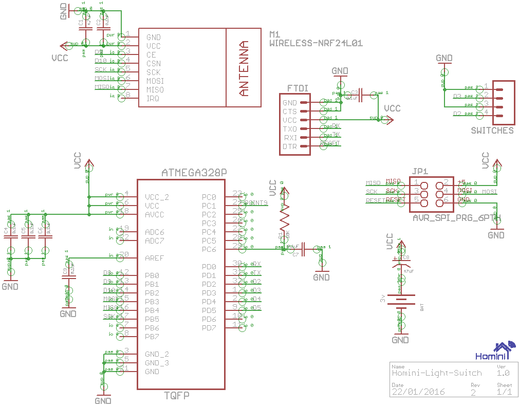
I'm seeking external help from a electronic forum. Someone has suggested that my 0.1uF caps could be too far away from the micro-controller itself. We're talking around 13-15mm away from the chip. What're you thoughts, would you say that is too far away from the chip?
-
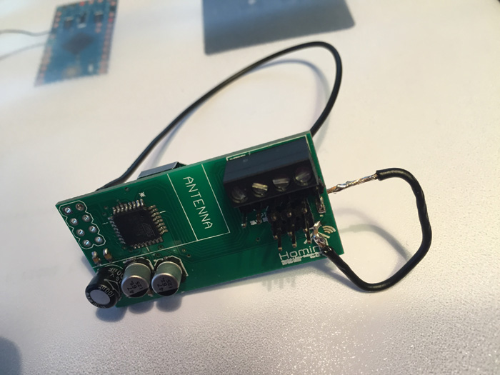
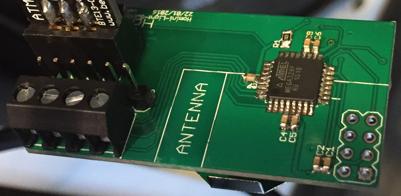
With a little open-heart surgery, the board becomes alive! While I'm yet to actually burn any bootloader to the uC itself, I have no got the circuitry working.
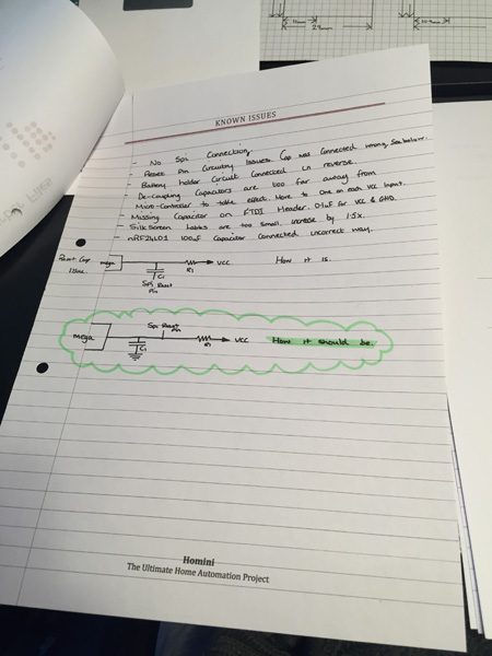
The known issues:
- Capacitor on the SPI Header was incorrectly connected. I had wired it like a resistor/diode.
- The VCC line from the SPI was connected to the uC through the resistor of the RESET circuit.
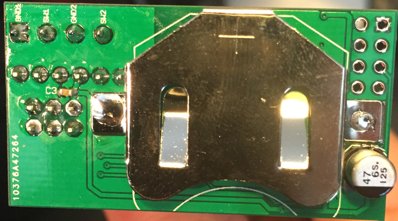
- Battery holder is connected in reverse.
I have attached images for anyone interested in following this project with actual pictures of the progression through the revisions of this node. I have now made some alterations in my documentations regarding Rev1, listed the known issues and made some possible improvements:
- Remove one 47uF capacitor.
- Move the 47uF capacitor closer to battery terminal, and have all power traces coming through that capacitor, reducing the chance of the battery being drained through large spikes in draw.
- Add capacitor to FTDI VCC to stop spikes when connecting programming board.
- Increase silkscreen labels for document data such as pinouts and node info.
- Remove the 100uF capacitor on the nRF24l01+, add a 4.7uF footprint and 0.1uF footprint. Only populate if needed.
- Turn around the switch terminals, room should allow this.
- Bring the 0.1uF capacitors closer to the VCC inputs on the uC.
This week I will be aiming to get the designs and re-routes for Rev2 sorted out, and then get them ordered, with express shipping this time hopefully. The 3 weeks of waiting killed me!
Please give your feedback, if you have any.
-
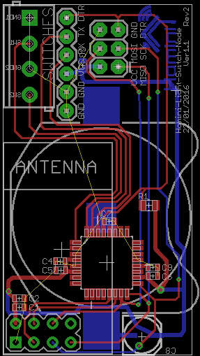
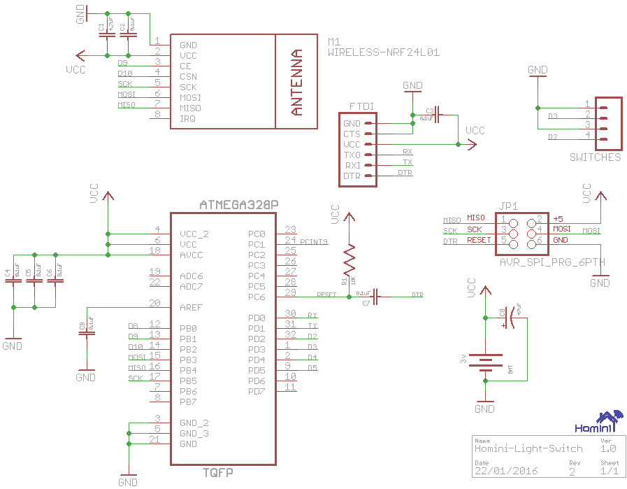
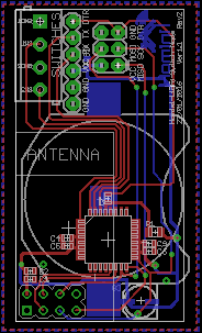
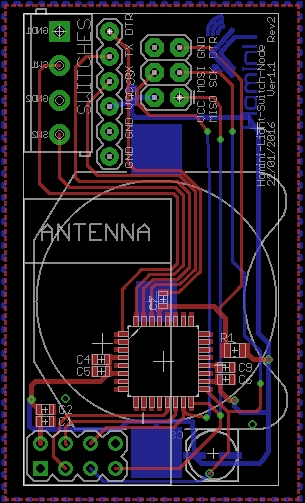
I would like to ask if someone could just double check my Schematic and Board layout for me, just as a second pair of eyes before i send the gerber files over to ITead.cc in the morning. I'm pretty sure everything is as it should be, but would like a second pair of eyes to give it a scan over.
Can't wait to get Rev2 up and running to deliver the upgrades that have been made!
Thank you in advance :)
-
I would like to ask if someone could just double check my Schematic and Board layout for me, just as a second pair of eyes before i send the gerber files over to ITead.cc in the morning. I'm pretty sure everything is as it should be, but would like a second pair of eyes to give it a scan over.
Can't wait to get Rev2 up and running to deliver the upgrades that have been made!
Thank you in advance :)
@samuel235 Look again at your Reset-Dtr net wiring compared to example and reference. Also C8 is probably ment to be in parallell with the battery.
-
@samuel235 Look again at your Reset-Dtr net wiring compared to example and reference. Also C8 is probably ment to be in parallell with the battery.
-
@samuel235 Look again at your Reset-Dtr net wiring compared to example and reference. Also C8 is probably ment to be in parallell with the battery.
@m26872 - I just have to connect the right side (positive connection) to the batt + right?
Then for the reset line, i've been having some horrible issues with understanding the connection for this and i genuinly thought i had it here with this Rev. I will study that and take a look soon as i get home today.
-
@samuel235 Look again at your Reset-Dtr net wiring compared to example and reference. Also C8 is probably ment to be in parallell with the battery.
@m26872 said:
@samuel235 Look again at your Reset-Dtr net wiring compared to example and reference.
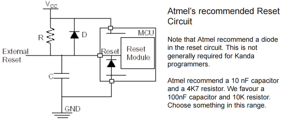
I'm sorry @m26872, however i feel that my reset line is connected correctly. I have used Atmel's recommendation to verify this and everything is exactly the same as they suggest to use apart from the fact i do not have a diode in there, which they recommend.
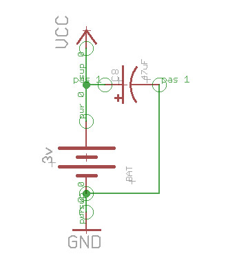
Also C8 is probably meant to be in parallel with the battery.
I have the negative connection made to the GND plane, then the positive receives its power from the BATT and then out to the various components now.
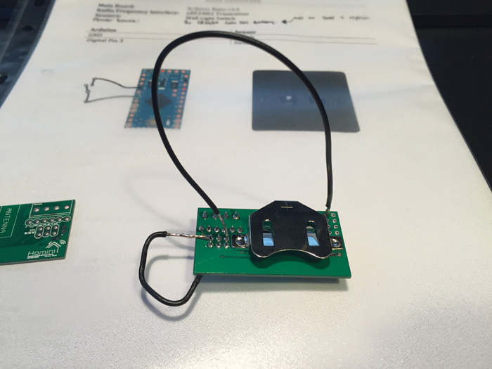
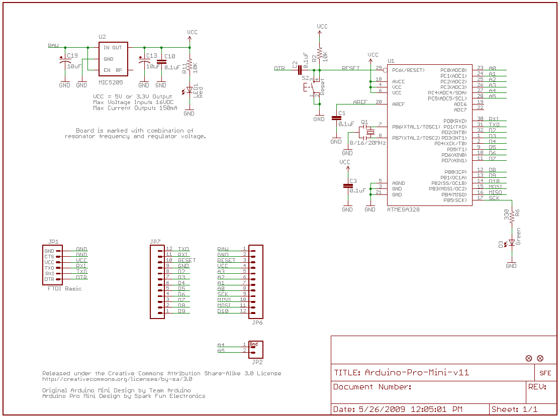
Below is 3 images, one for the modified BATT & C8 connection, one for the recommended reset circuit from Atmel, and the other is my actual reset circuit.
C8 & BATT
Atmel's recommendation for reset circuit
My Actual reset circuit
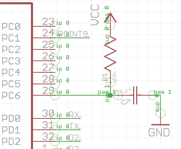
Please could you inform me where I am going wrong with the reset pin because I simply can't see anything to my knowledge.
-
I think you may add some net labels at RST, DTR. So it is less ambiguous to read ;)
Here a basic sparkfun arduino mini schematic so you can check :)
https://cdn.sparkfun.com/assets/0/7/5/5/1/51eec304ce395f104c000000.png -
I think you may add some net labels at RST, DTR. So it is less ambiguous to read ;)
Here a basic sparkfun arduino mini schematic so you can check :)
https://cdn.sparkfun.com/assets/0/7/5/5/1/51eec304ce395f104c000000.png@scalz - Labels have been added to make it easier to understand.
However, this is exactly how I wired Rev1, it didn't work until I hacked together the reset pin. I'm getting even more confused at to why my Rev1 didn't work now, I thought that by bypassing/altering the connections with some wires and it working would indicate that I had wired Rev1 incorrectly, I used the link you sent to me as reference while I was making Rev1.
However, i have done as you have suggested and attached images below. I've also attached my eagle files in case you wanted to trace any routes you can't see clearly on the images.
-
Looks good now except that AVR ISP (JP1) pin 5 should connect straight to RESET and not to DTR.
-
Looks good now except that AVR ISP (JP1) pin 5 should connect straight to RESET and not to DTR.
-
@m26872 - Does the FTDI need to go to RESET or DTR? I'm feeling DTR because all the FTDI programmers i'm using is labeled with DTR and not RESET, am i correct in assuming this?
@samuel235 Yes.
-
@samuel235 Yes.
@m26872 - Perfect. Thank you for your assistance, I really appreciate it! I'll get these ordered tonight hopefully and then keep looking at the circuitry for my RESET and DTR line to memorize it and work out why its so hard to get into my brain xD.
Just one last confirm, since I'm not that confident with myself at the moment regarding this RESET line, if you don't mind.
-
@m26872 - Perfect. Thank you for your assistance, I really appreciate it! I'll get these ordered tonight hopefully and then keep looking at the circuitry for my RESET and DTR line to memorize it and work out why its so hard to get into my brain xD.
Just one last confirm, since I'm not that confident with myself at the moment regarding this RESET line, if you don't mind.
@samuel235 Reset and Dtr routing looks correct, but you still have DTR silkscreen label next to AVR ISP.
-
@samuel235 Reset and Dtr routing looks correct, but you still have DTR silkscreen label next to AVR ISP.
@m26872 said:
@samuel235 Reset and Dtr routing looks correct, but you still have DTR silkscreen label next to AVR ISP.
Indeed I do, the board itself isn't finished yet, I just wanted you to clarify the wiring was correct. Time to tidy it up, finish the annotating and get it finalized. However, thank you for pointing it out to me (Shows you're actually paying some attention to this). Thank you, yet again. The level of support and time you dedicate to helping others on here is outstanding. It is most certainly noticed!
-
@m26872 said:
@samuel235 Reset and Dtr routing looks correct, but you still have DTR silkscreen label next to AVR ISP.
Indeed I do, the board itself isn't finished yet, I just wanted you to clarify the wiring was correct. Time to tidy it up, finish the annotating and get it finalized. However, thank you for pointing it out to me (Shows you're actually paying some attention to this). Thank you, yet again. The level of support and time you dedicate to helping others on here is outstanding. It is most certainly noticed!
@samuel235 You're very welcome. We'll all benefit when you succeed.
-
UPDATE!
Revision 2 boards have now been submitted for manufacturing. Standard shipping used, so expecting within the next 23 days. This is going to pain me!
On the side note, I've enrolled for Open University and will be studying now for around 4 years. I'm doing a Computing and IT degree to follow on from my existing IT Qualifications (Microsoft and CompTIA). I do hope to incorperate this community and the projects i take on with you guys into my studying. I also do not expect this to effect the time and effort I'm able to spend with you guys here and developing our projects together.
I will update you ASAP, when these boards get here :)
-
great :)
-
I will upload this device to Openhardware.io as soon as i have it built up and the basic functionality working. Hopefully then it will become much easier for the starting MySensor budding builders to understand and follow. I may do a 'basic build instructions' that can be followed on how to get this working, including putting the hardware together.
-
Board Revision2 got delivered today and obviously i set about populating the board instantly!
I have the board all completed and now I'm attempting to burn the bootloader on. Before i go ahead and screw my IC up (I read if you use the wrong fuse reading for the timing of the clock you can't Re-burn anything else to it) i would like some advice. I've detected the current/pre-set fuse readings through AVRDUDESS using a clock speed of 93.75KHz, so i know the connection between my computer and the board is working. The readings for the fuses are below:
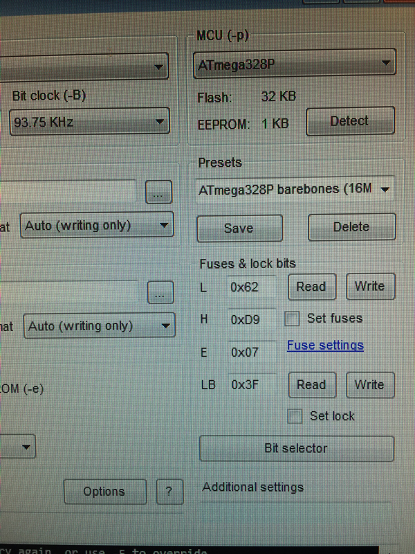
I'm currently using the fuse calculator here to workout the fuses needed. I'm also looking at Maniac's blog post here as he made a very low power module. The only thing i would question about his version/board is that his brownout is set to 2.7v. I've checked the nRF module and the lowest voltage it can go is 1.9, so maybe i should bring the BoD reading down even more or even disable it all together (I plan on reading the battery voltage from this module anyway).
The below settings for the fuses are my own workings out with the fuse calculator linked above, I'm doubting myself here, i'm in territory that i'm not comfortable with so I'm more than likely making a mistake here but what do you think? The BoD is set to 1.8 here:
Low: 0x62 | High: 0xD9 | Extended: 0xFE
Once i have confirmed a fuse setting, Do I edit them into the board.txt config of Maniac's blog post or do I use that of @tekka's?

Hello! It looks like you're interested in this conversation, but you don't have an account yet.
Getting fed up of having to scroll through the same posts each visit? When you register for an account, you'll always come back to exactly where you were before, and choose to be notified of new replies (either via email, or push notification). You'll also be able to save bookmarks and upvote posts to show your appreciation to other community members.
With your input, this post could be even better 💗
Register Login