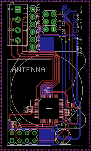
In wall light switch node - Custom PCB


  • Hardware Contributor

    @GertSanders Ahh okay, that makes complete sense now. So the default is set to Width: 10mil, Drill: 20mil, Clearance: 10mil. ITead specify Width: 8mil, Drill: 0.3mm, Clearance: 8mil, I took these figures from here.

    So I am safe to change my net classes to those of the board house to run the checks and then revert them back once i generate my gerber files? Or have i miss understood?


  • Hardware Contributor

    @samuel235 You can change the defaults to the values of the boardhouse and leave it at that. When generating the GERBER files, the DRU or net class values are no longer important. You only need the values when checking against design rules.


  • Hardware Contributor

    @GertSanders said:

    @samuel235 You can change the defaults to the values of the boardhouse and leave it at that. When generating the GERBER files, the DRU or net class values are no longer important. You only need the values when checking against design rules.

    Awesome! I shall get it checked and posted here in a minute and hopefully I'll get it ordered tonight 🙂


  • Hardware Contributor

    And the final designs are shown below. As you can see the one on the left is without the ground planes and the one on the right is with them. If anything is jumping out in terms of errors or discrepancies, please don't hold back, let me know 😉

    Brd4.jpg


  • Hardware Contributor

    UPDATE!

    Just a little update to keep you all posted; I have sent my Gerber files off, they have been confirmed to be of the correct format and my boards are now being produced. I ordered the parts last night, enough for backups/errors, soon as everything arrives i will get this made up and give you another update on the situation of the board. The only thing i wasn't comfortable with was the price of the screw terminal and the fact i used a through hole capacitor for the 100uF (C7). The next revision of the board i will be using a surface mount 100uF capacitor for this, now i managed to find it. The terminal for the switches, I'm looking at maybe having a crimped push connector on the switch that just slots onto some sort of header pin on the board instead of a screw terminal.

    Either way, Homini Light Switch Node Version 1.1 Revision 1 is on its way!


  • Hardware Contributor

    I have just received confirmation that the board house has released the PCB's. Lets see how long these take to get here! Itching to get this module on the move again. I will be back soon as they get here, don't go anywhere!


  • Hardware Contributor

    UPDATE!

    I have just received all components for the boards, we're just waiting on the boards themselves to arrive from ITead Studios.

    Time to get this project moving!


  • Hardware Contributor

    While waiting for my boards to arrive i decided to create a housing for my gateway including flashing status LEDs. Its in no means a finished product, but i feel its enough to house the gateway components while i'm building my network to save any incidents destroying the parts. Within the next few days i will get a guide up with images and maybe a video of the LEDs and their function up on a hardware guide topic. image.jpg


  • Hardware Contributor

    So then, we have another update!

    UPDATE!

    The boards ave arrived safe and sound, i have populated one of them with everything apart from the nRF module. So, its time to get the bootloader burnt. This is the daunting task for me, i have no idea what i am doing here, so if you guys feel like you could give me some helpful pointers in the right direction I would really appreciate all the help you can offer.IMG_7098.JPG IMG_7099.JPG


  • Hardware Contributor

    Hi! Depending on which bootloader you want, but why not go with the MySensors with OTA updates by tekka?
    http://forum.mysensors.org/topic/838/windows-gui-controller-for-mysensors/75

    If you want the original arduino bootloader: https://www.arduino.cc/en/Hacking/Bootloader?from=Tutorial.Bootloader


  • Hardware Contributor

    @sundberg84 - I was reading that exact post from tekka as you posted this. However, i'm probing around on my board and found for some reason my 3v line is 0.24v. So I have to do some investigation work on that this morning. Hoping the bootloader will be a piece of cake once the hardware is working as should be.


  • Hardware Contributor

    @sundberg84 So i have my hardware issue corrected now. Am i reading Tekka's instructions correctly, this new board is to be connected through serial to my gateway and then programmed essentially by the gateway through MYSController which is connected to my gateway via ethernet? Does that sound correct?


  • Hardware Contributor

    No, i would recommend you have a look at some youtube tutorials. Im not familiar with programming through the ISP headers which i think you should do. I use a seperate arudino uno as ISP programmer.


  • Hardware Contributor

    @samuel235: cool. happy for you.

    first you need to burn the bootlader in your atmel 328p. When it comes as ic-only, factory setting is 1mhz internal rc. and there is no bootloader yet. So you can't use ftdi at this moment, nor ota. So you need to burn the bootloader with avrspi. Like @sundberg84 said you can use the "arduino uno as isp programmer" method if you have an uno..On my side, I don't use this method, I prefer to use an usbasp. But both method works well.
    When burning bootloader, you will need to set fuses too, corrsponding to the bootloader.

    Sorry, I have not much time to make an howto, just point you in some direction..i hope it helps a little bit.

    Edit: you can find some howto here http://www.gammon.com.au/breadboard


  • Hardware Contributor

    @scalz I'm using a USBasp programmer, however i think i may have an issue with my reset pin. I have continuity on every other ISP header pin and the associated pin on the ATMega but not the reset pin. Is this normal, should i be seeing continuity between ISP RESET and pin 29 on the ATMega?


  • Hardware Contributor

    I think you should have continuity between avrspi connector RST pin and your atmega RST pin...don't see why not. Have you checked your routing? I think so...Maybe a bad solder on this pin???


  • Hardware Contributor

    @scalz I may have found the problem, i have just completed a x25 magnification inspection on the boards and every board has atleast one filled VIA. I'm going to get a makeshift jumper in place on this board and test for continuity again.

    I get continuity from the pin to the one side of the capacitor but nothing from the MEGA to the pin, it feels like the capacitor is stopping it coming through...


  • Hardware Contributor

    oki, so if continuity between rst atmega and one side of capacitor (dtr ftdi capacitor, right?) it should be ok. The capa is for dtr of ftdi (it is a trick for resetting atmega from ide when you want to upload).
    Is your schematic updated on your first post? I don't see a 10k resistor pullup for rst...you need it to keep rst line to 1 and then when you push a rst button, or want to reprogram it by ftdi or avrspi, it will go to low/0 briefly to tell the mcu to reset.
    if not done, try to connect a 10k res between your rst pin and vcc


  • Hardware Contributor

    @scalz I have just uploaded a zip file with my .brd and .sch files. Sorry, forgot to update those


  • Hardware Contributor

    oki seems good. so I imagine you have continuity between rst atmega/one side of the 10k res. so what is your problem to program it?
    when programming with avrspi, be careful with the fuses, especially for clock freq. For instance, if you set the clock fuse for external crystal and you have no onboard, then you could have some problem to re-set the fuse to internal clock as at this moment, the mcu will wait for an external clock. I am not sure as I have never tested this, and I am careful when I set the fuses, but in eventuality I am tired and make a mistake, I like to put a crystal footprint. but sometimes, you have not enough room unfortunately.


  • Hardware Contributor

    @scalz I get continuity from the ATMega to the resistor and one side of the cap. But its not flowing through the cap. So you think i should be good to program from there? I try to test a connection to the board with AVRDude, by running "C:>avrdude -c usbasp -p m328p" and then i get

    avrdude: error: programm enable: target doesn't answer. 1
    avrdude: initialization failed, rc=1
             Double check connections and try again, or use -P to override this check.
    
    avrdude done. Thank you.
    

  • Hardware Contributor

    yep, for capa it is not a problem. so it should work, but your log seems indicating a connection problem...but I don't see it 😳 and I don't have much time for the moment...sorry.
    for avrdude cli, I can't help you as I use avrdudess. no need of cli, a little bit easier.


  • Hardware Contributor

    @scalz While feeding the board 3v, every part of the VCC line from the battery to the chip is perfect, however if i test a VCC pin and a GND pin on the chip, it reads 0.06. Would this be an issue?

    Maybe i should have connected all of the vcc's together or even pulled another to the battery directly, the only vcc connection going to the mega is from the DTR/RESET pin on the SPI header, that flows through the resistor to the mega. Is this an incorrect wiring issue?


  • Hardware Contributor

    Okay, so for some reason i seem to have not connected all the VCC's together unfortunately, i personally believe this is where my issue lies. If anyone feels differently, please shout out and let me know.


  • Hardware Contributor

    @samuel235: i have just looked briefly to your .brd this time 😉 .So, for your next rev:

    • you have airwire. You have to have no airwire at all or you must know what you do. Here you have an airwire on your batt which is not connected to mcu. So of course it can't work. You can fix this by soldering a wire between Batt_vcc and radio_vcc. it should work. Sometimes, when board is complex, you can't see everything, and sometimes airwire are micro..in eagle you can see these : File menu/run ulp/ and launch zoom_unrooted.ulp. It will highlight these.
    • decoupling capa, which are not always mandatory, but for a mcu I would say yes, needs to be placed near the concerned chip. Your board is small so it should work. but it's something to know.
    • for vcc, power line/rails, you are using 12mil (trace width I usually use mils unit as I am not familiar to inch! I'm french lol). I think it is rather small...For signals, it's ok. But for power, hum..I prefer not to go under 16mil and it's my limit. I like 20/24 or 32mils, all depends of the current.

    As you can see, pcb design is a whole science! I would advise you to persevere, you will find very good starter howto for pcb designing at sparkfun. they rocks! adafruit too. It's like kung-fu, I like to say : the path/road is long 😉 but finally it's very rewarding, yeah 😄


  • Hardware Contributor

    @scalz - While you were away i noticed about the VCC line not getting to the Mega, so i soldered a wire from batt + to the nRF vcc, like you just confirmed.

    I would too prefer the traces to be bigger, however I routed them with a bigger size but i couldn't route the board completely. So i chose to bring the size down hoping to get away with it.

    So, i have made the connection with the additional wire and I'm still unable to get a test communication connection to the board through USBasp. I thought maybe its going a little too quickly for the board and so i decided to use a slower SCK speed, dropped it really low, still nothing.


  • Hardware Contributor

    arf..and now what's your vcc voltage?
    if I have an idea, I'll tell you


  • Hardware Contributor

    @scalz I'm sorry, you have confused me with arf, what does arf mean? Is it some 'slang' word? xD - My vcc voltage is 3v from a battery, if i let the USBasp power it, i set it to 3v which comes out at 3v3.


  • Hardware Contributor

    ahah. it was an onomatopia? a sort of "argh" or "gloups". I don't know how to translate it lol!
    for your vcc problem (seems now you have a true one), there is of course an answer but I have no idea for the moment...like I said if I have one I will tell you. I will try to re-look at your eagle files maybe tonight...


  • Hardware Contributor

    @scalz Ahh okay, i assumed it was to be honest but just in case it was some sort of technical term that i didn't understand i thought it was best i questioned it.

    Yeah, i have some power in the chip now it seems, thank you for shining some sort of light on one issue, whether it is the issue that is stopping it from working or not, its help at least. When i get home i will be spending some more time on troubleshooting the issue again. Hope to speak to you later 🙂


  • Hardware Contributor

    @scalz I've woken this morning quite ashamed at the fact last night/yesterday i must have been that sleep deprived when asking about continuity over a connected capacitor. They will only show continuity if they are blown/faulty, i now remember.


  • Hardware Contributor

    I'm seeking external help from a electronic forum. Someone has suggested that my 0.1uF caps could be too far away from the micro-controller itself. We're talking around 13-15mm away from the chip. What're you thoughts, would you say that is too far away from the chip?


  • Hardware Contributor

    With a little open-heart surgery, the board becomes alive! While I'm yet to actually burn any bootloader to the uC itself, I have no got the circuitry working.

    The known issues:

    • Capacitor on the SPI Header was incorrectly connected. I had wired it like a resistor/diode.
    • The VCC line from the SPI was connected to the uC through the resistor of the RESET circuit.
    • Battery holder is connected in reverse.

    I have attached images for anyone interested in following this project with actual pictures of the progression through the revisions of this node. I have now made some alterations in my documentations regarding Rev1, listed the known issues and made some possible improvements:

    • Remove one 47uF capacitor.
    • Move the 47uF capacitor closer to battery terminal, and have all power traces coming through that capacitor, reducing the chance of the battery being drained through large spikes in draw.
    • Add capacitor to FTDI VCC to stop spikes when connecting programming board.
    • Increase silkscreen labels for document data such as pinouts and node info.
    • Remove the 100uF capacitor on the nRF24l01+, add a 4.7uF footprint and 0.1uF footprint. Only populate if needed.
    • Turn around the switch terminals, room should allow this.
    • Bring the 0.1uF capacitors closer to the VCC inputs on the uC.

    This week I will be aiming to get the designs and re-routes for Rev2 sorted out, and then get them ordered, with express shipping this time hopefully. The 3 weeks of waiting killed me!

    Please give your feedback, if you have any.

    IMG_7132.jpg IMG_7133.jpg IMG_7139.jpg IMG_7134.jpg


  • Hardware Contributor

    I would like to ask if someone could just double check my Schematic and Board layout for me, just as a second pair of eyes before i send the gerber files over to ITead.cc in the morning. I'm pretty sure everything is as it should be, but would like a second pair of eyes to give it a scan over.

    Can't wait to get Rev2 up and running to deliver the upgrades that have been made!

    Thank you in advance 🙂
    1_1453415169287_SchRev2.png 0_1453415169287_BrdRev2.png


  • Hardware Contributor

    @samuel235 Look again at your Reset-Dtr net wiring compared to example and reference. Also C8 is probably ment to be in parallell with the battery.


  • Hardware Contributor

    @m26872 - I'll get that checked over tonight then. It was late last night when i finished it up. Thank you.

    Just a quick bit of information released from about ITead.cc this morning:

    0_1453458652965_image.jpeg


  • Hardware Contributor

    @m26872 - I just have to connect the right side (positive connection) to the batt + right?

    Then for the reset line, i've been having some horrible issues with understanding the connection for this and i genuinly thought i had it here with this Rev. I will study that and take a look soon as i get home today.


  • Hardware Contributor

    @m26872 said:

    @samuel235 Look again at your Reset-Dtr net wiring compared to example and reference.

    I'm sorry @m26872, however i feel that my reset line is connected correctly. I have used Atmel's recommendation to verify this and everything is exactly the same as they suggest to use apart from the fact i do not have a diode in there, which they recommend.

    Also C8 is probably meant to be in parallel with the battery.

    I have the negative connection made to the GND plane, then the positive receives its power from the BATT and then out to the various components now.

    Below is 3 images, one for the modified BATT & C8 connection, one for the recommended reset circuit from Atmel, and the other is my actual reset circuit.

    C8 & BATT
    0_1453476298922_C8.jpg

    Atmel's recommendation for reset circuit
    0_1453476340977_ResetSuggestion.jpg

    My Actual reset circuit
    0_1453476359693_ResetActual.jpg

    Please could you inform me where I am going wrong with the reset pin because I simply can't see anything to my knowledge.


  • Hardware Contributor

    I think you may add some net labels at RST, DTR. So it is less ambiguous to read 😉
    Here a basic sparkfun arduino mini schematic so you can check 🙂
    https://cdn.sparkfun.com/assets/0/7/5/5/1/51eec304ce395f104c000000.png


  • Hardware Contributor

    @scalz - Labels have been added to make it easier to understand.

    However, this is exactly how I wired Rev1, it didn't work until I hacked together the reset pin. I'm getting even more confused at to why my Rev1 didn't work now, I thought that by bypassing/altering the connections with some wires and it working would indicate that I had wired Rev1 incorrectly, I used the link you sent to me as reference while I was making Rev1.

    However, i have done as you have suggested and attached images below. I've also attached my eagle files in case you wanted to trace any routes you can't see clearly on the images.

    1_1453481153159_SchRev2.png 0_1453481153159_BrdRev2.png

    0_1453481212181_HominiSwitchNode.zip


  • Hardware Contributor

    Looks good now except that AVR ISP (JP1) pin 5 should connect straight to RESET and not to DTR.


  • Hardware Contributor

    @m26872 - Does the FTDI need to go to RESET or DTR? I'm feeling DTR because all the FTDI programmers i'm using is labeled with DTR and not RESET, am i correct in assuming this?


  • Hardware Contributor

    @samuel235 Yes.


  • Hardware Contributor

    @m26872 - Perfect. Thank you for your assistance, I really appreciate it! I'll get these ordered tonight hopefully and then keep looking at the circuitry for my RESET and DTR line to memorize it and work out why its so hard to get into my brain xD.

    Just one last confirm, since I'm not that confident with myself at the moment regarding this RESET line, if you don't mind.
    0_1453498434576_BrdRev2.png


  • Hardware Contributor

    @samuel235 Reset and Dtr routing looks correct, but you still have DTR silkscreen label next to AVR ISP.


  • Hardware Contributor

    @m26872 said:

    @samuel235 Reset and Dtr routing looks correct, but you still have DTR silkscreen label next to AVR ISP.

    Indeed I do, the board itself isn't finished yet, I just wanted you to clarify the wiring was correct. Time to tidy it up, finish the annotating and get it finalized. However, thank you for pointing it out to me (Shows you're actually paying some attention to this). Thank you, yet again. The level of support and time you dedicate to helping others on here is outstanding. It is most certainly noticed!


  • Hardware Contributor

    @samuel235 You're very welcome. We'll all benefit when you succeed.


  • Hardware Contributor

    UPDATE!

    Revision 2 boards have now been submitted for manufacturing. Standard shipping used, so expecting within the next 23 days. This is going to pain me!

    On the side note, I've enrolled for Open University and will be studying now for around 4 years. I'm doing a Computing and IT degree to follow on from my existing IT Qualifications (Microsoft and CompTIA). I do hope to incorperate this community and the projects i take on with you guys into my studying. I also do not expect this to effect the time and effort I'm able to spend with you guys here and developing our projects together.

    I will update you ASAP, when these boards get here 🙂


  • Hardware Contributor

    great 🙂


  • Hardware Contributor

    I will upload this device to Openhardware.io as soon as i have it built up and the basic functionality working. Hopefully then it will become much easier for the starting MySensor budding builders to understand and follow. I may do a 'basic build instructions' that can be followed on how to get this working, including putting the hardware together.


  • Hardware Contributor

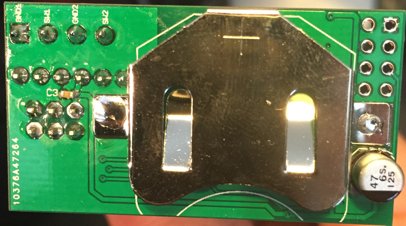
    Board Revision2 got delivered today and obviously i set about populating the board instantly!

    1_1455360799849_3.JPG 0_1455360799849_1.JPG

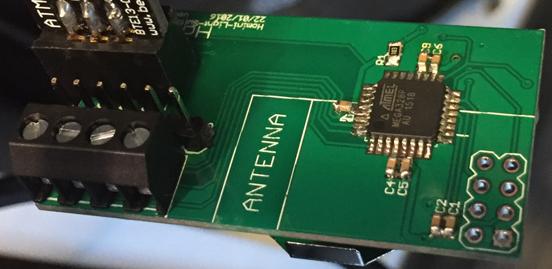
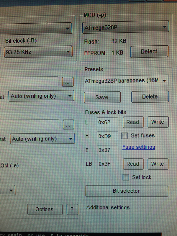
    I have the board all completed and now I'm attempting to burn the bootloader on. Before i go ahead and screw my IC up (I read if you use the wrong fuse reading for the timing of the clock you can't Re-burn anything else to it) i would like some advice. I've detected the current/pre-set fuse readings through AVRDUDESS using a clock speed of 93.75KHz, so i know the connection between my computer and the board is working. The readings for the fuses are below:
    0_1455360751069_2.JPG

    I'm currently using the fuse calculator here to workout the fuses needed. I'm also looking at Maniac's blog post here as he made a very low power module. The only thing i would question about his version/board is that his brownout is set to 2.7v. I've checked the nRF module and the lowest voltage it can go is 1.9, so maybe i should bring the BoD reading down even more or even disable it all together (I plan on reading the battery voltage from this module anyway).

    The below settings for the fuses are my own workings out with the fuse calculator linked above, I'm doubting myself here, i'm in territory that i'm not comfortable with so I'm more than likely making a mistake here but what do you think? The BoD is set to 1.8 here:

    Low: 0x62 | High: 0xD9 | Extended: 0xFE

    Once i have confirmed a fuse setting, Do I edit them into the board.txt config of Maniac's blog post or do I use that of @tekka's?


  • Hardware Contributor

    I have a very brief guide here, under 'Software'. There are some links to other guides as well. I think you use (42, DE, 07/FF) together with that linked bootloader (important).

    I also think Maniacs guide is a little old. You should get a a lot lower power by using MySensors lib and other some other tricks and settings.


  • Hardware Contributor

    @m26872 From having a quick look at your guide, you bring your clock speed right down to 1MHz, am i correct in thinking this? Do you have any timing issues at all, is the node still quick enough to respond to switching and sensor detecting or is there a delay in the signal sending?


  • Hardware Contributor

    @samuel235 Yes, it's working. But you can't use some things like DS18B20s and DHTs at these low frequencies. Si7021 etc are used instead. Button switches and other simple things are exellent applications.


  • Hardware Contributor

    @m26872 - Well, I was planning on maybe having a temp sensor in there at some point, but not this revision. So if i went without that function at the moment it wouldn't be the end of the world, i would just revise even more for the next revision. I'm presuming that you have taken it to 1MHz for power saving or?

    This is the configuration i'm thinking:

    ######## settings for 8Mhz internal clock

    proMYSBL8.name=ATmega328 internal 8Mhz with MYSBootloader
    proMYSBL8.upload.tool=avrdude
    proMYSBL8.upload.protocol=arduino
    proMYSBL8.upload.maximum_size=30720
    proMYSBL8.upload.maximum_data_size=2048
    proMYSBL8.upload.speed=57600
    proMYSBL8.bootloader.tool=avrdude
    proMYSBL8.bootloader.low_fuses=0x42
    proMYSBL8.bootloader.high_fuses=0xDE
    proMYSBL8.bootloader.extended_fuses=0xFF
    proMYSBL8.bootloader.unlock_bits=0x3F
    proMYSBL8.bootloader.lock_bits=0x3F
    proMYSBL8.bootloader.file=MySensors/MYSBootloader.hex
    proMYSBL8.build.mcu=atmega328p
    proMYSBL8.build.f_cpu=8000000L
    proMYSBL8.build.board=AVR_UNO
    proMYSBL8.build.core=arduino
    proMYSBL8.build.variant=standard

    That would remove the brownout, enable SPI, and put the clock to 8MHz. What is your thoughts on this config?


  • Hardware Contributor

    @samuel235

    • You'll need low MHz for ot to work when battery runs out and voltage decreases.
    • Those fuses are for 1MHz, not for 8MHz.
    • I've never used MYSBootloader. Someone else has to confirm the settings if you use this.

  • Hardware Contributor

    @m26872

    Lower clock speed would last through the low power phase of the battery. Obviously, thank you for pointing that out! However, I'm looking at Maniacs battery testing graph and the battery is stable down to around 2.4v for around 150 hours, then it will rapidly drop off to 0v, so I'm thinking "is the lower clock speed really worth the extra 10 hours of use?".

    The fuses, although I am going off of what you suggested, i entered them into my fuse calculator and its showing up at 8MHz, with no modification needed to the speed.... I'm a little confused at this part as you have now said that those fuses are for 1MHz.

    I'm now wondering if its worth using MYSBootloader or the one you used, I can see that you used this and programmed through the Arduino IDE, from your post you said you're more comfortable with using the Arduino IDE (Which i am too, but can adapt if needed).


  • Hardware Contributor

    @samuel235: don't worry about 1mhz...there is no big difference 1Mhz vs 8Mhz at 3V in deepsleep mode. In deepsleep mode, at 3V 8Mhz internal rc, you can get 140nA. So you can't have such interesting diff.
    In other hand, if node is wake up, you are in mA range, and here it can be interesting to play between clock and voltage 😉 you can do it on the fly in sketch and it's good to know that for timing things, atmel clock and voltage are linked.
    So i would suggest you to stay with internal rc 8Mhz, BOD 1.8V and MYSBootloader. If I remember right it should be ok. Other thing good to know, you can disable BOD=0V when in deepsleepmode (this is done like this in lib I think), but it's not a good practice to disable it when wake up. Keep 1.8V limit, it can prevent some bugs..All is described in datasheet 😉

    Another thing good to know, as I see lot of peope estimation for coincell...there are lot of chance that you can't get the full coincell capacity, depending on the application, the use. A common "prevision is to plan 80% of its capacity. It's due to the rate of discharge of battery and coincell's one is small..
    There are lot of others resources on the subjects but here few links :
    https://www.dmcinfo.com/Portals/0/Blog Files/High pulse drain impact on CR2032 coin cell battery capacity.pdf
    http://www.embedded.com/electronics-blogs/break-points/4429960/How-much-energy-can-you-really-get-from-a-coin-cell-
    http://www.ti.com/lit/wp/swra349/swra349.pdf


  • Hardware Contributor

    @scalz This is the information that was much needed. Right, so my settings are going to be:

    ######## settings for 8Mhz internal clock

    proMYSBL8.name=ATmega328 internal 8Mhz with MYSBootloader
    proMYSBL8.upload.tool=avrdude
    proMYSBL8.upload.protocol=arduino
    proMYSBL8.upload.maximum_size=30720
    proMYSBL8.upload.maximum_data_size=2048
    proMYSBL8.upload.speed=57600
    proMYSBL8.bootloader.tool=avrdude
    proMYSBL8.bootloader.low_fuses=0x62
    proMYSBL8.bootloader.high_fuses=0xD9
    proMYSBL8.bootloader.extended_fuses=0xFE
    proMYSBL8.bootloader.unlock_bits=0x3F
    proMYSBL8.bootloader.lock_bits=0x3F
    proMYSBL8.bootloader.file=MySensors/MYSBootloader.hex
    proMYSBL8.build.mcu=atmega328p
    proMYSBL8.build.f_cpu=8000000L
    proMYSBL8.build.board=AVR_UNO
    proMYSBL8.build.core=arduino
    proMYSBL8.build.variant=standard

    At the moment the fuses are set using Hexadecimal notation, I'm sure that I read somewhere that to burn this using a Arduino IDE you need to use normal binary rather than Hex. Do you know if Hex is okay for Arduino IDE?

    I've got those fuses set to enable 1.8v BoD, 8MHz clock with a 65ms delay on startup. This will use MYSBootloader too. Does this sound okay to now edit my boards.txt, and burn the MYSBootloader.hex file to the chip? I'm using a USBASP device connected to my ISP connection. Am i forgetting anything at all here? As far as I'm aware of, i now plug the board and USBASP into my computer, load the .hex file into arduino IDE and burn using the board config i have put into my boards.txt file. Then i can use my FTDI adapter to then burn sketches to the board through the arduino IDE?

    I know that to some people I may be asking what seems like the same questions over and over but I'm starting to feel very confident with embedded chips now. Thank you!


  • Hardware Contributor

    no problem 🙂 yes, it sounds ok...that's how I do too. But I don't use mysbootloader, i use dualoptiboot (sensebender bootloader). for the hex/bin fuse notation, I use hexa.


  • Hardware Contributor

    @samuel235

    • You could be rigth regarding the battery. I've no coin cell experience.
    • You noticed the check mark by the 'divide clock by 8' ?
    • If you by 'program' normal ftdi flash, then yes. I didn't program bootloader with Arduino.

  • Hardware Contributor

    @scalz

    Is there a reason to use dualoptiboot over MYSBootloader or is that just something you did for no reason?

    Did you use Arduino IDE to burn your bootloader, if so then i can confirm its okay to use Hexa for my board with arduino IDE, if you didn't i will have to convert it to normal binary.

    @m26872

    I have just realised that you burn your bootloader with the check mark of 8MHz but then the board.txt is configured to set it to 1MHz, is that what you're trying to tell me? I'm not too sure on your last point, i don't get what you're trying to say if i'm honest, could you elaborate a little? Sorry.


  • Hardware Contributor

    @samuel235: yes, always good reasons 😉 I have tried both. both works well. I like the "buffer style" of dualoptiboot. plus no mysensors lib in bootloader, few others reasons...but mysbootloader is very cool too and simple. So don't worry about this 🙂 it's a matter of taste, each have their pros&cons.
    Yes, use arduino ide to burn bootloader + hexa is ok.


  • Hardware Contributor

    @scalz - Perfect. I will see how i get on with the MYSBootloader style. Soon as i get back i will burn these settings to my uC and see how i get on. I will come back with the results when i'm done. 🙂


  • Hardware Contributor

    @scalz

    • Don't know if good practice or not, but I run 328p + nRF down to 1.6V very stable. Could depend on a lot things and conditions of course. You said "some bugs" - do you know more what risks there are? Permanent damages etc?
    • Do you know if the 'Divide clock by 8" (8MHz or 1MHz) also can be changed on-fly-with code? If so, does it matter which speed set by fuse and thus used at start-up?
    • Great thanks for the coin cell info!

  • Hardware Contributor

    @samuel235 I meant that you should untick this to use 8MHz. Provided that you don't change it on-the-fly somehow.
    0_1455459198626_klipp.PNG


  • Hardware Contributor

    @samuel235 Sorry for not elaborating. I've been mobile all day until now. And my phone also seems to have a few issues with the forum.


  • Hardware Contributor

    @m26872 Ahh right okay, good job i caught your reply before burning it haha! So if i set it to 8MHz internal with 64ms delay and untick that divide by 8 option, that'll be good?


  • Hardware Contributor

    Yes. but don't forget to enable the boot reset vector.


  • Hardware Contributor

    @samuel235 I have not checked if the bootloader size and baud rate matches fuse settings.


  • Hardware Contributor

    @m26872:

    • for bod=0v, problems could be flash corruption for instance..so it's good to know (it's explained in datasheet that for instance it ensures that a flash write is completely done before reset, I think it makes sense, plus I imagine that there are some internal things with voltage levels related stuff. but I'm not a guru on this....). So my interpretation is sometimes we don't care about it for sleepmode, for instance, and sometimes in wakeup, it's important or not, depending of tasks involved...
      maybe I should have said a good practice is to know what you do, lol!
    • for prescaler, are you asking for something like this : http://www.gammon.com.au/forum/?id=11497&reply=7#reply7
    • glad to share what I learn 🙂

  • Hardware Contributor

    @scalz .

    maybe I should have said a good practice is to know what you do, lol!

    l don't fulfil that either, lol! 😃

    Thanks for the prescaler info. Seems like a yes - it can be changed on-the-fly, but for me it's a No. I won't even dare to think of consequences for the rest of the software.


  • Hardware Contributor

    @m26872 said:

    @samuel235 I have not checked if the bootloader size and baud rate matches fuse settings.

    I'm not 100% sure of what you mean here, on the fuse calculator there is not an option to specify the baud rate.... As for the bootloader size, the calculator is set to "Boot Flash section size=2048 words Boot start address=$3800; [BOOTSZ=00]". As this is the highest it can be I'm assuming it is correct, however i will try and check the size of the MYSBootloader.hex size and see if it is below 2048 words (Is this what this setting means?).


  • Hardware Contributor

    @samuel235 No, but bootloader and boards.txt must have same buad rate. I think you already have the correct though since 8MHz is pretty much standard clock speed. Slower clock would require lower buad rate.


  • Hardware Contributor

    @m26872 Is there a way to read the .hex file to see the specified baud rate before i go and brick the chip? Also, just to confirm, i have to burn the fuse settings in AVRDUDE then burn the bootloader with arduino IDE. Is there anything I'm failing to understand, i only have one more uC here at the moment and i don't want to brick several of them 😞


  • Hardware Contributor

    @samuel235 Sorry, I can't help you further. I don't know for sure about these things.


  • Hardware Contributor

    @m26872 - That is okay, I think I'm pretty safe to assume that it is correct as it is what is provided on Tekka's guide. So I'm going to attempt to burn the fuses at E2 D8 FE. Once I've done that (and it works fine), Arduino IDE should burn the bootloader onto the uC without an issue and then i can just upload a arduino sketch, right? o.O


  • Hardware Contributor

    I've just written the fuse settings and got this log report:

    avrdude.exe: set SCK frequency to 187500 Hz
    avrdude.exe: AVR device initialized and ready to accept instructions
    
    Reading | ################################################## | 100% -0.00s
    
    avrdude.exe: Device signature = 0x1e950f
    avrdude.exe: reading input file "0xE2"
    avrdude.exe: writing lfuse (1 bytes):
    
    Writing | ################################################## | 100% -0.00s
    
    avrdude.exe: 1 bytes of lfuse written
    avrdude.exe: verifying lfuse memory against 0xE2:
    avrdude.exe: load data lfuse data from input file 0xE2:
    avrdude.exe: input file 0xE2 contains 1 bytes
    avrdude.exe: reading on-chip lfuse data:
    
    Reading | ################################################## | 100% -0.00s
    
    avrdude.exe: verifying ...
    avrdude.exe: 1 bytes of lfuse verified
    avrdude.exe: reading input file "0xD8"
    avrdude.exe: writing hfuse (1 bytes):
    
    Writing | ################################################## | 100% 0.02s
    
    avrdude.exe: 1 bytes of hfuse written
    avrdude.exe: verifying hfuse memory against 0xD8:
    avrdude.exe: load data hfuse data from input file 0xD8:
    avrdude.exe: input file 0xD8 contains 1 bytes
    avrdude.exe: reading on-chip hfuse data:
    
    Reading | ################################################## | 100% 0.00s
    
    avrdude.exe: verifying ...
    avrdude.exe: 1 bytes of hfuse verified
    avrdude.exe: reading input file "0xFE"
    avrdude.exe: writing efuse (1 bytes):
    
    Writing |  ***failed;  
    ################################################## | 100% 0.09s
    
    avrdude.exe: 1 bytes of efuse written
    avrdude.exe: verifying efuse memory against 0xFE:
    avrdude.exe: load data efuse data from input file 0xFE:
    avrdude.exe: input file 0xFE contains 1 bytes
    avrdude.exe: reading on-chip efuse data:
    
    Reading | ################################################## | 100% 0.00s
    
    avrdude.exe: verifying ...
    avrdude.exe: verification error, first mismatch at byte 0x0000
                 0x06 != 0xfe
    avrdude.exe: verification error; content mismatch
    
    avrdude.exe done.  Thank you.
    

    I then checked the fuses by reading them. I can confirm it has written the Low and the High fuse but as the log says, it failed to write the extended. So I went to the calculator site and read the following (This is what i was asking about hex vs binary for):

    "Note that some numerical values refer to fuses containing undefined bits (set to '1' here). Depending on the target device these fuse bits will be read either as '0' or '1'. Verification errors will occur if the values are read back with undefined bits set to '0'. Everything is fine if the values read from the device are either the same as programmed, or the following values (undefined set to '0'): Extended: 0x06."

    I then attempted to burn the bootloader, assuming the error is fine to skip (as the fuse calculator said), but it gave me the same error of:

    avrdude: verification error, first mismatch at byte 0x0000
             0x06 != 0xfe
    avrdude: verification error; content mismatch
    

    So basically, telling me that my boards.txt is telling the IDE that the fuse should be FE, but its 06.


  • Hardware Contributor

    Looks like ext fuse is already 0x06 and you only need to change your board.txt to the same. I've never heard before that the 0xFE type of writing should work in avrdude/Arduino IDE.


  • Hardware Contributor

    I went ahead and changed my board.txt to reflect 0x06, to check. It passed through and burnt the bootloader. However, if i try to upload a sketch (using the FTDI adapter that i have, this) I get a timing error. How do i upload a sketch to the chip with the ISP connection (just to test if my FTDI pins are wired incorrectly). This is my log from arduino IDE:

    Sketch uses 12,610 bytes (41%) of program storage space. Maximum is 30,720 bytes.
    Global variables use 398 bytes (19%) of dynamic memory, leaving 1,650 bytes for local variables. Maximum is 2,048 bytes.
    avrdude: stk500_recv(): programmer is not responding
    avrdude: stk500_getsync() attempt 1 of 10: not in sync: resp=0x7c
    avrdude: stk500_recv(): programmer is not responding
    avrdude: stk500_getsync() attempt 2 of 10: not in sync: resp=0x7c
    avrdude: stk500_recv(): programmer is not responding
    avrdude: stk500_getsync() attempt 3 of 10: not in sync: resp=0x7c
    avrdude: stk500_recv(): programmer is not responding
    avrdude: stk500_getsync() attempt 4 of 10: not in sync: resp=0x7c
    avrdude: stk500_recv(): programmer is not responding
    avrdude: stk500_getsync() attempt 5 of 10: not in sync: resp=0x7c
    avrdude: stk500_recv(): programmer is not responding
    avrdude: stk500_getsync() attempt 6 of 10: not in sync: resp=0x7c
    avrdude: stk500_recv(): programmer is not responding
    avrdude: stk500_getsync() attempt 7 of 10: not in sync: resp=0x7c
    avrdude: stk500_recv(): programmer is not responding
    avrdude: stk500_getsync() attempt 8 of 10: not in sync: resp=0x7c
    avrdude: stk500_recv(): programmer is not responding
    avrdude: stk500_getsync() attempt 9 of 10: not in sync: resp=0x7c
    avrdude: stk500_recv(): programmer is not responding
    avrdude: stk500_getsync() attempt 10 of 10: not in sync: resp=0x7c
    Problem uploading to board.  See http://www.arduino.cc/en/Guide/Troubleshooting#upload for suggestions.
    

    "programmer is not responding" - I was asking myself "Would this mean that arduino IDE can't use avrdude for some reason?" but then i figured that it used it to burn the bootloader so that isnt right. Is it trying to find the ISP programmer and cant because i'm connected through FTDI maybe?


  • Hardware Contributor

    I have just remembered that if you go to the file menu in Arduino IDE you get the option to upload using programmer. I have just done this through my SPI programmer, it has uploaded correctly. I will now solder the nRF module onto the board and i will report back with my results. Crosses fingers


  • Hardware Contributor

    BINGO!!

    We have a working coin cell powered light switch.
    2_1455483349684_image.jpeg 1_1455483349683_image.jpeg 0_1455483349682_image.jpeg

    I will upload some decent images later on tonight or tomorrow.

    I'de just like to talk everyone that has contributed to this thread/post and enabled me to create my first of many embedded projects. I'm applying for a University course in september for Computer Science (Smart Technologies), all about embedded systems, drones, home automation etc etc. This is just the beginning!

    I'll get this project up on OpenHardware.io asap as Version 1 and we can build on this as a base plate for futher projects.


  • Hardware Contributor

    Now, the next two steps I'm interested in taking is to get this working with 2 switches (Software modification, should be simple) and then to have it report its remaining power every 30 minutes to allow me to set up notifications through openhab to alert me to change the batteries so I'm not left with no light switch.


  • Hardware Contributor

    It would appear that I'm having a timing issue with uploading via the FTDI adapter. Would this be down to the speed of the uC effecting the RX and TX connections?


  • Hardware Contributor

    This post is deleted!

  • Hardware Contributor

    @samuel235 Are you trying to upload with Ftdi serial to MYSbootloader? I think it's only for OTA uploads, if you read here.


  • Hardware Contributor

    @m26872 - Thank you for pointing this out to me. I'm unsure why I haven't stumbled across that thread/topic today of all days, been searching and reading about MYSBootloader all day >.<

    From personal experience, would you advise any other bootloader, I'm guessing you're going to tell me about the one you are using. Could you link any information for me to check out regarding your choice of bootloader?

    Am I correct in recalling you're using DualOptiBoot?
    Does DualOptiBoot need external memory/flash?


  • Hardware Contributor

    @samuel235 No, I use plain optiboot, but I couldn't find a suiteable precompiled one for you. DualOptiboot requires external flash as you say.
    It's been a while since I played with bootloaders, but I think normal 8MHz Arduino Pro Mini bootloader would work for you with internal clock as well. It's this [ATmegaBOOT_168_atmega328_pro_8MHz.hex ] and I can find it in my "C:\Program Files\Arduino\hardware\arduino\avr\bootloaders\atmega" -folder, should be about the same for you I think. Try fuse settings E2-DA-06 (Lo-Hi-Ex) and rest of the boards.txt-settings from ArduinoProMini 3.3V 8MHz.


  • Hardware Contributor

    @m26872 - Ahh the generic arduino bootloader... I will have a look into using that tomorrow. As the MYSController gets more feature rich and support i will use that setup, however i love OpenHAB way too much to switch over right now.


  • Hardware Contributor

    @m26872 - I've just spent a few minutes looking through my boards.txt and i came across:

    ######## Settings for 
    
    ATmega328 8MHz Internal clock
    atmega328bb.name=ATmega328 on a breadboard (8MHz internal clock)
    atmega328bb.upload.protocol=stk500
    atmega328bb.upload.maximum_size=30720
    atmega328bb.upload.speed=57600
    atmega328bb.bootloader.low_fuses=0xE2
    atmega328bb.bootloader.high_fuses=0xDA
    atmega328bb.bootloader.extended_fuses=0x05
    atmega328bb.bootloader.path=arduino:atmega
    atmega328bb.bootloader.file=ATmegaBOOT_168_atmega328_pro_8MHz.hex
    atmega328bb.bootloader.unlock_bits=0x3F
    atmega328bb.bootloader.lock_bits=0x0F
    atmega328bb.build.mcu=atmega328p
    atmega328bb.build.f_cpu=8000000L
    atmega328bb.build.core=arduino:arduino
    atmega328bb.build.variant=arduino:standard
    

    Then out of interest I thought I would look at the bootloader that you suggested, to see what difference there would be. Turns out I was actually looking at it without knowing. I have a feeling that if I change the fuse settings to those that i am using now with MYSBootloader, I will be set to go.

    The High Fuse setting you provided enables 1024 words in the boot flash section, a couple of questions about this:

    • Is this defining the size of the area needed for the bootloader section on the built in memory (So smaller this is set to, as long as the bootloader will fit, the more room I will have for a sketch)?
    • How do i find out the 'word size' of the bootloader (if the first question is correct method) so I can determine if the 1024 is big enough? I would rather know how to work this out rather than just assuming that it is because it is specified as that as default.

    I was going to leave my fuses where they were at (E2, D8, 06 as LO:HI:EX) but if I can change the boot size setting, that would allow a bigger room for my sketches = Win Win!

    I'm still slightly confused as to not being able to burn my extended fuse. I have read somewhere (lost the page) about not being possible to burn an EX fuse on a ATmega328p, which i find very hard to believe.


  • Hardware Contributor

    @samuel235 said:

    • Is this defining the size of the area needed for the bootloader section on the built in memory (So smaller this is set to, as long as the bootloader will fit, the more room I will have for a sketch)?

    Yes.

    • How do i find out the 'word size' of the bootloader (if the first question is correct method) so I can determine if the 1024 is big enough? I would rather know how to work this out rather than just assuming that it is because it is specified as that as default.

    I don't have the tool or knowledge for that. Should be doable by removing indices and count the bytes in hex-file. But for me it's not a big deal to just use the size settings recommended for a particular bootloader. And in this case it´s stock Arduino, so why question it.

    I'm still slightly confused as to not being able to burn my extended fuse. I have read somewhere (lost the page) about not being possible to burn an EX fuse on a ATmega328p, which i find very hard to believe.

    So the '0x06'-kind of notation didn't work either? Strange.


  • Hardware Contributor

    @m26872 said:

    And in this case it´s stock Arduino, so why question it.

    I'm not questioning it, I just wanted to learn how to do it for if i ever came across a need to modify a bootloader i would then know how to record its size for the fuse burning.

    So the '0x06'-kind of notation didn't work either? Strange.

    When i set the boards.txt file to read 0x06 it worked perfect, which insinuates that it couldn't burn the chosen BoD, even though the fuse calculator says to ignore the error of the extended fuse, it should burn it even though it gives the error. I'm interested in trying to burn the extended fuse in normal binary rather than hexa. But i doubt it would work anyway.


  • Hardware Contributor

    It has just clicked inside my busy mind that 0x06 in binary is the same as 0xFE in Hexa. How embarrassed am I now after many questions and hours thinking about the extended fuse value. I'm now assuming that it returns the error because it is already set at that fuse 😳


  • Hardware Contributor

    So, i have it working using the following board.txt config:

    ######## Settings for 
    
    ATmega328 8MHz Internal clock Brown-out detection 1.8v
    atmega328bb.name=ATmega328 on a breadboard (8MHz internal clock) BoD1.8
    atmega328bb.upload.tool=avrdude
    atmega328bb.upload.protocol=stk500
    atmega328bb.upload.maximum_size=30720
    atmega328bb.upload.speed=57600
    atmega328bb.bootloader.tool=avrdude
    atmega328bb.bootloader.low_fuses=0xE2
    atmega328bb.bootloader.high_fuses=0xDA
    atmega328bb.bootloader.extended_fuses=0x06
    atmega328bb.bootloader.path=arduino:atmega
    atmega328bb.bootloader.file=atmega/ATmegaBOOT_168_atmega328_pro_8MHz.hex
    atmega328bb.bootloader.unlock_bits=0x3F
    atmega328bb.bootloader.lock_bits=0x3F
    atmega328bb.build.mcu=atmega328p
    atmega328bb.build.f_cpu=8000000L
    atmega328bb.build.core=arduino:arduino
    atmega328bb.build.variant=arduino:standard
    

    However, no matter what I did I couldn't get it to upload via FTDI. I've tried looking at the Arduino Pro Mini settings in boards.txt to see what 'upload.tool' it uses, AVRDUDE, same as i specified. I also then went to the google docs for the boards.txt reference file, that advises everything i did too. I'm a little stumped. All that i can think of is that i have wired it incorrectly on the pcb. Whats your thoughts on this?


  • Hardware Contributor

    @samuel235 said:

    I'm not questioning it,

    I'm not saying you do, I just told how I think of it.

    I'm interested in trying to burn the extended fuse in normal binary rather than hexa.

    Why, when the result is exactly the same?
    Also, I'm not familiar with from where the "binary or hexa" comes from? They're both hexadecimal notation as far as I can see.


  • Hardware Contributor

    I'm not sure what is your problem with ftdi.maybe wirings...do you have cts to gnd, and of course dtr to dtr, only one vcc active...??? Maybe you should try to burn original arduino ide bootloader and then ftdi upload attempts. If it still doesn't work, it could be the wirings...
    for hexa vs binary..in some case binary notation can be useful, but for fuses, I prefer hexa: shorter, no possibility of mistakes by missing/miscounting one "1" or "0" bit 😉


  • Hardware Contributor

    @m26872 - I wanted to try it because i'm sure i read somewhere that the ATmega328 can't accept Hexa as fuses. But i doubt that information is valid if i'm honest with you.

    @scalz - I have dtr to dtr and cts linked to ground. I also only have one VCC pin (which obviously goes to VCC). I'll be perfectly honest with you; the boart.txt setting i posted above, i thought that was using the arduino .hex bootloader, please inform me if i'm in correct in that.


  • Hardware Contributor

    This is the board layout, if you guys can see any issues with my FTDI connections/pinout please advice me that you do, I will get that sorted for revison 3 of the board. If i'm honest, I don't mind burning the sketches with the ISP programmer everytime, so I'm very tempted to remove the FTDI, allowing a smaller board still.
    0_1455731784013_Wiring.jpg


  • Hardware Contributor

    @samuel235 How do you debug through ISP ?
    Have you tested your FTDI USB-serial converter with ArduinoProMini or something?


  • Hardware Contributor

    @m26872 - I haven't tried it out with a arduino pro mini, because i don't have one. However, tomorrow, I will get a Arduino nano out and sort some testing of my FTDI converter on that. I'm hoping that works and its just a simple wiring issue on my board.

    From your statement of "How do you debug through ISP?" I'm guessing that it isn't possible too, or was that a genuine question? If its not possible then I will keep the FTDI connectors on the board.


Suggested Topics

20
Online

11.2k
Users

11.1k
Topics

112.5k
Posts