CNC PCB milling
-
@andrew Great that you're back. Did you alter your max speed and max acceleration values at all from the defaults? You didn't list them in your earlier list of magic numbers.
@neverdie I still use my default settings (see below). I re-applied these settings after I flashed the board to grbl 1.1f.
to be honest, after I found the right parameters for the PCB milling jobs I did not went further to fine tune the CNC settings, due to the lack of time. maybe later of the year, but currently I'm more than happy with the results.$0=10 (step pulse, usec) $1=25 (step idle delay, msec) $2=0 (step port invert mask:00000000) $3=5 (dir port invert mask:00000101) $4=0 (step enable invert, bool) $5=0 (limit pins invert, bool) $6=0 (probe pin invert, bool) $10=3 (status report mask:00000011) $11=0.010 (junction deviation, mm) $12=0.002 (arc tolerance, mm) $13=0 (report inches, bool) $20=0 (soft limits, bool) $21=0 (hard limits, bool) $22=0 (homing cycle, bool) $23=0 (homing dir invert mask:00000000) $24=25.000 (homing feed, mm/min) $25=500.000 (homing seek, mm/min) $26=250 (homing debounce, msec) $27=1.000 (homing pull-off, mm) $100=800.000 (x, step/mm) $101=800.000 (y, step/mm) $102=800.000 (z, step/mm) $110=800.000 (x max rate, mm/min) $111=800.000 (y max rate, mm/min) $112=500.000 (z max rate, mm/min) $120=10.000 (x accel, mm/sec^2) $121=10.000 (y accel, mm/sec^2) $122=10.000 (z accel, mm/sec^2) $130=200.000 (x max travel, mm) $131=200.000 (y max travel, mm) $132=200.000 (z max travel, mm)``` -
@neverdie I still use my default settings (see below). I re-applied these settings after I flashed the board to grbl 1.1f.
to be honest, after I found the right parameters for the PCB milling jobs I did not went further to fine tune the CNC settings, due to the lack of time. maybe later of the year, but currently I'm more than happy with the results.$0=10 (step pulse, usec) $1=25 (step idle delay, msec) $2=0 (step port invert mask:00000000) $3=5 (dir port invert mask:00000101) $4=0 (step enable invert, bool) $5=0 (limit pins invert, bool) $6=0 (probe pin invert, bool) $10=3 (status report mask:00000011) $11=0.010 (junction deviation, mm) $12=0.002 (arc tolerance, mm) $13=0 (report inches, bool) $20=0 (soft limits, bool) $21=0 (hard limits, bool) $22=0 (homing cycle, bool) $23=0 (homing dir invert mask:00000000) $24=25.000 (homing feed, mm/min) $25=500.000 (homing seek, mm/min) $26=250 (homing debounce, msec) $27=1.000 (homing pull-off, mm) $100=800.000 (x, step/mm) $101=800.000 (y, step/mm) $102=800.000 (z, step/mm) $110=800.000 (x max rate, mm/min) $111=800.000 (y max rate, mm/min) $112=500.000 (z max rate, mm/min) $120=10.000 (x accel, mm/sec^2) $121=10.000 (y accel, mm/sec^2) $122=10.000 (z accel, mm/sec^2) $130=200.000 (x max travel, mm) $131=200.000 (y max travel, mm) $132=200.000 (z max travel, mm)```@andrew said in CNC PCB milling:
@neverdie I still use my default settings (see below). I re-applied these settings after I flashed the board to grbl 1.1f.
to be honest, after I found the right parameters for the PCB milling jobs I did not went further to fine tune the CNC settings, due to the lack of time. maybe later of the year, but currently I'm more than happy with the results.$0=10 (step pulse, usec) $1=25 (step idle delay, msec) $2=0 (step port invert mask:00000000) $3=5 (dir port invert mask:00000101) $4=0 (step enable invert, bool) $5=0 (limit pins invert, bool) $6=0 (probe pin invert, bool) $10=3 (status report mask:00000011) $11=0.010 (junction deviation, mm) $12=0.002 (arc tolerance, mm) $13=0 (report inches, bool) $20=0 (soft limits, bool) $21=0 (hard limits, bool) $22=0 (homing cycle, bool) $23=0 (homing dir invert mask:00000000) $24=25.000 (homing feed, mm/min) $25=500.000 (homing seek, mm/min) $26=250 (homing debounce, msec) $27=1.000 (homing pull-off, mm) $100=800.000 (x, step/mm) $101=800.000 (y, step/mm) $102=800.000 (z, step/mm) $110=800.000 (x max rate, mm/min) $111=800.000 (y max rate, mm/min) $112=500.000 (z max rate, mm/min) $120=10.000 (x accel, mm/sec^2) $121=10.000 (y accel, mm/sec^2) $122=10.000 (z accel, mm/sec^2) $130=200.000 (x max travel, mm) $131=200.000 (y max travel, mm) $132=200.000 (z max travel, mm)```Looks like the only difference is that your default max rates for x and y were 800, whereas mine were 5000, and your max rate for z was 500, whereas my default was 800 before I cut it by 50% to 400.
In the interest of minimizing differences, I'll adopt your defaults instead.
-
@neverdie said in CNC PCB milling:
@andrew Are you planning to provide more detail about how to setup and do double sided PCBs, or is it pretty much RTFM at this point? Just wondering. Your earlier posts were very thorough and helped a lot.
did you manage to create double sided PCB jobs in the meantime based on my suggestion and on flatcam's documentation? it is not a hardcore process, let me know if you stuck at a given step.
regarding to the mentioned upgrades. I agree with @executivul, it doesn't worth to do that with this machine. feedback from steppers, elevation measuring etc are overkill.
it's capabilities are more than enough for very precise pcb milling, if you would like to do much more with it, then a different machine could be better instead. if you have issues with the results, then it is configuration / settings / cnc job issue. if you loose steps, then the given stepper driver is not properly adjusted (did you checked the pololu driver configuration from the linked documentation?) or your tool/spindle speed/cutting depth/feed rate is not good for the given job.
@andrew said in CNC PCB milling:
did you manage to create double sided PCB jobs in the meantime based on my suggestion and on flatcam's documentation? it is not a hardcore process, let me know if you stuck at a given step.
Not sure what kind of pins to use for the alignment.
-
Even after all this tweaking, the z-axis was off by 0.048mm after the latest set of probing.
-
Even after all this tweaking, the z-axis was off by 0.048mm after the latest set of probing.
@neverdie said in CNC PCB milling:
Even after all this tweaking, the z-axis was off by 0.048mm after the latest set of probing.
What do you mean by "off"? Afaik grbl doesn't have a M48 equivalent command for probe/machine repeatability... So it can't probe the same place automatically. You have to write your own code for that, based on G32.2 command, take a few measurements and see the difference.
If you mean across the whole board, depending on the size of the measured area that's not bad at all. -
Even after all this tweaking, the z-axis was off by 0.048mm after the latest set of probing.
-
@neverdie could you please explain how did you find/measure this? also please let me know the details of the executed job, including the G code generation properties/settings (e.g. feed rate, depth, multiple passes etc.) used in flatcam.
@andrew said in CNC PCB milling:
could you please explain how did you find/measure this?
- Decided upon an origen. Used Chilipeppr to "run test probe" to find the zero z-height. Zeroed x,y,z at that location.
- Did an autolevel, at 1mm spacing, over a 20x10mm area.
- Following this, returned to x=0, y=0. Ran another test probe. Ideally it would have come back as z=0. Instead, it came back as z=-0.048.
So, if at that point I were to actually run g-code with a cutting depth of z=-0.05, it would barely scratch the surface. Somehow during the 1mm autolevel probing, z became uncalibrated. If I were to re-zero z based on the second test probe, it would cut, but the cutting depth wouldn't be uniform.
Anyhow, my new rule is that if I come across a situation like the above, I throw out the auto-leveling and start over rather than executing the g-code. Often, the next autoleveling will have less discrepancy by step 3.
-
@neverdie
Maybe run step 1
Then run some g-code but above the job.(for a few mins).
Then run step 3.
This could be an autolevel problem.@rmtucker said in CNC PCB milling:
Maybe run step 1
Then run some g-code but above the job.(for a few mins).
Then run step 3.How might that help?
-
@rmtucker said in CNC PCB milling:
Maybe run step 1
Then run some g-code but above the job.(for a few mins).
Then run step 3.How might that help?
-
@neverdie
What if you have broken .048 off the end of the tool during autolevel?
So run some g-code above the job then re-probe so you know you have not twatted the tool.:relaxed:@rmtucker said in CNC PCB milling:
What if you have broken .048 off the end of the tool during autolevel?
Good point. I'll have a closer look for that the next time it happens.
Also, I'll try repeating the test using a dull bit (which presumably won't break) and see whether it still happens or not.
Thanks!
-
@NeverDie grbl 1.1 probing command is G38.2 Z-10 F25 where Z tells it how low should go before erroring if it doesn't touch and F is the speed.
You should try manually issuig G38, then G92 Z0 to set new Z0 position and then finally G0 Z10 F100 to lift the probe, rinse and repeat without the G92, how repeatable is the reading, does it stay at 10.00?
Then do the air job, or some simple moving (G0 X5 Y5 Z5, G0 X0 Y0 Z10 a few times )and retest manually with G38LE. The probing command is G38.2, I've edited the post to correct it.
-
@andrew said in CNC PCB milling:
could you please explain how did you find/measure this?
- Decided upon an origen. Used Chilipeppr to "run test probe" to find the zero z-height. Zeroed x,y,z at that location.
- Did an autolevel, at 1mm spacing, over a 20x10mm area.
- Following this, returned to x=0, y=0. Ran another test probe. Ideally it would have come back as z=0. Instead, it came back as z=-0.048.
So, if at that point I were to actually run g-code with a cutting depth of z=-0.05, it would barely scratch the surface. Somehow during the 1mm autolevel probing, z became uncalibrated. If I were to re-zero z based on the second test probe, it would cut, but the cutting depth wouldn't be uniform.
Anyhow, my new rule is that if I come across a situation like the above, I throw out the auto-leveling and start over rather than executing the g-code. Often, the next autoleveling will have less discrepancy by step 3.
@neverdie said in CNC PCB milling:
@andrew said in CNC PCB milling:
could you please explain how did you find/measure this?
- Decided upon an origen. Used Chilipeppr to "run test probe" to find the zero z-height. Zeroed x,y,z at that location.
- Did an autolevel, at 1mm spacing, over a 20x10mm area.
- Following this, returned to x=0, y=0. Ran another test probe. Ideally it would have come back as z=0. Instead, it came back as z=-0.048.
So, if at that point I were to actually run g-code with a cutting depth of z=-0.05, it would barely scratch the surface. Somehow during the 1mm autolevel probing, z became uncalibrated. If I were to re-zero z based on the second test probe, it would cut, but the cutting depth wouldn't be uniform.
Anyhow, my new rule is that if I come across a situation like the above, I throw out the auto-leveling and start over rather than executing the g-code. Often, the next autoleveling will have less discrepancy by step 3.
if your probe speed is too fast, then it could push the pcb at the given points and also it could damage your tip's end, as it was mentioned by @rmtucker, which could cause this issue as well.
-
@andrew said in CNC PCB milling:
did you manage to create double sided PCB jobs in the meantime based on my suggestion and on flatcam's documentation? it is not a hardcore process, let me know if you stuck at a given step.
Not sure what kind of pins to use for the alignment.
@neverdie said in CNC PCB milling:
@andrew said in CNC PCB milling:
did you manage to create double sided PCB jobs in the meantime based on my suggestion and on flatcam's documentation? it is not a hardcore process, let me know if you stuck at a given step.
Not sure what kind of pins to use for the alignment.
I missed this reply from you.
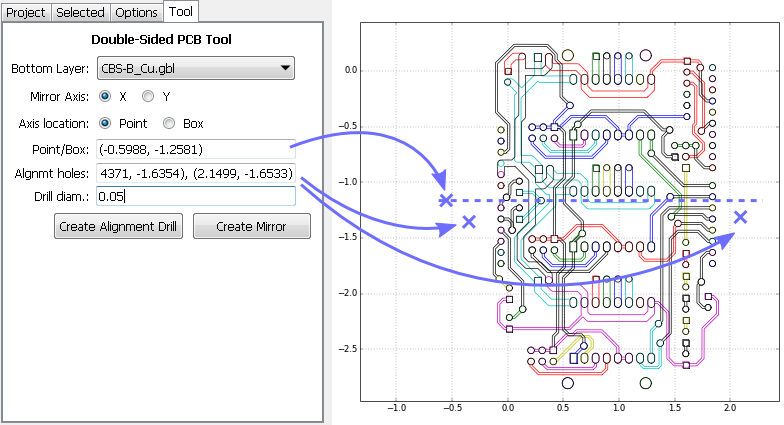
so, you have to define the alignment holes, typically outside of the actual pcb area, in the "frame".
you have to define two of them, the rest will be calculated automatically.the steps are exactly the same as that you can see on http://flatcam.org/manual/procedures.html#side-pcb
see the pic below. note, that you don't have to write the coordinates to the input boxes manually, once you click on the design area the corresponding coordinates will be copied to the clipboard, so you can use ctrl-v to fill out the settings.
- click on the picture to define the axis (X in this example)
- copy the corresponding coordinates to the point/box input filed
- click on the design area to define the exact location of the first alignment hole (left side of the actual pcb)
- copy the corresponding coordinates to the alignment holes input filed
- click on the design area to define the exact location of the first alignment hole (right side of the actual pcb)
- copy the corresponding coordinates to the alignment holes input filed. the two set of coordinates have to be separated by coma.
- configure the alignment holes' drill size
- click on the create align drill button and you're done. back on the project tab you can find a new drill job which you have to further process to create the belonging G code from it.
-
@neverdie said in CNC PCB milling:
@andrew said in CNC PCB milling:
did you manage to create double sided PCB jobs in the meantime based on my suggestion and on flatcam's documentation? it is not a hardcore process, let me know if you stuck at a given step.
Not sure what kind of pins to use for the alignment.
I missed this reply from you.
so, you have to define the alignment holes, typically outside of the actual pcb area, in the "frame".
you have to define two of them, the rest will be calculated automatically.the steps are exactly the same as that you can see on http://flatcam.org/manual/procedures.html#side-pcb
see the pic below. note, that you don't have to write the coordinates to the input boxes manually, once you click on the design area the corresponding coordinates will be copied to the clipboard, so you can use ctrl-v to fill out the settings.
- click on the picture to define the axis (X in this example)
- copy the corresponding coordinates to the point/box input filed
- click on the design area to define the exact location of the first alignment hole (left side of the actual pcb)
- copy the corresponding coordinates to the alignment holes input filed
- click on the design area to define the exact location of the first alignment hole (right side of the actual pcb)
- copy the corresponding coordinates to the alignment holes input filed. the two set of coordinates have to be separated by coma.
- configure the alignment holes' drill size
- click on the create align drill button and you're done. back on the project tab you can find a new drill job which you have to further process to create the belonging G code from it.
-
@andrew Are you using male header pins for your alignment? How deep are you drilling the holes them?
-
@neverdie yes, I use male pins, with 0.7mm drill (so it is tight for the pin), 5mm depth. but this is really up to you, choose anything which you have easy access to.
With single sided PCB, I soldered the ground wire (for probing) to the copper cladding, just as the Chilipeppr author did. How are you handling it for two sided? If I do it that way for two sided, the solder bump may prevent the board laying flat on the wasteboard.
-
With single sided PCB, I soldered the ground wire (for probing) to the copper cladding, just as the Chilipeppr author did. How are you handling it for two sided? If I do it that way for two sided, the solder bump may prevent the board laying flat on the wasteboard.
@neverdie I use a wood screw in the sacrificial board holding a piece of metal as a "clamp" I slide it over the board (1mm overlap) and clip one alligator clip to the screw, the other to the bit. After probing I slide it out of the way. The metal piece is about 10cm long and it's left in place for the life of the wood board.
-
With single sided PCB, I soldered the ground wire (for probing) to the copper cladding, just as the Chilipeppr author did. How are you handling it for two sided? If I do it that way for two sided, the solder bump may prevent the board laying flat on the wasteboard.
@neverdie said in CNC PCB milling:
With single sided PCB, I soldered the ground wire (for probing) to the copper cladding, just as the Chilipeppr author did. How are you handling it for two sided? If I do it that way for two sided, the solder bump may prevent the board laying flat on the wasteboard.
I use some flat metal weight connected to the given wire, placed on top of the pcb.