CNC PCB milling
-
@NeverDie Yeah, it's a very interesting option! Similar approach might be to use a UV printer. The UV paint is known to be resistant to FeCl3 and hence results in nice and clean edges. But that's subject of paint and a laser engraver could be used over UV paint too.
On the other hand, a fiber laser might be a nice all-in-one solution. It can do the PCB routing, can cut the board edges, and drill everything in one pass. After that, the same device can be used to manufacture solder mask using a kapton tape and also engrave the silk layer on top of it. Finally, it can cut stencils.
The only missing part is the through hole plating. I still have concern that laser drilled the edges will be good enough for metalization, this has to be checked. But a previously drilled and plated board is much easier to etch with laser rather than a milling machine.
Here is a fiber laser machine example: https://mylasermart.com/product/ultra-high-speed-laser-machine/
It uses 50W fiber laser. Minimal track width is 0.05 mm! Space between tracks is 0.025 mm which is limited by the beam size. Precision ±2 µm.
This particular one doesn't look any cheap, but it gives the strong hint what to look for.
-
Here is a fiber laser machine example: https://mylasermart.com/product/ultra-high-speed-laser-machine/
It uses 50W fiber laser. Minimal track width is 0.05 mm! Space between tracks is 0.025 mm which is limited by the beam size. Precision ±2 µm.
This particular one doesn't look any cheap, but it gives the strong hint what to look for.
@Mishka The company best known for direct laser etching of PCBs is called LPKF. If cost is no barrier, they've got great solutions that they can ship you today. Lots of impressive youtube videos about their products. If mylasermart, or anybody else, can do the same or similar for a lot less though, it would certainly be interesting.
-
@NeverDie Yeah, it's a very interesting option! Similar approach might be to use a UV printer. The UV paint is known to be resistant to FeCl3 and hence results in nice and clean edges. But that's subject of paint and a laser engraver could be used over UV paint too.
On the other hand, a fiber laser might be a nice all-in-one solution. It can do the PCB routing, can cut the board edges, and drill everything in one pass. After that, the same device can be used to manufacture solder mask using a kapton tape and also engrave the silk layer on top of it. Finally, it can cut stencils.
The only missing part is the through hole plating. I still have concern that laser drilled the edges will be good enough for metalization, this has to be checked. But a previously drilled and plated board is much easier to etch with laser rather than a milling machine.
@Mishka said in CNC PCB milling:
@NeverDie Yeah, it's a very interesting option! Similar approach might be to use a UV printer. The UV paint is known to be resistant to FeCl3 and hence results in nice and clean edges. But that's subject of paint and a laser engraver could be used over UV paint too.
On the other hand, a fiber laser might be a nice all-in-one solution. It can do the PCB routing, can cut the board edges, and drill everything in one pass. After that, the same device can be used to manufacture solder mask using a kapton tape and also engrave the silk layer on top of it. Finally, it can cut stencils.
The only missing part is the through hole plating. I still have concern that laser drilled the edges will be good enough for metalization, this has to be checked. But a previously drilled and plated board is much easier to etch with laser rather than a milling machine.
Maybe UV printers are worth another look. I've searched in the past for flatbed UV inkjet printers but almost everything I found was commercially oriented toward print shops, and the prices were basically $2,000 and up. I suppose one option is to actually go to a local print shop and use theirs and pay a per-use fee. There do exist some battery operated hand-held units that you can sorta "wipe" across a surface and it will print as you go with uv ink. Those are a lot cheaper, and maybe they could be adapted.... but that's a project I'd rather avoid.
You'd think that comparatively inexpensive 3D resin printers could be tricked into doing it.
Anyhow, keep the ideas coming! Brainstorming works better that way.
-
On another thread (https://forum.mysensors.org/topic/10812/the-harvester-ultimate-power-supply-for-the-raybeacon-dk/211?_=1598132652123) we were talking about using a laser to directly etch the copper clad on a PCB, which I think would be hard to do without a fiber laser. Nonetheless, it just now occurred to me that using a regular etching laser might be just the ticket to use for removing black solder mask over solder pads, precisely because it would fail at removing the copper underneath. After all, many people are already using this technique for removing cheap black paint (used as an acid etching mask) from copper PCBs, so I presume it would work equally well for selectively removing black solder mask? At least to me, this sounds extremely promising.
@NeverDie Not surprisingly, some people are already doing laser ablation of soldermask, and the results are pretty good!
https://www.youtube.com/watch?v=tTKNvCmdWvc -
While I wait for the closed loop drivers to arrive, I attached these fancy copper heatsinks to DRV8825 drivers using artic silver thermally conductive epoxy.
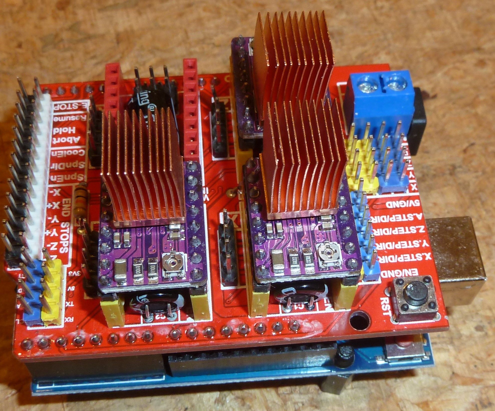
It makes for a permanent attachment, but from what I've read, this should allow them to be driven at their maximum rated current without overheating. This way I'll at least have a glimpse of what it's like to run the steppers at 45v with 2.1a current before switching over to the 24v volt closed loop drivers. I'll let the epoxy fully cure overnight and then give them a test drive tomorrow. It might (?) even turn out that with the extra power I don't even need the closed loop drivers. We'll see.I loaded GRBL 1.1h onto the arduino. Doing so is a very simple and quick process: just copy the GRBL library over to the arduino library folder and then compile and upload the uploadGRBL example program that comes with it. That's all there is to it. From there the default settings can be customized if so desired. I'll probably be testing different speed and acceleration settings.
-
@NeverDie Not surprisingly, some people are already doing laser ablation of soldermask, and the results are pretty good!
https://www.youtube.com/watch?v=tTKNvCmdWvc@NeverDie said in CNC PCB milling:
@NeverDie Not surprisingly, some people are already doing laser ablation of soldermask, and the results are pretty good!
https://www.youtube.com/watch?v=tTKNvCmdWvcI tried shopping for lasers last night, but it's not straight forward. The variables seem be: power, wavelength, focal distance, optics, size of dot, and sharpness of dot. Unfortunately, lasers don't seem to be marketed that way. Instead, the listings seem to assume you can infer that.
Apparently single mode lasers would be better for this application because they produce better defined dots, but that's the only tidbit of useful information I've so far gleaned. If anyone here with laser experience can make a recommendation for a CNC mountable laser to ablate solder mask, that would be great. Also, is it better to steer the beam by moving the laser around on the CNC as though it were and endmill, or is it better to get a laser with moveable mirrors to direct the beam where it should go? I'm guessing that treating it like an endmill would be the more plug-and-play of the two options, where you simply turn on the laser whenever the z-axis gcode implies the z-axis is below zero, and turn it off when the gcode implies the z-axis would be above zero. -
@NeverDie said in CNC PCB milling:
@NeverDie Not surprisingly, some people are already doing laser ablation of soldermask, and the results are pretty good!
https://www.youtube.com/watch?v=tTKNvCmdWvcI tried shopping for lasers last night, but it's not straight forward. The variables seem be: power, wavelength, focal distance, optics, size of dot, and sharpness of dot. Unfortunately, lasers don't seem to be marketed that way. Instead, the listings seem to assume you can infer that.
Apparently single mode lasers would be better for this application because they produce better defined dots, but that's the only tidbit of useful information I've so far gleaned. If anyone here with laser experience can make a recommendation for a CNC mountable laser to ablate solder mask, that would be great. Also, is it better to steer the beam by moving the laser around on the CNC as though it were and endmill, or is it better to get a laser with moveable mirrors to direct the beam where it should go? I'm guessing that treating it like an endmill would be the more plug-and-play of the two options, where you simply turn on the laser whenever the z-axis gcode implies the z-axis is below zero, and turn it off when the gcode implies the z-axis would be above zero.@NeverDie I could actually try this out.
I recently received solder mask paint, both white and green.
And I have a cheap 3 Chinese Watts uv laser engraver.
I was thinking that using transparent sheets is the easiest way to go since you have to expose it anyway, but ofcourse that also means more material use.
-
@NeverDie I could actually try this out.
I recently received solder mask paint, both white and green.
And I have a cheap 3 Chinese Watts uv laser engraver.
I was thinking that using transparent sheets is the easiest way to go since you have to expose it anyway, but ofcourse that also means more material use.
@Joerideman said in CNC PCB milling:
@NeverDie I could actually try this out.
I recently received solder mask paint, both white and green.
And I have a cheap UV laser engraver.
That would be great!
-
@NeverDie said in CNC PCB milling:
I suppose the GRBL capacitor rating may soon be a moot issue anyway, as the servo42A closed loop driver accepts an input voltage of only 12-24v, and, not surprisingly, it appears to have its own back EMF cap on its driverboard:

The original mechaduino v0.2 accepted up to 35v:
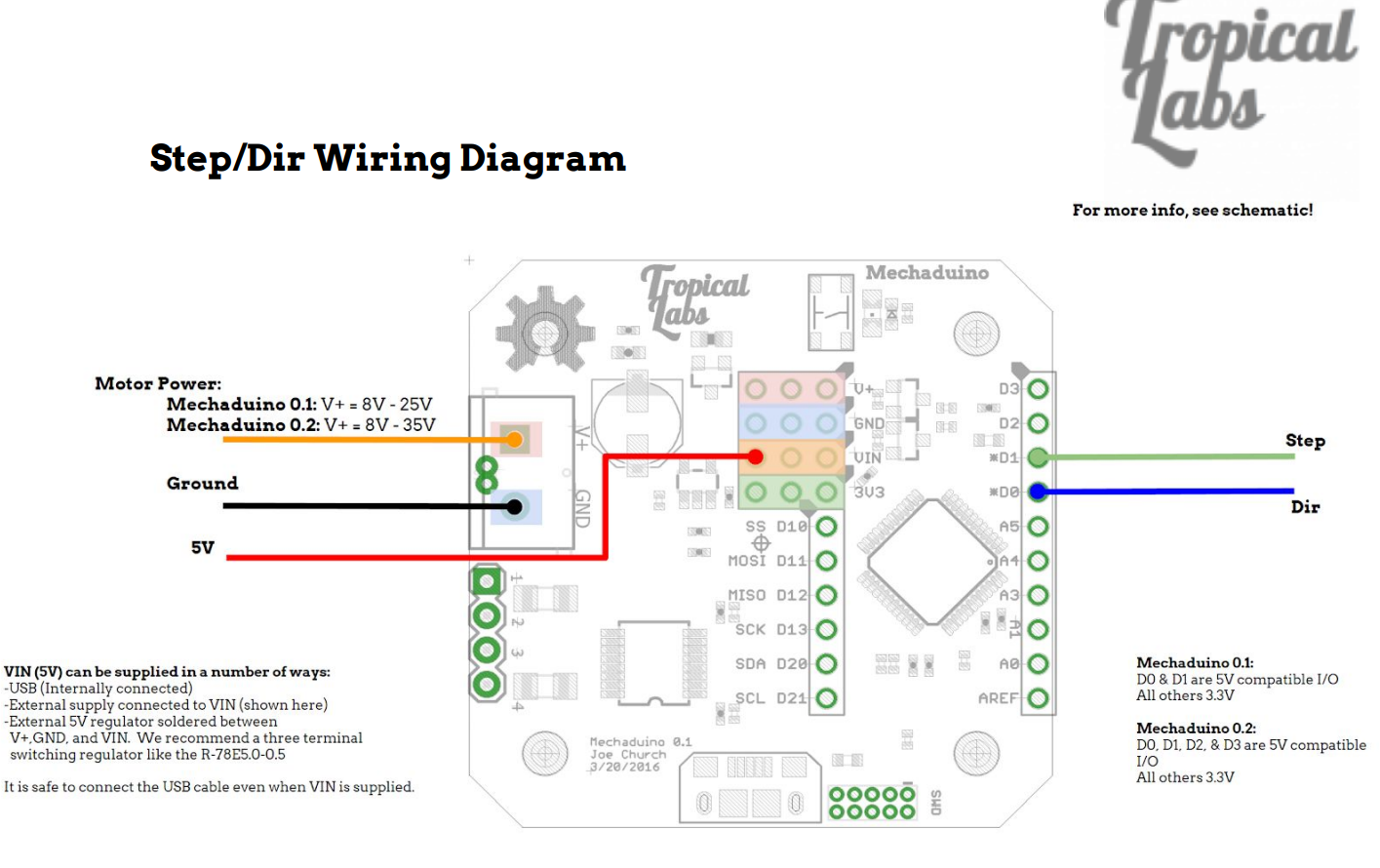
So, because the clone that I purchased allows for only 24v input, it's an unfortunate downgrade from the original. :(
@NeverDie said in CNC PCB milling:
@NeverDie said in CNC PCB milling:
I suppose the GRBL capacitor rating may soon be a moot issue anyway, as the servo42A closed loop driver accepts an input voltage of only 12-24v, and, not surprisingly, it appears to have its own back EMF cap on its driverboard:
The original mechaduino v0.2 accepted up to 35v:
So, because the clone that I purchased allows for only 24v input, it's an unfortunate downgrade from the original. :(
Reporting back: it turns out the voltage issue is moot. After playing around with a NEMA 17 and a DRV8255 driver, it turns out the NEMA 17 doesn't behave well at higher voltages anyway. At the higher voltages it's prone to resonating and not even turning. Also, unlike the original NEMA 17's, the "upgraded" NEMA 17's don't seem to perform well at 12v either. Rather, 24v seems to be more or less the sweet spot, and at a current that's around a little more half its rated maximum. So that was quite a surprise, at least to me. Also, even with the copper finned heatsinks, and the reduced voltages and currents, the DRV8255's get quite hot! If I'm going to run the upgraded steppers from stepsticks, I think I'm probably going to need to fan cooling in addition to the heatsinks. I wonder if I'll have to add some kind of heatsinks and fan cooling to the closed loop steppers as well?
I guess, if need be, I could either "downgrade" back to the original, smaller NEMA 17's that came with the kit, or else upgrade to TMC5160's (which run cooler) to better support the higher torque "upgraded" NEMA 17's. In the worst case I would shift to the standalone drivers discussed earlier, each of which comes with massive heatsinks.
All that said, the present currents are fairly paltry compared to what NEMA 23's consume. I imagine NEMA 23 drivers get very hot indeed!
Lastly, but importantly, I think I maybe see why my setup is loosing positioning when I jog around manually. Basically, by default GRBL turns off the drivers almost completely at the end of a command rather than maintaining holding torque on them. I'm guessing that may allow some slippage to happen that shouldn't happen during those relaxation periods. It has me curious now as to whether this might also happen while running a lengthy grbl script--maybe during periods when the z-height is locked and not otherwise changing? I guess I'll have to run some tests to find out. I find it hard to believe that GRBL might make a bonehead mistake like that, but.... maybe? Regardless, this would be something that the closed loop drivers could correct for, because their magnetic encoders have quite good resolution. :-) Based on tracking info, I'm pretty sure I'll be receiving them this week.
-
I never imagined that I would burn out four (4) DRV8825 stepper drivers and two (2) arduinos in just a short stretch of time. Something about this GRBL design makes it ridiculously fragile. And, by the way, the fuse never blew! :stuck_out_tongue_winking_eye: It really might as well be a piece of wire for all the good it's doing. I'm just glad it didn't fry the computer I have connected to it.
Edit: Good heavens! Here's a similar board, and beware! It's absolutely riddled with fatal flaws:
https://www.youtube.com/watch?v=U839EbPw-A8 -
I received the closed loop drivers. It contains a good amount of kit for making the upgrade:
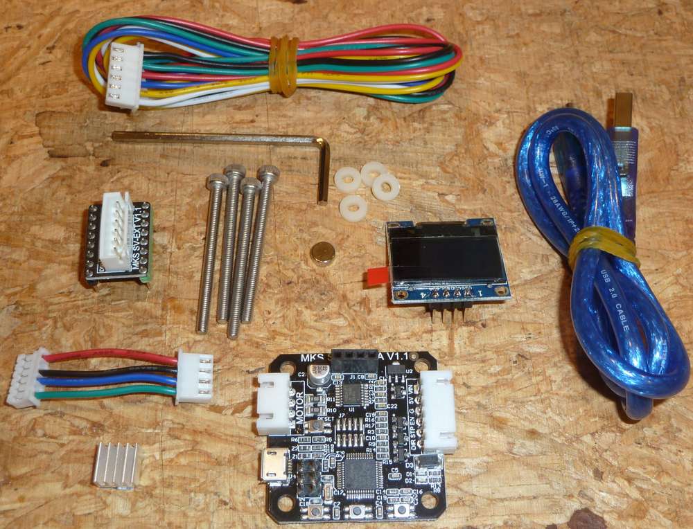
The board is missing the MCU programmer pins, so I presume the MCU is already programmed with at least a bootloader and most likely the full closed loop driver software.
-
@NeverDie I could actually try this out.
I recently received solder mask paint, both white and green.
And I have a cheap 3 Chinese Watts uv laser engraver.
I was thinking that using transparent sheets is the easiest way to go since you have to expose it anyway, but ofcourse that also means more material use.
@Joerideman said in CNC PCB milling:
@NeverDie I could actually try this out.
I recently received solder mask paint, both white and green.
And I have a cheap 3 Chinese Watts uv laser engraver.
I was thinking that using transparent sheets is the easiest way to go since you have to expose it anyway, but ofcourse that also means more material use.
While you're at it, would you please also try selectively curing the solder mask with your uv laser? If that could be done, I think it might be cleaner all around as compared to laser ablating solder mask that's already cured. For one thing, no fumes from burning to contend with. Also, I'm guessing the output power for curing could be less than for burning, and so maybe it would be safer to use for that reason.
On my end I found a 405nm laser on ebay with 600mw output power, with an adjustable focus, a focal length of 1 to 5 inches, and with a focus diameter of less than 100 microns. i.e. <0.01mm. I have no idea whether that's powerful enough to do laser ablation, but maybe?
Is there such a thing as solder mask which is clear to uv light? Anyone know? If not, then I'm guessing the solder mask would have to be applied very thinly, or else the uv light might not be able to penetrate deeply enough toe cure it all the way. So, for that reason, solder mask which is clear to uv light (even after curing) sounds like it would be the best, at least from a curing point of view. From a laser ablation point of view, I presume you would want just the opposite.
Edit: It turns out optically clear solder mask does exist. OSHPark uses it over their black FR4 substrate to create their "after dark" PCB's. Whether it is also clear to uv, though, I have no idea.
-
Hi all,
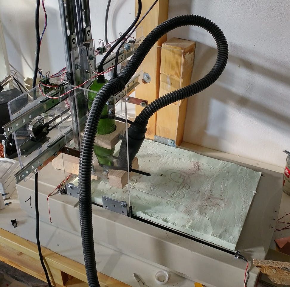
I build my CNC, to do PCB, i started from an old project and I add some addiction and I create the electronic with limit switch probe etc..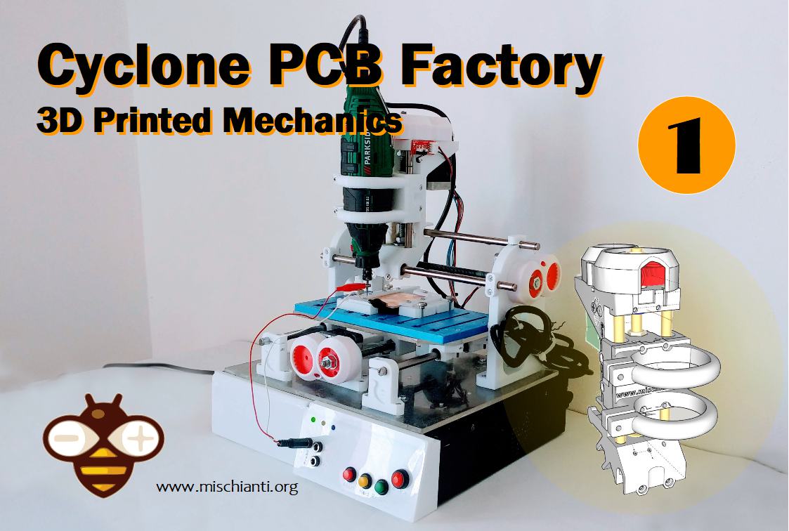
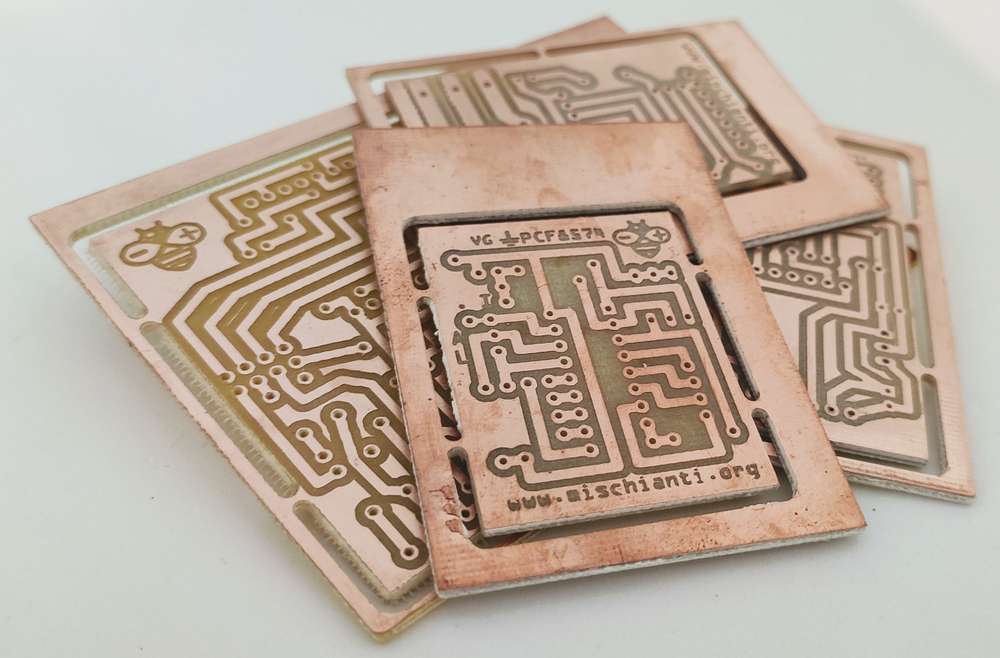
Here my tutorial to build 3D printed CNC
https://www.mischianti.org/category/tutorial/cyclone-pcb-factory-how-to-build-it/And Here the FlatCAM tutorial
https://www.mischianti.org/category/tutorial/flatcam-complete-tutorial/But my first CNC is in my heart :laughing: It's working, and I create a lot of PCB with that...
Naturally It's for home use, but I resolved a lot of situation with that.
Bye RM
-
@NeverDie 100 microns = 0.1mm 1m=1,000milimeters=1,000,000micrometers (microns) 1mm=1,000microns
The UV laser solder mask making has some issues:
- for curing with a laser you need a larger spot, imagine a 0.1mm beam scanning a whole 50x50mm pcb, that takes 500 passes to cover the whole board at 0.1mm resolution. A slightly out of focus laser with 0.3mm beam is more likely to get the job done faster and more uniform. To get the best results using cheap kinematics is best to "scan" the board with some margins for acceleration and deceleration, any attempt at vector cutting the shapes results in a lot of positional error due to backlash and slacks in the kinematics of these kind of laser.
- reflections, the stronger the uv the more it will flare and reflect and the reflections will cure adiacent regions, maybe some which should not get cured, a weak laser is preferred, 50mW or even less, to reduce flaring and reflections.
- burning away already cured paint.... I don't really know if it's possible, the UV paint is made to get cured by UV, not burned, you either need a very strong laser or a different wavelength, maybe CO2 laser. I happen to have a CO2 40W laser but never tried to burn already cured solder mask away.
- focusing and perpendicularity, a slightly not perpendicular beam has an oval shape and the vertical/horizontal size is thrown off, also slight height differences in substrate can and will make the focus spot bigger/smaller as the beam is a cone and you intersect it higher or lower.
LE. I would get an EleksMaker 405nm 500mw laser and start from there. https://www.banggood.com/EleksMaker-EL01-500-405nm-500mW-Blue-Violet-Laser-Module-PWM-Modulation-2_54-3P-DIY-Engraver-p-1287791.html?rmmds=search&cur_warehouse=CN
-
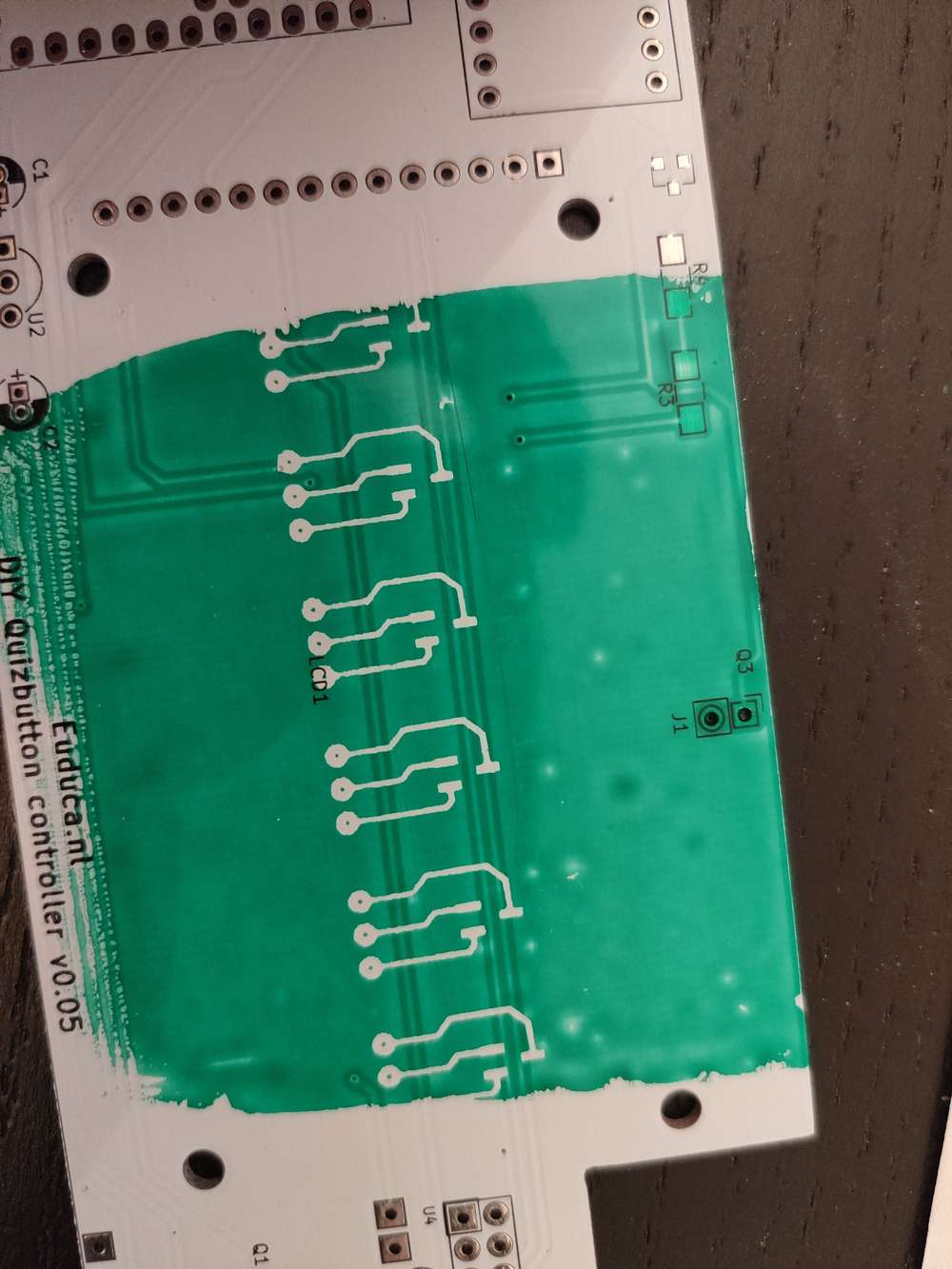
I just started with my first UV mask experience.
Following a YouTube video about how to apply the paint. I use a transparent sheet anyway to put the paint on. If I had printed the pads on there before exposing than my only task would have been to rinse it after a minute.
Either way, first test to apply it failed. Better cleaning next time.
So far... I find it difficult to apply the paint. And I find it difficult to expose the paint and then remove it again.
Edit: I have already reached the tenth test. So I am starting to root for the laser. although aligning will be very difficult.
Edit again: Exposing uv paint is problematic. It worked a bit, but I think I will have to experiment with curing times. It is far less forgiving than exposing pcb's. On the other hand... I now understand why they use there mill for this.
I am a bit out of material to put the paint on, and out of patience. The laser will have to come later. I am not so experienced yet using that thing. It takes a bit of time to set it up.
-
I just started with my first UV mask experience.
Following a YouTube video about how to apply the paint. I use a transparent sheet anyway to put the paint on. If I had printed the pads on there before exposing than my only task would have been to rinse it after a minute.
Either way, first test to apply it failed. Better cleaning next time.
So far... I find it difficult to apply the paint. And I find it difficult to expose the paint and then remove it again.
Edit: I have already reached the tenth test. So I am starting to root for the laser. although aligning will be very difficult.
Edit again: Exposing uv paint is problematic. It worked a bit, but I think I will have to experiment with curing times. It is far less forgiving than exposing pcb's. On the other hand... I now understand why they use there mill for this.
I am a bit out of material to put the paint on, and out of patience. The laser will have to come later. I am not so experienced yet using that thing. It takes a bit of time to set it up.
@Joerideman said in CNC PCB milling:
I just started with my first UV mask experience.
Following a YouTube video about how to apply the paint. I use a transparent sheet anyway to put the paint on. If I had printed the pads on there before exposing than my only task would have been to rinse it after a minute.
Either way, first test to apply it failed. Better cleaning next time.
So far... I find it difficult to apply the paint. And I find it difficult to expose the paint and then remove it again.
Edit: I have already reached the tenth test. So I am starting to root for the laser. although aligning will be very difficult.
Edit again: Exposing uv paint is problematic. It worked a bit, but I think I will have to experiment with curing times. It is far less forgiving than exposing pcb's. On the other hand... I now understand why they use there mill for this.
I am a bit out of material to put the paint on, and out of patience. The laser will have to come later. I am not so experienced yet using that thing. It takes a bit of time to set it up.
You might want to try a drawdown bar to get a precise, uniform, and repeatable (!) film thickness:

There are different types of coating bars. Some have adjustable heights. They all work on the same principle. You'd have to account for the height of your PCB, instead of the height of paper or a drawdown card, but aside from that it should work the same. They are essentially screeds. You probably want to aim for a thickness above the copper of about 0.5mm. I've seen youtube videos where people try to achieve that by just eyeballing it, but good luck with that.
-
Hi all,
I build my CNC, to do PCB, i started from an old project and I add some addiction and I create the electronic with limit switch probe etc..
Here my tutorial to build 3D printed CNC
https://www.mischianti.org/category/tutorial/cyclone-pcb-factory-how-to-build-it/And Here the FlatCAM tutorial
https://www.mischianti.org/category/tutorial/flatcam-complete-tutorial/But my first CNC is in my heart :laughing: It's working, and I create a lot of PCB with that...
Naturally It's for home use, but I resolved a lot of situation with that.
Bye RM
@Renzo-Mischianti Thanks for your post. Looks like you've been quite a busy bee. ;-)
Have you had any success with solder mask? -
@Joerideman said in CNC PCB milling:
I just started with my first UV mask experience.
Following a YouTube video about how to apply the paint. I use a transparent sheet anyway to put the paint on. If I had printed the pads on there before exposing than my only task would have been to rinse it after a minute.
Either way, first test to apply it failed. Better cleaning next time.
So far... I find it difficult to apply the paint. And I find it difficult to expose the paint and then remove it again.
Edit: I have already reached the tenth test. So I am starting to root for the laser. although aligning will be very difficult.
Edit again: Exposing uv paint is problematic. It worked a bit, but I think I will have to experiment with curing times. It is far less forgiving than exposing pcb's. On the other hand... I now understand why they use there mill for this.
I am a bit out of material to put the paint on, and out of patience. The laser will have to come later. I am not so experienced yet using that thing. It takes a bit of time to set it up.
You might want to try a drawdown bar to get a precise, uniform, and repeatable (!) film thickness:
There are different types of coating bars. Some have adjustable heights. They all work on the same principle. You'd have to account for the height of your PCB, instead of the height of paper or a drawdown card, but aside from that it should work the same. They are essentially screeds. You probably want to aim for a thickness above the copper of about 0.5mm. I've seen youtube videos where people try to achieve that by just eyeballing it, but good luck with that.
@NeverDie for lack of such a roll I have tried another idea I found on YouTube.
I used my laminator to spread out the paint. It gives not that perfect result that you see on factory prints but I was able to expose it for 30s and then a minute of cleaning and then another 2 minutes of exposing.
It is a very solid and well formed layer. Very scratch resistant.
I will have another go on the other side to see if this is repeatable.
Edit:
This is very repeatable. I tried scrubbing with alcohol first but aceton might be a bit better.
The letters are less than 0,4mm wide.
After scrubbing I exposed everything for another 3 minutes and than it seems to be scratch resistant.
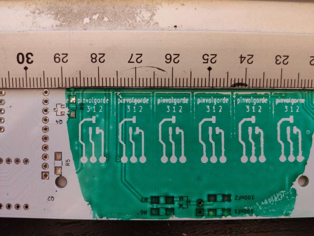
So while I have not yet tested laser exposure or laser engraving, I have now tested a potential reliable way of applying the paint.
-
@NeverDie for lack of such a roll I have tried another idea I found on YouTube.
I used my laminator to spread out the paint. It gives not that perfect result that you see on factory prints but I was able to expose it for 30s and then a minute of cleaning and then another 2 minutes of exposing.
It is a very solid and well formed layer. Very scratch resistant.
I will have another go on the other side to see if this is repeatable.
Edit:
This is very repeatable. I tried scrubbing with alcohol first but aceton might be a bit better.
The letters are less than 0,4mm wide.
After scrubbing I exposed everything for another 3 minutes and than it seems to be scratch resistant.
So while I have not yet tested laser exposure or laser engraving, I have now tested a potential reliable way of applying the paint.
@Joerideman Looks promising.
What is it that you put down on top of the solder mask before putting it into the laminator? I guess some kind of acetate with a black uv mask printed on it?
How many passes through the laminator?
-
@Joerideman said in CNC PCB milling:
I just started with my first UV mask experience.
Following a YouTube video about how to apply the paint. I use a transparent sheet anyway to put the paint on. If I had printed the pads on there before exposing than my only task would have been to rinse it after a minute.
Either way, first test to apply it failed. Better cleaning next time.
So far... I find it difficult to apply the paint. And I find it difficult to expose the paint and then remove it again.
Edit: I have already reached the tenth test. So I am starting to root for the laser. although aligning will be very difficult.
Edit again: Exposing uv paint is problematic. It worked a bit, but I think I will have to experiment with curing times. It is far less forgiving than exposing pcb's. On the other hand... I now understand why they use there mill for this.
I am a bit out of material to put the paint on, and out of patience. The laser will have to come later. I am not so experienced yet using that thing. It takes a bit of time to set it up.
You might want to try a drawdown bar to get a precise, uniform, and repeatable (!) film thickness:
There are different types of coating bars. Some have adjustable heights. They all work on the same principle. You'd have to account for the height of your PCB, instead of the height of paper or a drawdown card, but aside from that it should work the same. They are essentially screeds. You probably want to aim for a thickness above the copper of about 0.5mm. I've seen youtube videos where people try to achieve that by just eyeballing it, but good luck with that.
@NeverDie said in CNC PCB milling:
You probably want to aim for a thickness above the copper of about 0.5mm
Correction: I should have said 0.5 mils.
That's according to altium: https://resources.altium.com/p/how-choose-correct-solder-mask-your-pcb#:~:text=The typical solder mask thickness,solder mask over your traces.
However, I'm not sure if they're referring to wet film thickness or dry film thickness. I guess with uv cured paint it maybe would be the same either way?