Everything nRF52840
-
@NeverDie That's right. You may want to use open version which is much smaller indeed.
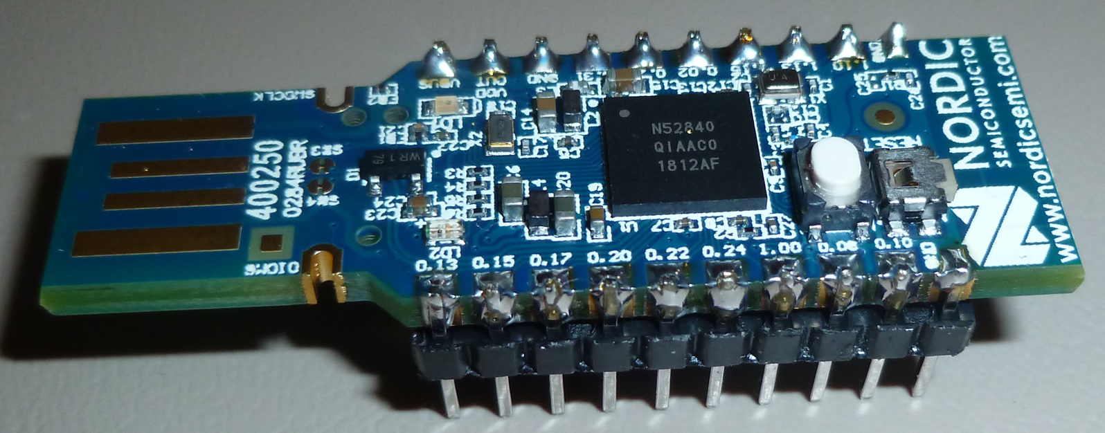
Also, for nRF52 only three pins are required: SWDIO, SWDCLK, and VTref. All the three are very conveniently located in close proximity on pins 2, 4 and 1:
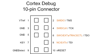
Such, for a tiny custom board a 2x2 pin header, 1.27 pitch can be used w/o breaking compatibility.
@Mishka How about this?
https://www.amazon.com/CQRobot-Programmer-Testing-Support-Programmer/dp/B07BWFJL31Either 4 pads on one side or 2 pads on each side of the PCB. Very inexpensive. Not sure if they make a 4 pin clip, but if so, that would be ideal.
Maybe if instead of pads you went for 4 through-holes it would even self-align?
-
This is quite clever:
https://www.youtube.com/watch?v=xgLEhTSYqL4If you simply stagger the through-holes then a regular block of header pins will fit through and hold itself in place. No pogo pins required.
-
This is quite clever:
https://www.youtube.com/watch?v=xgLEhTSYqL4If you simply stagger the through-holes then a regular block of header pins will fit through and hold itself in place. No pogo pins required.
@NeverDie said in Everything nRF52840:
If you simply stagger the through-holes then a regular block of header pins will fit through and hold itself in place. No pogo pins required.
I'm not so sure about the reliability of this ... It's not very difficult to make an adapter using pogo pins, you just need to use 2 similar pcbs to align them properly.
Another option is to use smaller headers (2mm or better 1.27 mm) and an adapter from selected spacing to 2.54mm header: cheap and compact connector for the board, cheap adapter and reliable connection.
For example on these adapters you can solder a SMD header on the 1.27mm spaced side and have 2.54mm connectors. You just need to have the opposite genre 1.27mm header on the board and you're done.
https://www.aliexpress.com/item/32855731928.html -
@Mishka How about this?
https://www.amazon.com/CQRobot-Programmer-Testing-Support-Programmer/dp/B07BWFJL31Either 4 pads on one side or 2 pads on each side of the PCB. Very inexpensive. Not sure if they make a 4 pin clip, but if so, that would be ideal.
Maybe if instead of pads you went for 4 through-holes it would even self-align?
@NeverDie
There is an article on hackaday about this type of clamp that even has a KiCAD footprint. I bought one of the clips, but haven't tried it out yet.
https://hackaday.io/project/165917-soicbite-programmingdebug-connector-footprintI also tried this one from Adafruit;
https://www.adafruit.com/product/4048
small, jlink-mini compatible, and polarized.So far, my preferrred solution is a 6 pin jst-sh connector.
small. 3v3, gnd, swdio, swclk, tx, rx
and polarized.My old eyes get tired of confirming I have the pins on in the right direction. Polarization is really nice.
-
@NeverDie said in Everything nRF52840:
If you simply stagger the through-holes then a regular block of header pins will fit through and hold itself in place. No pogo pins required.
I'm not so sure about the reliability of this ... It's not very difficult to make an adapter using pogo pins, you just need to use 2 similar pcbs to align them properly.
Another option is to use smaller headers (2mm or better 1.27 mm) and an adapter from selected spacing to 2.54mm header: cheap and compact connector for the board, cheap adapter and reliable connection.
For example on these adapters you can solder a SMD header on the 1.27mm spaced side and have 2.54mm connectors. You just need to have the opposite genre 1.27mm header on the board and you're done.
https://www.aliexpress.com/item/32855731928.html@Nca78 Yup, I too would worry a bit about the long-term repeatability of the staggered pin approach: after you hook it up a few times, maybe the metal on the throughhole would have scraped off due to the friction fit?
I was thinking that on an "as small as possible" type of board like on Mishka's current project that the castellated connection would have the smallest footprint. On a larger board where space doesn't matter, then, yeah, I would go for some kind of pinned connection. For instance, on my 10 year motion detector, the board size is huge due to just the batteries, so there is plenty of free space to plunk down a connector:
https://www.openhardware.io/view/499/10-years-wireless-PIR-Sensor-on-just-one-set-of-3-AAs
Yet, when it came to mount it in a case, that connector got in the way, and I had to redesign it to use the usb connector that everybody but me seemed to hate on the backside, fitted between the batteries. I suppose I could have used some kind of edge pin connector though if it were small enough.
It would be fun to make a board the same dimensions as an esp8266 or esp32 or wroom module so that I could use one of the test/burner jigs that's designed for them to make the castellated edge connections.
-
@NeverDie
There is an article on hackaday about this type of clamp that even has a KiCAD footprint. I bought one of the clips, but haven't tried it out yet.
https://hackaday.io/project/165917-soicbite-programmingdebug-connector-footprintI also tried this one from Adafruit;
https://www.adafruit.com/product/4048
small, jlink-mini compatible, and polarized.So far, my preferrred solution is a 6 pin jst-sh connector.
small. 3v3, gnd, swdio, swclk, tx, rx
and polarized.My old eyes get tired of confirming I have the pins on in the right direction. Polarization is really nice.
@nagelc said in Everything nRF52840:
There is an article on hackaday about this type of clamp that even has a KiCAD footprint. I bought one of the clips, but haven't tried it out yet.
https://hackaday.io/project/165917-soicbite-programmingdebug-connector-footprintI couldn't find where to buy that soic bite. Is it even for sale anymore?
-
On the other hand, the JST-XSR connector might not be a bad way to go. At 0.6mm pitch, a 4 wire connector is just 3mm wide:
http://www.jst-mfg.com/product/pdf/eng/eXSR.pdf?5e312adac5a05
It's seems very hard to find for sale though.AFAIK, it's the smallest jst connector there is.
-
@nagelc said in Everything nRF52840:
There is an article on hackaday about this type of clamp that even has a KiCAD footprint. I bought one of the clips, but haven't tried it out yet.
https://hackaday.io/project/165917-soicbite-programmingdebug-connector-footprintI couldn't find where to buy that soic bite. Is it even for sale anymore?
@NeverDie I don't think that SOICbite has ever been sold. It's just a conventional SOIC-8 test clip, that may need some modification, like filing away some of the plastic in front of the hinge or at the tip. I like the idea of this method because, apart from having a small footprint, they are super cheap (even less than 2 USD/EUR incl. shipping from China, like this one) and it doesn't require additional parts for every single PCB for a one-time job.
I'm currently designing a PCB (not nRF52840-related though) with the SOICbite connector on it and have some clips on order, to see how well it works. Might take a while until I reveice them, but I can report back as soon as I tested them.
-
hey guys. I'm testing couple of nrf52840 modules. so far i was able to test raytac mdbt50q ipex and e73-2G4M08S1C modules with basic rssi value.
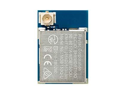
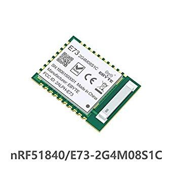 so far ipex version looks abit better but at a cost of external cable and antenna where e73-2G4M08S1C is compact and difference is not that significant.
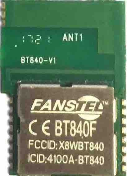
i later saw fanstel products, particularly interested in BT840F model because reported range is significantly better than the BT840 model and the only difference is the antenna design between them.
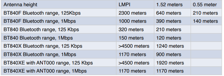
Considering this difference 840F might be way better than the e73-2G4M08S1C. Has anyone able to compare them or test them directly? -
hey guys. I'm testing couple of nrf52840 modules. so far i was able to test raytac mdbt50q ipex and e73-2G4M08S1C modules with basic rssi value.
so far ipex version looks abit better but at a cost of external cable and antenna where e73-2G4M08S1C is compact and difference is not that significant.
i later saw fanstel products, particularly interested in BT840F model because reported range is significantly better than the BT840 model and the only difference is the antenna design between them.
Considering this difference 840F might be way better than the e73-2G4M08S1C. Has anyone able to compare them or test them directly?@orhanyor I compared the Fanstel BT840F to the Ebyte with the trace antenna, and the Fanstel was better. I expect the trace anenna is better than the chip antenna on the module that you referred to, so by the transitive property of inequality, I expect the Fanstel would be better than it.
-
@orhanyor I compared the Fanstel BT840F to the Ebyte with the trace antenna, and the Fanstel was better. I expect the trace anenna is better than the chip antenna on the module that you referred to, so by the transitive property of inequality, I expect the Fanstel would be better than it.
@NeverDie thanks for the reply i hope to try them in the future. Best option is definitely something like BT840X or another nrf52840 or 32 with PA/LNA module it needs to be implemented with a code. i found this https://devzone.nordicsemi.com/nordic/nordic-blog/b/blog/posts/pa-lna-support-in-s132 in nordic forums but im not sure how it can be implemented into an arduino environment.
I actually added this code to an arduino sketch and it compiled without an issue but I cant tell if it will work without having a module with PA. -
@orhanyor I compared the Fanstel BT840F to the Ebyte with the trace antenna, and the Fanstel was better. I expect the trace anenna is better than the chip antenna on the module that you referred to, so by the transitive property of inequality, I expect the Fanstel would be better than it.
@NeverDie also according to this post when TX/RX pins are defined softdevice handles them automatically. https://devzone.nordicsemi.com/f/nordic-q-a/40504/nrf52840-and-pa
But if you have more control in your FEM like in BT840X with SKY66112 you need to control 2-3 more pins in your code. nRF24 modules mostly use RFX2401C its quite simple with only TX/RX pins and it works quite well may be it will pair nicely with nrf52 modules only if we could configure the code for arduino. -
I also designed this 2 layer breakout board with a much bigger inverted F antenna design for the nrf52840, ive put BT840 to compare the antenna size. (still needs some touch ups here and there)
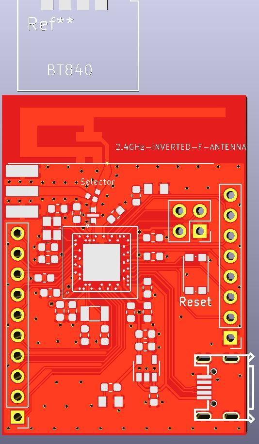
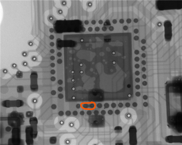
bottom layer has a good ground layer for the antenna and i believe its going to perform better but just to be sure theres a SMA option for external antenna aswell which can be selected with the 0 ohm resistor.
nordic specialist approved it and i will probably give it a try just to compare the antenna performance. My only concern is how hard soldering is going to be. if you noticed i removed the pins who are next to each other(i left some because they are mandatory like d+ - swclk etc..) and left the diagonal ones in order to reduce the chance of possible solder bridges. as you can see from the picture there are reports about solder bridges detected with expensive xray machines which i dont have :) so, fewer the pin count less probability for failure.
on the other hand ebyte nrf52840 e73 modules even with the bottom pads are really easy to solder without a probability to bridge anything and cause issues because bottom pad to pad distance is very generous, im really happy with that.
-
I also designed this 2 layer breakout board with a much bigger inverted F antenna design for the nrf52840, ive put BT840 to compare the antenna size. (still needs some touch ups here and there)
bottom layer has a good ground layer for the antenna and i believe its going to perform better but just to be sure theres a SMA option for external antenna aswell which can be selected with the 0 ohm resistor.
nordic specialist approved it and i will probably give it a try just to compare the antenna performance. My only concern is how hard soldering is going to be. if you noticed i removed the pins who are next to each other(i left some because they are mandatory like d+ - swclk etc..) and left the diagonal ones in order to reduce the chance of possible solder bridges. as you can see from the picture there are reports about solder bridges detected with expensive xray machines which i dont have :) so, fewer the pin count less probability for failure.
on the other hand ebyte nrf52840 e73 modules even with the bottom pads are really easy to solder without a probability to bridge anything and cause issues because bottom pad to pad distance is very generous, im really happy with that.
@orhanyor Beautiful work, but how exactly do you manage to solder it? I wouldn't know how to even align it properly without some sort of jig to plunk the nRF52840 down. I'm not sure that even a surgeon at the top of his game would have the needed manual dexterity. There must be some tricks to doing this right that the module makers use. I'd think you'd have to get at least reasonably close in the first place for the surface tension of the melted lead to pull things into place.
-
@orhanyor Beautiful work, but how exactly do you manage to solder it? I wouldn't know how to even align it properly without some sort of jig to plunk the nRF52840 down. I'm not sure that even a surgeon at the top of his game would have the needed manual dexterity. There must be some tricks to doing this right that the module makers use. I'd think you'd have to get at least reasonably close in the first place for the surface tension of the melted lead to pull things into place.
@NeverDie soldering bottom/non visible parts needs at least some sort of reflow oven to make sure they melt and make connection. checking for bridges tho is impossible with microscope etc because they are under the chip. diagonal pin pitch is at around 0.55 and the ones on the same row are at 0.5 which is normal qfn package. if you can solder qfn package this is not a problem but the hardest thing is inability of inspection at hobbyist level :)
aligning is very simple, you just need to have correct courtyard printed on the silk layer of the pcb for the chip/module so when you place the chip/module on to the pcb, it needs to sit exactly on top of the courtyard drawing on the silk layer then you know your pads are exactly where they need to be.
sadly tho bigger parts like these modules cant benefit from the surface tension force is not enough to pull the weight but then again its very hard to misplace them especially the e73 module. raytac modules(blue one in the picture) are hard aswell they are like super tiny :) heres how it is under the chip but it baked nicely and it works as expected.
i hope to solder aQFN package aswell but im really not sure about that one :)) standard QFN with visible pads on the side is very nice i wish nrf52840 was like that.
-
@NeverDie soldering bottom/non visible parts needs at least some sort of reflow oven to make sure they melt and make connection. checking for bridges tho is impossible with microscope etc because they are under the chip. diagonal pin pitch is at around 0.55 and the ones on the same row are at 0.5 which is normal qfn package. if you can solder qfn package this is not a problem but the hardest thing is inability of inspection at hobbyist level :)
aligning is very simple, you just need to have correct courtyard printed on the silk layer of the pcb for the chip/module so when you place the chip/module on to the pcb, it needs to sit exactly on top of the courtyard drawing on the silk layer then you know your pads are exactly where they need to be.
sadly tho bigger parts like these modules cant benefit from the surface tension force is not enough to pull the weight but then again its very hard to misplace them especially the e73 module. raytac modules(blue one in the picture) are hard aswell they are like super tiny :) heres how it is under the chip but it baked nicely and it works as expected.
i hope to solder aQFN package aswell but im really not sure about that one :)) standard QFN with visible pads on the side is very nice i wish nrf52840 was like that.
@orhanyor Ah, I see now.
I wonder if you could use through-holes to gain access to the pads on the back of the module? I ended up doing that on one of my energy harvester boards to solder a ground pad that was on the back of a chip:
https://www.openhardware.io/view/733/Buck-Energy-Harvester
It worked, but it was a simpler case. In your case maybe you'd have to cut channels instead of holes. -
@orhanyor Ah, I see now.
I wonder if you could use through-holes to gain access to the pads on the back of the module? I ended up doing that on one of my energy harvester boards to solder a ground pad that was on the back of a chip:
https://www.openhardware.io/view/733/Buck-Energy-Harvester
It worked, but it was a simpler case. In your case maybe you'd have to cut channels instead of holes.@NeverDie yes that is definitely an option ive seen people do it with normal thru holes on those pads and it works. you might wanna pre tin the pads of the module and its good to go but good news for the E73(ebyte) module specifically none of the bottom pads are necessary for the module to work. they mapped every mandatory pin to the edge of the module which is very hobbyist friendly but of course you will have very few gpio pins to work with but still its very well thought by ebyte.
i dont know when i will order the pcb for the nrf52840 but i will definitely report the result and the antenna performance :) i also want to use this antenna for nrf24 but yea it is gonna have to wait not in a hurry atm. -
@NeverDie yes that is definitely an option ive seen people do it with normal thru holes on those pads and it works. you might wanna pre tin the pads of the module and its good to go but good news for the E73(ebyte) module specifically none of the bottom pads are necessary for the module to work. they mapped every mandatory pin to the edge of the module which is very hobbyist friendly but of course you will have very few gpio pins to work with but still its very well thought by ebyte.
i dont know when i will order the pcb for the nrf52840 but i will definitely report the result and the antenna performance :) i also want to use this antenna for nrf24 but yea it is gonna have to wait not in a hurry atm.@orhanyor I'm very interested in your results. I think you may be the first to upgrade a module antenna. It might save a lot of money if cheaper modules can be used. Fanstells are pricey for their good antenna, so if your approach is just as good or even better...
-
@orhanyor I'm very interested in your results. I think you may be the first to upgrade a module antenna. It might save a lot of money if cheaper modules can be used. Fanstells are pricey for their good antenna, so if your approach is just as good or even better...
@NeverDie price wise i think e73 modules are unbeatable they are 3.. dollar or something with the current discount in aliexpress. just for the nrf52840 Soc price in mouser is $5.5 which is still ok if theres going to be a noticeable difference in signal strength. considering much bigger ground plane and bigger antenna i expect better performance but need to test it :) aside from the soc theres a low pass filter which is .30 and a crystal which is probably around .20-.30
that blue raytac module was https://www.raytac.com/product/ins.php?index_id=24 8 or $9 which gave almost the same performance as the e73 so at that price point ive not tested it but BT840F($7) looks better and much easier to solder as the bottom pin pitch is whooping 1.5mm or so.. you can park a truck between those pins :)) -
To free up this thread for its primary purpose, I just now started a new thread for anyone wanting to continue the wristwatch topic: https://forum.mysensors.org/topic/10917/wristwatches-that-invite-development