💬 Adjustable Boost Converter with Pass-Through
-
The problem for me is that this is suddenly a lot more work than I had planned on. I have about 8 different booster chips I was planning to brute force try to see which worked best in the application. If I have to create stringent patterns for each just in order to try them, it's going to exceed the time I had budgeted for this. So, I'm going to put this on hold.
I've already ordered the boards that I had posted. I'll try them out after receiving them. Maybe some of them will work well enough to proceed from there, or at least narrow down the list of candidates for which I create more detailed patterns. Anyhow, thanks for the input. At least if they aren't working as expected I'll have some idea as to why. One of the chips has built in MPPC, and so I might just focus on that one, as it really is intended for a solar application.
-
oki ;)
i also have designed multiple eval boards..too much stuff to release, but sure i could release some. that shoule be quick job. i have boosters, buck, boost/buck, solar etc.. :smile:Here is a pic of my eval board for MCP1640, i did it a while ago when i did my ulpnode..
-
oki ;)
i also have designed multiple eval boards..too much stuff to release, but sure i could release some. that shoule be quick job. i have boosters, buck, boost/buck, solar etc.. :smile:Here is a pic of my eval board for MCP1640, i did it a while ago when i did my ulpnode..
-
oki ;)
hopefully this is quick stuff, because i have an avalanche of stuff to release! and still some non complete release to clean..that's always the same i'm lazy boy, i prefer to play :) -
Interestingly, the datasheet for the LTC3105 boost converter with the built-in MPPC does not make any reference to a recommended trace or component layout: http://cds.linear.com/docs/en/datasheet/3105fb.pdf That's in contrast to most of the other boost converters, which do. Since it does not appear to be burdened by layout restrictions, I'll throw together a board for that and post it. Also, if I'm reading it right, it does not appear to require the use of a blocking diode to prevent the current from discharging back through the PV cell under low light conditions, which if true, is also nice.
That said, I'll change the layout strategy to at least put the capacitors at a shorter distance to the chip. On the boards I had already posted, I had put them on the back so as to keep the board size as small as possible (and thereby fab costs low). So, the board may need to grow a little bigger to keep the caps on the same layer as the chip, but I guess that's probably par for the course.
-
If you ask me, chip manufacturers should publish the PCB (gerber files, etc.) for their "typical" application circuit. It would save me from having to re-invent it just so I can take their chip for a test drive. As it stands, you have to buy their costly "evaluation boards"--or else go to the effort of creating your own--to help decide if you might want to possibly use their chip. It should be in their interest to make it as easy as possible for people to test drive their chips. What's the point in getting free sample chips if you have to create a PCB from scratch and wait two weeks for fabrication just to try it out? It makes no sense. Am I missing something?
@NeverDie said:
If you ask me, chip manufacturers should publish the PCB (gerber files, etc.) for their "typical" application circuit. It would save me from having to re-invent it just so I can take their chip for a test drive. As it stands, you have to buy their costly "evaluation boards"--or else go to the effort of creating your own--to help decide if you might want to possibly use their chip. It should be in their interest to make it as easy as possible for people to test drive their chips. What's the point in getting free sample chips if you have to create a PCB from scratch and wait two weeks for fabrication just to try it out? It makes no sense. Am I missing something?
After reflecting on this question, I'm guessing that most EE's probably use a spice simulator, or similar CAD tool, for designing and testing their circuits. So, for them, having the physical chip itself isn't so important. Maybe I should look into doing the same.
-
To expedite things, I just now posted Version 2:
- I re-did the routing placement to make it conform with the recommendations, and
- I cleaned up the silkscreen to make the component labels more legible.
-
I just now posted Version 3.
Changes from Version 2:
- Change to using the same type of shielded inductor that my other boost projects are using.
- Eliminated unnecessary header pins, and added a ground header pin.
- Changed the silkscreen on the MCP1640 land pattern to mitigate against potential for solder bridging.
-
I've tested the board, and it works.
Please purchase your PCB's for this project from the following link: https://pcbs.io/share/zyLW7
-
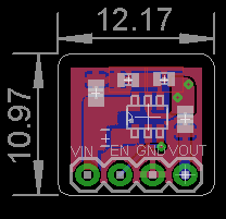
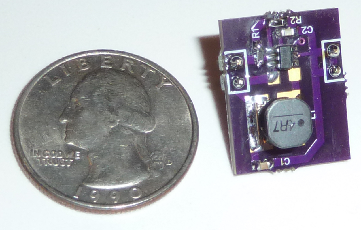
Here is a photo of the assembled PCB, taken next to a quarter for scale:
-
This project is now finished. :smile:
-
Setting R1=680K gives a voltage output of 2.674v, which is great for charging 2.7v supercaps.
-
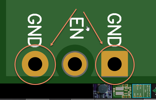
I just now revised the board to expose the Enable pin, so now you can do a pass-through if you wish. I also made it more compact and gave it a ground-plane on the back. Enjoy!
-
i received the upgraded PCB and assembled it. It tests out correctly. The project photo now shows the newest board. Project completed. :)
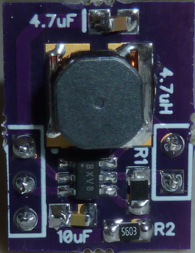
For 3.3v output, use R1=976 ohms and R2=562 ohms, as per the datasheet.
-
i received the upgraded PCB and assembled it. It tests out correctly. The project photo now shows the newest board. Project completed. :)
For 3.3v output, use R1=976 ohms and R2=562 ohms, as per the datasheet.
BTW, the same PCB and circuit can also be used with the MCP1640T instead of the MCP1640C if so desired. In that case, the ENABLE pin acts like an ON/OFF switch, instead of an ON/Pass-through switch.
-
Just little tip from me :) Use thermal relief instead of direct polygon connection.
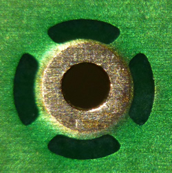
It is much more useful in such cases. -
Just little tip from me :) Use thermal relief instead of direct polygon connection.
It is much more useful in such cases.@Koresh said in 💬 Adjustable Boost Converter with Pass-Through:
Just little tip from me :) Use thermal relief instead of direct polygon connection.
It is much more useful in such cases.Where do I put that exactly?
-
@Koresh said in 💬 Adjustable Boost Converter with Pass-Through:
Just little tip from me :) Use thermal relief instead of direct polygon connection.
It is much more useful in such cases.Where do I put that exactly?
-
Sorry if I'm being dense, but how are the thermal reliefs better? What's their advantage?
-
Sorry if I'm being dense, but how are the thermal reliefs better? What's their advantage?
@NeverDie It is much easier to solder the wire to pads with relief connection than the wire to directly connected pads. Your soldering point even can be unreliable if your pad is directly connected to very huge polygon and your soldering iron don't have enough power.
Hello! It looks like you're interested in this conversation, but you don't have an account yet.
Getting fed up of having to scroll through the same posts each visit? When you register for an account, you'll always come back to exactly where you were before, and choose to be notified of new replies (either via email, or push notification). You'll also be able to save bookmarks and upvote posts to show your appreciation to other community members.
With your input, this post could be even better 💗
Register Login