Easy/Newbie PCB for MySensors
-
@helvetian - just so you dont miss this. A Atmega328 (Pro mini if you are using EasyPCB) can be run without a booster by reprogramming the fuses/bootloader. This is more advanced but possible. Then you can run the pro mini with a 8mhz or 1mhz internal clock down to the radio minimum 1.9v. This is a better option compared to boosters but harder to achieve.
@sundberg84 said in Easy/Newbie PCB for MySensors:
@helvetian - just so you dont miss this. A Atmega328 (Pro mini if you are using EasyPCB) can be run without a booster by reprogramming the fuses/bootloader. This is more advanced but possible. Then you can run the pro mini with a 8mhz or 1mhz internal clock down to the radio minimum 1.9v. This is a better option compared to boosters but harder to achieve.
No it is not "hard". You just need to copy files in a directory, edit a text file and flash ISP sketch on a nano or uno bard. Easier than dealing with unreliable boosters :p
-
@sundberg84 said in Easy/Newbie PCB for MySensors:
@helvetian - just so you dont miss this. A Atmega328 (Pro mini if you are using EasyPCB) can be run without a booster by reprogramming the fuses/bootloader. This is more advanced but possible. Then you can run the pro mini with a 8mhz or 1mhz internal clock down to the radio minimum 1.9v. This is a better option compared to boosters but harder to achieve.
No it is not "hard". You just need to copy files in a directory, edit a text file and flash ISP sketch on a nano or uno bard. Easier than dealing with unreliable boosters :p
@nca78 ... can be discussed. Wiring needs to be right. It's not hard when you know what to do but it's harder compared to a working booster.
Controller: Proxmox VM - Home Assistant
MySensors GW: Arduino Uno - W5100 Ethernet, Gw Shield Nrf24l01+ 2,4Ghz
MySensors GW: Arduino Uno - Gw Shield RFM69, 433mhz
RFLink GW - Arduino Mega + RFLink Shield, 433mhz -
@nca78 ... can be discussed. Wiring needs to be right. It's not hard when you know what to do but it's harder compared to a working booster.
-
@gohan - sorry, didnt understand?
-
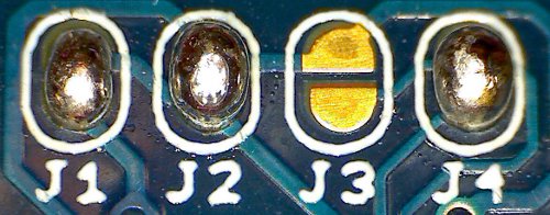
I've just built a few nodes using the EasyPCB Rev 9 RFM69 Edition and I can confirm it lives up to its name - build takes only 15-20 mins, and node works first time because there is no chance of incorrectly wiring the radio. Thanks @sundberg84!
The PCB fits nicely along with 1 or 2 AA batteries into the 100x60x25 project boxes available on eBay for about $1 each:
(AA battery holder is actually about 1.5mm too long to fit - I've cut off the non-spring end of the holder, and the positive wire is held by tension between the +ve battery terminal and the side of the case. Ugly, but fine for nodes that don't get moved around. White tape is to prevent antenna from shorting against the top of the radio module.)
I have a couple of observations that might be worth considering to make the next revision even better:
- According to the MySX specification, MySX header pin 10 should be connected to Arduino pin D4, not D2 (which is already used for the radio)?
- It would be handy to have a bit more space between the voltage booster and the adjacent cap - boosters with pre-soldered right-angle headers don't fit without hiting the adjacent cap (see photo). You could free up some space for this by mounting the battery measurement resistors vertically. (There is a risk that this might cause the voltage divider circuit to pick up noise from the adjacent booster; which might cause a bit of random fluctuation in the battery voltage readings. I suppose you'd need to do some tests to see if this is actually an issue.)
- I put a few layers of insulating tape under the RFM69 so that it sits about 0.5mm clear of the PCB, to make it easier to desolder if the need ever arises (see photo). It would be nice if there were holes in the RFM69 pads so that it could optionally be mounted via 2mm male/female headers. You'd need to make a small adjustment to the antenna length if actually using headers, but otherwise I don't think this would affect the radio's performance.
- EDIT: You can surface-solder 2mm headers to the existing pads, but it ain't pretty:
- You can mount a DS18B20 in the prototyping area!! (requires wire soldered under PCB to arduino input pin)
- I think the 4k7 pullup resistor for DHTxx/DS18B20 temperature sensors should be on any pin other than D3. The only (easy-to-use) hardware interrupts on the ATMega328P are D2 and D3, and D2 is already used for the radio, so D3 should be reserved for sensors that require an interrupt (e.g. motion sensors, buttons, switches).
- In fact, the space taken up by the pullup resistor might be better used as a second prototyping area. If you bring out some arduino IO pins to this area, you could actually connect a pullup resistor to any of those IO pins. It would also be good to bring out some of the IO pins that aren't already brought out on the MySX header. Suggested layout (apologies for literally-back-of-an-envelope sketch):
Hope that's all useful / constructive.
Thanks again for designing this awesome PCB!
Blog: https://www.wes.id.au/
Nodes: Arduino Pro Mini ATMega328P 3.3V 8MHz, RFM69 433MHz, Canton Power CE024 0.8-3.3V regulator & single AA battery
Gateway & Controller: Raspberry Pi 3 + Home Assistant -
I've just built a few nodes using the EasyPCB Rev 9 RFM69 Edition and I can confirm it lives up to its name - build takes only 15-20 mins, and node works first time because there is no chance of incorrectly wiring the radio. Thanks @sundberg84!
The PCB fits nicely along with 1 or 2 AA batteries into the 100x60x25 project boxes available on eBay for about $1 each:
(AA battery holder is actually about 1.5mm too long to fit - I've cut off the non-spring end of the holder, and the positive wire is held by tension between the +ve battery terminal and the side of the case. Ugly, but fine for nodes that don't get moved around. White tape is to prevent antenna from shorting against the top of the radio module.)
I have a couple of observations that might be worth considering to make the next revision even better:
- According to the MySX specification, MySX header pin 10 should be connected to Arduino pin D4, not D2 (which is already used for the radio)?
- It would be handy to have a bit more space between the voltage booster and the adjacent cap - boosters with pre-soldered right-angle headers don't fit without hiting the adjacent cap (see photo). You could free up some space for this by mounting the battery measurement resistors vertically. (There is a risk that this might cause the voltage divider circuit to pick up noise from the adjacent booster; which might cause a bit of random fluctuation in the battery voltage readings. I suppose you'd need to do some tests to see if this is actually an issue.)
- I put a few layers of insulating tape under the RFM69 so that it sits about 0.5mm clear of the PCB, to make it easier to desolder if the need ever arises (see photo). It would be nice if there were holes in the RFM69 pads so that it could optionally be mounted via 2mm male/female headers. You'd need to make a small adjustment to the antenna length if actually using headers, but otherwise I don't think this would affect the radio's performance.
- EDIT: You can surface-solder 2mm headers to the existing pads, but it ain't pretty:
- You can mount a DS18B20 in the prototyping area!! (requires wire soldered under PCB to arduino input pin)
- I think the 4k7 pullup resistor for DHTxx/DS18B20 temperature sensors should be on any pin other than D3. The only (easy-to-use) hardware interrupts on the ATMega328P are D2 and D3, and D2 is already used for the radio, so D3 should be reserved for sensors that require an interrupt (e.g. motion sensors, buttons, switches).
- In fact, the space taken up by the pullup resistor might be better used as a second prototyping area. If you bring out some arduino IO pins to this area, you could actually connect a pullup resistor to any of those IO pins. It would also be good to bring out some of the IO pins that aren't already brought out on the MySX header. Suggested layout (apologies for literally-back-of-an-envelope sketch):
Hope that's all useful / constructive.
Thanks again for designing this awesome PCB!
-
@wes Really like those 3.5mm jacks you used for the temp probes. Did you get those from ebay too?
@dbemowsk said in Easy/Newbie PCB for MySensors:
@wes Really like those 3.5mm jacks you used for the temp probes. Did you get those from ebay too?
The plugs were not great quality - screw threads were mangled so it was very difficult to screw on the backshells. I'd go for slightly more expensive ones next time. The sockets were fine.
EDIT: NB the tip and ring contacts on the socket will momentarily short out as the plug is inserted, so it's really important to wire the plugs/sockets so that this doesn't short out VCC/Ground, e.g.
- Tip: VCC
- Ring: Data
- Sleeve: Ground
Which will cause VCC/Data to short out when the plug is inserted, which is fine.
-
I've just built a few nodes using the EasyPCB Rev 9 RFM69 Edition and I can confirm it lives up to its name - build takes only 15-20 mins, and node works first time because there is no chance of incorrectly wiring the radio. Thanks @sundberg84!
The PCB fits nicely along with 1 or 2 AA batteries into the 100x60x25 project boxes available on eBay for about $1 each:
(AA battery holder is actually about 1.5mm too long to fit - I've cut off the non-spring end of the holder, and the positive wire is held by tension between the +ve battery terminal and the side of the case. Ugly, but fine for nodes that don't get moved around. White tape is to prevent antenna from shorting against the top of the radio module.)
I have a couple of observations that might be worth considering to make the next revision even better:
- According to the MySX specification, MySX header pin 10 should be connected to Arduino pin D4, not D2 (which is already used for the radio)?
- It would be handy to have a bit more space between the voltage booster and the adjacent cap - boosters with pre-soldered right-angle headers don't fit without hiting the adjacent cap (see photo). You could free up some space for this by mounting the battery measurement resistors vertically. (There is a risk that this might cause the voltage divider circuit to pick up noise from the adjacent booster; which might cause a bit of random fluctuation in the battery voltage readings. I suppose you'd need to do some tests to see if this is actually an issue.)
- I put a few layers of insulating tape under the RFM69 so that it sits about 0.5mm clear of the PCB, to make it easier to desolder if the need ever arises (see photo). It would be nice if there were holes in the RFM69 pads so that it could optionally be mounted via 2mm male/female headers. You'd need to make a small adjustment to the antenna length if actually using headers, but otherwise I don't think this would affect the radio's performance.
- EDIT: You can surface-solder 2mm headers to the existing pads, but it ain't pretty:
- You can mount a DS18B20 in the prototyping area!! (requires wire soldered under PCB to arduino input pin)
- I think the 4k7 pullup resistor for DHTxx/DS18B20 temperature sensors should be on any pin other than D3. The only (easy-to-use) hardware interrupts on the ATMega328P are D2 and D3, and D2 is already used for the radio, so D3 should be reserved for sensors that require an interrupt (e.g. motion sensors, buttons, switches).
- In fact, the space taken up by the pullup resistor might be better used as a second prototyping area. If you bring out some arduino IO pins to this area, you could actually connect a pullup resistor to any of those IO pins. It would also be good to bring out some of the IO pins that aren't already brought out on the MySX header. Suggested layout (apologies for literally-back-of-an-envelope sketch):
Hope that's all useful / constructive.
Thanks again for designing this awesome PCB!
@wes said in Easy/Newbie PCB for MySensors:
- According to the MySX specification, MySX header pin 10 should be connected to Arduino pin D4, not D2 (which is already used for the radio).
I think you are mixing up the MYSX pin numbering and the Arduino pin numbers.
Fourth digital pin of the MYSX connector ("D4") is clearly stated as beeing an interrupt pin, so on and ATMega328 based board it cannot be any other pin than D2 or D3. -
I've just built a few nodes using the EasyPCB Rev 9 RFM69 Edition and I can confirm it lives up to its name - build takes only 15-20 mins, and node works first time because there is no chance of incorrectly wiring the radio. Thanks @sundberg84!
The PCB fits nicely along with 1 or 2 AA batteries into the 100x60x25 project boxes available on eBay for about $1 each:
(AA battery holder is actually about 1.5mm too long to fit - I've cut off the non-spring end of the holder, and the positive wire is held by tension between the +ve battery terminal and the side of the case. Ugly, but fine for nodes that don't get moved around. White tape is to prevent antenna from shorting against the top of the radio module.)
I have a couple of observations that might be worth considering to make the next revision even better:
- According to the MySX specification, MySX header pin 10 should be connected to Arduino pin D4, not D2 (which is already used for the radio)?
- It would be handy to have a bit more space between the voltage booster and the adjacent cap - boosters with pre-soldered right-angle headers don't fit without hiting the adjacent cap (see photo). You could free up some space for this by mounting the battery measurement resistors vertically. (There is a risk that this might cause the voltage divider circuit to pick up noise from the adjacent booster; which might cause a bit of random fluctuation in the battery voltage readings. I suppose you'd need to do some tests to see if this is actually an issue.)
- I put a few layers of insulating tape under the RFM69 so that it sits about 0.5mm clear of the PCB, to make it easier to desolder if the need ever arises (see photo). It would be nice if there were holes in the RFM69 pads so that it could optionally be mounted via 2mm male/female headers. You'd need to make a small adjustment to the antenna length if actually using headers, but otherwise I don't think this would affect the radio's performance.
- EDIT: You can surface-solder 2mm headers to the existing pads, but it ain't pretty:
- You can mount a DS18B20 in the prototyping area!! (requires wire soldered under PCB to arduino input pin)
- I think the 4k7 pullup resistor for DHTxx/DS18B20 temperature sensors should be on any pin other than D3. The only (easy-to-use) hardware interrupts on the ATMega328P are D2 and D3, and D2 is already used for the radio, so D3 should be reserved for sensors that require an interrupt (e.g. motion sensors, buttons, switches).
- In fact, the space taken up by the pullup resistor might be better used as a second prototyping area. If you bring out some arduino IO pins to this area, you could actually connect a pullup resistor to any of those IO pins. It would also be good to bring out some of the IO pins that aren't already brought out on the MySX header. Suggested layout (apologies for literally-back-of-an-envelope sketch):
Hope that's all useful / constructive.
Thanks again for designing this awesome PCB!
@wes - Woaw! Thanks a million man for the great and clear feedback!
Its a great feedback on several points which I'm going to take into Rev 10!
And nice looking node you have built - very clean and professional!- MysX, as already mentioned I think pin 10 it should be a D2 + D3. If you check out one of the MysX authors boards schematics it the same.
It would be handy to have a bit more space between the voltage booster and the adjacent cap - boosters
I have had this on my mind before but the booster I designed it for, its pins were mounted the other way around which worked out great. This is the second time I hear that part of the board needs more space and maybe I could move the voltage divider (different reasons) but I think it might be a good idea.
I put a few layers of insulating tape under the RFM69
Its a great tip - I use ESP-07 for some stuff and do the same! Easy to desolder if needed.
It would be nice if there were holes in the RFM69 pads
Consider it done.
I think the 4k7 pullup resistor for DHTxx/DS18B20 temperature sensors should be on any pin other than D3...
Pure logic - I agree, consider it done.
In fact, the space taken up by the pullup resistor
Im thinking maybe I should move the resistors for battery measurment under the Arduino Pro Mini and re-use this area as you described. Thoughs?
Controller: Proxmox VM - Home Assistant
MySensors GW: Arduino Uno - W5100 Ethernet, Gw Shield Nrf24l01+ 2,4Ghz
MySensors GW: Arduino Uno - Gw Shield RFM69, 433mhz
RFLink GW - Arduino Mega + RFLink Shield, 433mhz -
@wes - Woaw! Thanks a million man for the great and clear feedback!
Its a great feedback on several points which I'm going to take into Rev 10!
And nice looking node you have built - very clean and professional!- MysX, as already mentioned I think pin 10 it should be a D2 + D3. If you check out one of the MysX authors boards schematics it the same.
It would be handy to have a bit more space between the voltage booster and the adjacent cap - boosters
I have had this on my mind before but the booster I designed it for, its pins were mounted the other way around which worked out great. This is the second time I hear that part of the board needs more space and maybe I could move the voltage divider (different reasons) but I think it might be a good idea.
I put a few layers of insulating tape under the RFM69
Its a great tip - I use ESP-07 for some stuff and do the same! Easy to desolder if needed.
It would be nice if there were holes in the RFM69 pads
Consider it done.
I think the 4k7 pullup resistor for DHTxx/DS18B20 temperature sensors should be on any pin other than D3...
Pure logic - I agree, consider it done.
In fact, the space taken up by the pullup resistor
Im thinking maybe I should move the resistors for battery measurment under the Arduino Pro Mini and re-use this area as you described. Thoughs?
@sundberg84 said in Easy/Newbie PCB for MySensors:
the booster I designed it for, its pins were mounted the other way around which worked out great.
Perhaps an even better solution would be to provide two sets of holes for the booster, so that it can fit in the designated space regardless of which way round its pins are.
@sundberg84 said in Easy/Newbie PCB for MySensors:
Im thinking maybe I should move the resistors for battery measurment under the Arduino Pro Mini
Great idea! The only consideration is clearance if soldering the Arduino directly to the PCB, but resistors should be ok - the black plastic spacers on the header pins are 2.3mm high, and typical resistors are only 2.2mm in diameter.
You could even get away with putting caps under the Arduino, if you allow enough space for the them to be laid on their side if soldering the Arduino directly to the PCB. My 0.1uF electrolytics are 4.1mm diameter, so a directly soldered Arduino would have to sit about 2mm higher than normal. Or you could use tantalum or polymer capacitors, which should be less than 2.3mm high if laid on their side (but more expensive than electrolytics).
Some further thoughts I had overnight:
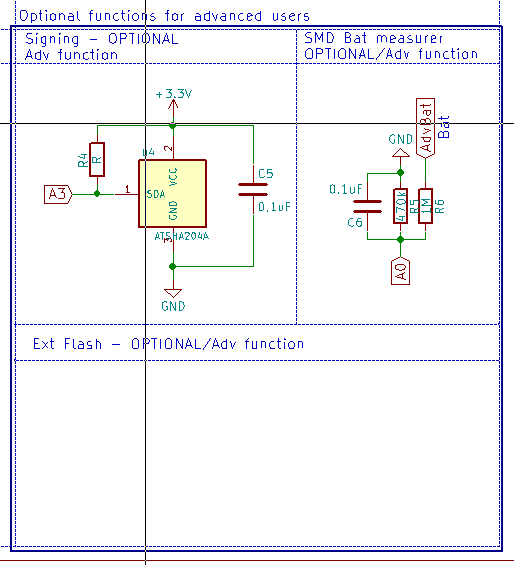
- Could you please post a JPG/PNG of the schematic in the design files section? (The schematic on the description page is a bit too small to read. Thanks!)
- You could save some space by changing the REG/BAT selection from jumpers to solder bridges, which can be squeezed into a lot more places on the PCB, especially on the back. However, the REG/BAT headers are useful both as a power switch and a great place to connect a multimeter/ammeter to measure the node's current draw, so I'd be a bit sad if you did this.
- There's enough space under the RFM69 (on the back of the PCB) to mount a CR16xx battery holder. Or if you relocate the adjacent caps, there would be space for a CR20xx battery (which are cheaper, higher capacity, and easier to find).
- If you were to make the whole right hand side of the board a prototyping area (i.e. clear of components), it would be exactly the right size to mount a 1xAAA battery holder.
- If you do bring Arduino IO pins out to the prototyping area(s), it would be really useful to put solder bridges in the traces (if space permits), or at least space the traces to make it easy to cut any that aren't wanted.
- A PCB trace antenna would be really cool!
I know that's quite a wishlist, and not all those ideas are compatible with each other, or the Nrf24l01+ version of the PCB, but I hope that provides some useful inspiration nonetheless.
Thanks again @sundberg84 :+1:
Blog: https://www.wes.id.au/
Nodes: Arduino Pro Mini ATMega328P 3.3V 8MHz, RFM69 433MHz, Canton Power CE024 0.8-3.3V regulator & single AA battery
Gateway & Controller: Raspberry Pi 3 + Home Assistant -
@sundberg84 said in Easy/Newbie PCB for MySensors:
the booster I designed it for, its pins were mounted the other way around which worked out great.
Perhaps an even better solution would be to provide two sets of holes for the booster, so that it can fit in the designated space regardless of which way round its pins are.
@sundberg84 said in Easy/Newbie PCB for MySensors:
Im thinking maybe I should move the resistors for battery measurment under the Arduino Pro Mini
Great idea! The only consideration is clearance if soldering the Arduino directly to the PCB, but resistors should be ok - the black plastic spacers on the header pins are 2.3mm high, and typical resistors are only 2.2mm in diameter.
You could even get away with putting caps under the Arduino, if you allow enough space for the them to be laid on their side if soldering the Arduino directly to the PCB. My 0.1uF electrolytics are 4.1mm diameter, so a directly soldered Arduino would have to sit about 2mm higher than normal. Or you could use tantalum or polymer capacitors, which should be less than 2.3mm high if laid on their side (but more expensive than electrolytics).
Some further thoughts I had overnight:
- Could you please post a JPG/PNG of the schematic in the design files section? (The schematic on the description page is a bit too small to read. Thanks!)
- You could save some space by changing the REG/BAT selection from jumpers to solder bridges, which can be squeezed into a lot more places on the PCB, especially on the back. However, the REG/BAT headers are useful both as a power switch and a great place to connect a multimeter/ammeter to measure the node's current draw, so I'd be a bit sad if you did this.
- There's enough space under the RFM69 (on the back of the PCB) to mount a CR16xx battery holder. Or if you relocate the adjacent caps, there would be space for a CR20xx battery (which are cheaper, higher capacity, and easier to find).
- If you were to make the whole right hand side of the board a prototyping area (i.e. clear of components), it would be exactly the right size to mount a 1xAAA battery holder.
- If you do bring Arduino IO pins out to the prototyping area(s), it would be really useful to put solder bridges in the traces (if space permits), or at least space the traces to make it easy to cut any that aren't wanted.
- A PCB trace antenna would be really cool!
I know that's quite a wishlist, and not all those ideas are compatible with each other, or the Nrf24l01+ version of the PCB, but I hope that provides some useful inspiration nonetheless.
Thanks again @sundberg84 :+1:
-
Im thinking maybe I should move the resistors for battery measurment under the Arduino Pro Mini
Great idea! The only consideration is clearance if soldering the Arduino directly to the PCB, but resistors should be ok - the black plastic spacers on the header pins are 2.3mm high, and typical resistors are only 2.2mm in diameter.
Maybe a better idea is to include a SMD voltage divider on the back for advanced users and not make the current voltage divider harder to use (by putting it under the pro mini)
- Could you please post a JPG/PNG of the schematic in the design files section? (The schematic on the description page is a bit too small to read. Thanks!)
I have posted for RFM Rev9. Nrf I will post as soon as Rev 10 is developed (Using Kicad now).
- You could save some space by changing the REG/BAT selection from jumpers to solder bridges, which can be squeezed into a lot more places on the PCB, especially on the back. However, the REG/BAT headers are useful both as a power switch and a great place to connect a multimeter/ammeter to measure the node's current draw, so I'd be a bit sad if you did this.
- I will not use any smaller / smd components on the top side. All main functions have to be 2.54mm/legs.
- There's enough space under the RFM69 (on the back of the PCB) to mount a CR16xx battery holder. Or if you relocate the adjacent caps, there would be space for a CR20xx battery (which are cheaper, higher capacity, and easier to find).
If you were to make the whole right hand side of the board a prototyping area (i.e. clear of components), it would be exactly the right size to mount a 1xAAA battery holder.
I will consider this... or maybe we can do some sort of pins for this on the prototyping area and make a tutorial.
If you do bring Arduino IO pins out to the prototyping area(s), it would be really useful to put solder bridges in the traces (if space permits), or at least space the traces to make it easy to cut any that aren't wanted.
I will consider this, but as mentioned I will not use smd bridges so space might be a problem.
A PCB trace antenna would be really cool!
- See @gohan answer.
-
@gohan said in Easy/Newbie PCB for MySensors:
@wes pcb antenna is going to be a challenge since rfm69 come with 3 possible frequencies
Of course (doh)
@sundberg84 said in Easy/Newbie PCB for MySensors:
I will not use any smaller / smd components on the top side. All main functions have to be 2.54mm/legs.
Sure thing; that's a good philosophy. To be clear, by solder bridges I meant two pads separated by a very small gap that can be bridged with a bit of solder, aka solderable jumpers:
(as opposed to SMD jumpers)
For your enjoyment, here 's a timelapse of a node I built today:
Blog: https://www.wes.id.au/
Nodes: Arduino Pro Mini ATMega328P 3.3V 8MHz, RFM69 433MHz, Canton Power CE024 0.8-3.3V regulator & single AA battery
Gateway & Controller: Raspberry Pi 3 + Home Assistant -
@gohan said in Easy/Newbie PCB for MySensors:
@wes pcb antenna is going to be a challenge since rfm69 come with 3 possible frequencies
Of course (doh)
@sundberg84 said in Easy/Newbie PCB for MySensors:
I will not use any smaller / smd components on the top side. All main functions have to be 2.54mm/legs.
Sure thing; that's a good philosophy. To be clear, by solder bridges I meant two pads separated by a very small gap that can be bridged with a bit of solder, aka solderable jumpers:
(as opposed to SMD jumpers)
For your enjoyment, here 's a timelapse of a node I built today:
@wes - so cool man! Thanks!
I have had in my mind for ages to do some sort of instruction / build video to be even more Newbie friendly. Is it ok if I link to this as a good build example on openhardware?About the solder-pads - I know about them - use them in other projects. Maybe I'm a bit over-concerned about this - I will have it in my mind as a solution.
Some initial schematics today.
Controller: Proxmox VM - Home Assistant
MySensors GW: Arduino Uno - W5100 Ethernet, Gw Shield Nrf24l01+ 2,4Ghz
MySensors GW: Arduino Uno - Gw Shield RFM69, 433mhz
RFLink GW - Arduino Mega + RFLink Shield, 433mhz -
@wes - so cool man! Thanks!
I have had in my mind for ages to do some sort of instruction / build video to be even more Newbie friendly. Is it ok if I link to this as a good build example on openhardware?About the solder-pads - I know about them - use them in other projects. Maybe I'm a bit over-concerned about this - I will have it in my mind as a solution.
Some initial schematics today.
@sundberg84 said in Easy/Newbie PCB for MySensors:
Is it ok if I link to this as a good build example on openhardware?
Of course. I can share the raw JPG images too if you want.
NB I used capacitor legs as header pins on the RFM69 because the proper header pins I ordered from eBay are still in the mail.
Blog: https://www.wes.id.au/
Nodes: Arduino Pro Mini ATMega328P 3.3V 8MHz, RFM69 433MHz, Canton Power CE024 0.8-3.3V regulator & single AA battery
Gateway & Controller: Raspberry Pi 3 + Home Assistant -
@sundberg84 said in Easy/Newbie PCB for MySensors:
Is it ok if I link to this as a good build example on openhardware?
Of course. I can share the raw JPG images too if you want.
NB I used capacitor legs as header pins on the RFM69 because the proper header pins I ordered from eBay are still in the mail.
@wes - you might have inspired me to try a instructions video myself :) I appreciate the jpg offer and thanks for letting me use it as a good example. Great example on how to build modular to be able to change or re-use hardware.
-
Im locking this thread (due to multiple threads). Please use this to discuss. https://forum.mysensors.org/topic/2740/easy-newbie-pcb-for-mysensors


