In wall light switch node - Custom PCB


  • Hardware Contributor

    Hello.

    My first contribution to MySensors is going to be a Light Switch node that meets a few lines of criteria. To my knowledge, this hasn't been developed yet and feel that there would be a fair few people that would benefit from a very simple switch node that actually fits in a location where an existing switch does, that way there is no signs of home automation on the switch front. Yes we have scene controllers that can be mounted onto the wall, but this starts to become bulky and obvious that there is some sort of technology there controlling something, what about if you simply just want to switch a light on with natural instincts without having to look at what you're doing? This is where I personally think this Product would prove itself worthwhile. There are currently two other projects like this going on here at the MySensors forum:
    @sundberg84's In Wall PCB - This is a node using two PCB's stacked together that will sit inside of Swedish style wall appliance box and have its own power fed to it.
    @martinhjelmare's: Box for In Wall PCB - This is a box that simply sits inside of the socket to contain all the open high voltages of electricity if being reduced down from 240v on the PCB itself.

    If there is any electricians roaming around here, please, advise me of any serious, specific implications, rules and regulations that this would need to meet that i haven't stated so. I will be getting some mock schematic and PCB designs sorted out for you guys to look at for a starting point. I will make it very obvious now that I'm not a profession electronics guy, nor am i someone that has experience in designing PCB's, electronic designs or anything. This is a huge learning curve for me, but as a community i do believe we can put together some awesome products, alongside of @sundberg84 and @martinhjelmare's proposed outcomes.

    Product Criteria:

    1. Fits inside of a slimline (25mm depth) UK Wall metal AND plastic back box/dry lining box.
    2. Able to be powered via Battery and/or mains electricity, either 240v straight from the power circuit or have it transformed down to the 5v in a central location/outside of the socket box then fed into the box for application.
    3. Allowing you to keep existing wires in the box, but terminated. This would allow us backward capabilities of reverting our alterations in case of selling the property.
    4. Form factor/Footprint must be a small as possible to remove any possible issues on the space allocated.

    The Product itself:
    The product itself will be based around an Arduino Mini Pro powered via either a cell coin battery, AA batteries or a mains electric feed reduced down to the required voltage, I'm thinking 5v step down outside of the box (in a central location, maybe even in the electric room (where your main breaker is located) then stepped down from 5v to 3.3v on the board itself. The whole system will be created and located onto a custom PCB that i propose to be all SMD, to allow for a smaller form factor for the already challenging installation size. This product will start out to be a simple ON/OFF switch, a dimming version will be the first upgrade offered to the product. The product will include a nRF24L01 radio transceiver to deal with its networking, so that is going to need some revision for the metal back box version to allow the transceiver to work with the metal, if it has issues that is.

    Currently, I have a breadboard setup with an Arduino Nano, a light switch faceplate doing the switching and an nRF24L01 doing the transmitting back to my MQTT gateway. So currently outside of the Arduino, all that is needed is terminals for the switch itself and a resistor for the switch. Then we will need the power solution, so a coin cell holder, resistors, caps whatever is needed to feed a stable 3.3v to the micro controller. The mains connection, this is going to need screw terminals, and again caps, resistors and whatever else is needed to reduce down the power (I'm still thinking to bring the mains in at 5v, so step them down outside of the application). If anyone feels like pointing me in the right direction in terms of whats needed to bring mains power down, feel free. I will continue to research the correct ways to do such a thing in the meantime.

    Environment Design work:
    I have made a pretty accurate design in google sketchup as a starting environment for the first installation of this product detailing sizes that we have to work with to enable us to fit this inside of the existing wall back box.

    Light Switch.png

    The Environment for the Product:
    For example, the below images show a light switch placement that i currently have, hopefully this will give some indication the room that we have to work with here to allow the existing cables to be terminated and left where they are for future needs. A normal back box or dry lining box installed now would be 35mm to sometimes even 50mm boxes, however we must allow for such situations that arise where the plasterers (Like myself) have had no choice but to install a 25mm box.

    DISCLAIMER: I did not install the current switch, which as you can see is a pretty poor installation to say the least. I will be using an electrician to do any mains electrical work, and therefor I'm not going to allow anything below the national standard to be installed into my property.
    IMG_6882.JPG

    DISCLAIMER: I do not advise you in any way to make/install this product into a property and therefore I take no responsibility for any issues, problems you have or even health implications that you endure while completing the installation or even using the product after installing.

    UPDATES

    24th December 2015 - Version 1.1 Revision 1 boards have been ordered and currently being produced with ITead.cc.
    24th December 2015 - Parts have been ordered for the production of 1 evaluation node.
    14th January 2016 - Version 1.1 Revision 1 board has arrived, populated with components.
    23rd January 2016 - Version 1.1 Revision 2 boards have been ordered and currently being produced with ITead.cc.
    13th February 2016 - Version 1.1 Revision 2 boards have been received and populated.
    19th February 2016 - Version 1.1 Revision 2 boards are currently going through their first 24-Hour long testing period.
    21st February 2016 - Version 1.1 Revision 2 boards are undergoing troubleshooting work.
    5th March 2016 - Version 1.1 Revision 2 boards are completed and power usage tests are currently taking place.
    19th March 2016 - Version 1.1 Revision 2 has been uploaded to https://www.openhardware.io/view/48/Homini-In-Wall-Battery-Powered-Light-Switch-Module

    FILES
    Current Eagle Files - Homini_Light_Switch_Node_Version_1.1_Revision_2.zip
    Schematic PDF - 1_1457169973710_HominiSwitchNode1.0Rev2_Sch.pdf
    Board PDF - 0_1457169973709_HominiSwitchNode1.0Rev2_Brd.pdf
    Gerber Files - 0_1457460927449_Rev2 Gerbers.zip
    BOM - 0_1457593789223_HominiSwitchNode1.0Rev2BOM.csv


  • Hardware Contributor

    Hi.

    wow, it's great, lot of inwall projects...I agree with you for smd, I think it's best suited for slimmer as we have not much place inwall..the biggest problem is the ac stepdown, it takes lots of place. if we want something as small as "fibaro" it needs a custom ac stepdown. it's a little more tricky to make well but doable, then it is not galvanically isolated, not the the biggest problem if it is well integrated I think.

    Then there is multiple connections existing inwall to connect the switch. 3wire or like at my home for instance, I have only 2 wire connected on my switch one from mains, the other one go to the lamp. And this case is much more tricky to do...it needs a very smart power (lot of work on this) to power the device. the easy way for this one is coincell or battery.

    If it can help, and you do it before me 😉 because I have some projects in work but it shoud not take too much time to design..
    In my case, for the moment, I plan to have:

    for powering options, I am not very sure to be able to have all these options on one board but I will try to see 😉
    I wan to keep the "motherboard" on bottom, and of course, the sensors shield on top, so when opening the switch, we can't touch ac parts...lot of others ideas but I let you make your own. I don't want to interfere in your ideas 🙂


  • Hardware Contributor

    Great to see all this projects come to life! I hope we all can gather around this and create a great, small and SAFE in wall product.


  • Hardware Contributor

    @scalz - FIrstly i would love to have some sort of development input or even help you on your project once my idea has got going. Just one question, the only rs485 i know is that of the serial connection for computers, could you explain what your mean by powering via rs485 please? For Version one of my product I will be keeping it nice and simple and keep it to just the one board with screw terminals for the switch buttons. Hopefully Version 2 will bring upgrades such as a secondary (sensor) board where we will then be able to connect different sensors onto the daughter board without touching the AC/DC like you have in mind. I would like to keep everything in this thread very simple and one at a time to enable us all to have a clear working space to develop the product that is in mind. Then once we have achieved that, then we can then agree what upgrades would be worthwhile and then develop Version 2. I will be documenting everything that goes on with this product just to make everything flow as smooth as possible with reference points at every stage of the build. I'm hoping that this will help prevent any issues that would require us to rollback to a previous state/build. I came across your 'MyTinyCamel' build the other day, i love what you have done!

    @sundberg84 - That is exactly what I would love to happen, and I'm pretty sure the likes of @hek will be loving that fact he has developed such a tight and strong community that is coming together to develop what the admins would call their 'baby'. I look forward to every upgrade we make! Bring on the issues and lets develop as a community!


  • Hardware Contributor

    @samuel235: thx 🙂 sorry, like I said I don't want to interfere in your projects. I was just saying some ideas if it can help.
    for rs485, it is just I will use one pair for power and one pair for data. I know it's possible to power and data on same line but this is not the way I will use I think.

    so, good luck with your project 😉


  • Hardware Contributor

    @scalz Ahh so it is the serial cable you speak of! I would honestly really appreciate your input on this topic. I don't want you to leave from the topic at all. Please, share your inputs and suggestions whenever you feel the need, just want to keep everything organised here, so it doesn't end up with a caotic mess. I luck forward to your suggestions on various issues and upgrades along the path!


  • Hardware Contributor

    I have attached the Board and Schematic mock-ups. Would it be possible to hear your opinions on what needs to be changed, if anything that is. All being well the RF Module fits where i intend it too, sitting just above the chip itself.

    Does that capacitor look okay being grounded to the ground line rather than directly onto the ground pin of the RF module (To stabilize the vcc and ground of the RF module).

    A quick little list to show what is what on the board:
    AVR CONNECT - Connection for AVR Programmer to bootload.
    SW1 - Screw terminals for Switch 1.
    SW2 - Screw terminals for Switch 2.
    SW3 - Screw terminals for Switch 3.
    ATMEGA328P-AU - The obvious, ATMEGA328P-AU.
    NRF24L1 - NRF24l01+, will use header pins and solder so its sitting just abover the ATMEGA.
    C2 - 4.7uF Capacitor to bridge the VCC and GND on the radio.
    BAT1 - Cell coin holder (CR2450)

    I don't need any mounting holes at the moment so that isn't an issue. I plan on elevating it off of the metal back box to stop any chance of shorting too.

    Would you say that i need to be wiring the terminals for the switch using VCC and a resistor or would a input pin to ground be okay? I've seen so many people people do it both ways in the forums and on the general internet, what is the preferred method?

    I'm more than happy with receiving any sort of criticism on this board, as this is my first attempt of a custom PCB and my first attempt of using Eagle software.

    Sch1.jpg Brd1.jpg


  • Hardware Contributor

    Why not use a 4-pol screw terminal instead? One common and then one input for each switch. Also, consider if the corners could be 45 degrees instead of 90. That would make it fit more easly in a round back box. Aren't you missing a pull-up for reset and a few decoupling caps for the ATMega?


  • Hardware Contributor

    Indeed, decoupling cap (100nF) is needed or the powerline (VCC-GND) would be unstable when transmissions occur. This effect could block or reset the atmega.
    With this setup, you will not be able to program sketches when the NRF is connected. If you add an FTDI header, you can program via serial port and monitor the processor while the NRF is connected. Will help in debugging code.


  • Hardware Contributor

    @mardah @GertSanders - Sorry guys, for some reason i just assumed that the decoupling caps were only needed for if i was using an external crystal, for increased power needed for 16MHz. I'll get that on.

    I'm going to have a look at that header you speak about when i get home tonight, i was planning on programming the board then soldering the RF module on. Now you point this out that would be a very silly amature mistake to do. Thank you for making that obvious.

    I'm also planning on refining the layout of the board and the shape. So i will take the corners off to adapt it to a round box.


  • Hardware Contributor

    You might want to have both the 1x6 pin FTDI-serial-"arduino" port and the 2x3 pin AVR ISP port. Note that pin# are standardized.


  • Hardware Contributor

    @m26872 Could i ask why i would need both? They essentially do the same thing, right? Except FTDI uses the DFU bootloader and then the SPI connection overrides the DFU bootloader, am i correct in thinking this or do i have my lines mixed up? If so then i was planning on using the 6 pins i have on the edge of the board, connect them via jumper cables to the 6pin SPI connecter that would come with the USBasp programmer i plan to purchase. The reason i plan to go down this route is simply to save room in the socket, limited height room.

    @GertSanders - Is the 6 pins that i have added to the board not a FTDI header? What makes it not, the pin layout or the pins used on the mega chip? I thought that if i added 6 pins, wired them to the chip using the pins i have (gnd, vcc, ce, csn, irq, miso, mosi and sck) that made it a FTDI, I'm guessing I'm incorrect?

    @mardah - Free space depending, i'm looking into doing this now, so do you feel that my switching method is sufficient enough without using vcc and a resistor to each switch and then to the input pin? You're happy with the Input pin -> switch -> GND method? EDIT: The only 4 Pol i can find that would be big enough to accept 3 cables into the common is working out at a stupid price in comparison to the rest of the board. At the moment, i will be using the 3 terminal setup i have currently sketched.

    I planned on using this as the USBasp programmer, however if i can use just an FTDI connection to do both (program the MYSBootloader and to upload sketches) that would be better for saving space on the board.

    The FTDI programmer: Link
    Can you use this to program the MYSBootloader as well as upload a sketch or is this simply to upload a sketch to the mega?

    The decoupling caps, as a rule of thumb, its 100nF cap per supply pin, correct? I will supply all 3 VCC pins with the power, so i should connect a 100nF cap to each of the pins. Does this sound over kill or okay?


  • Hardware Contributor

    @mardah If i wire a 4-Pol screw terminal as follows:

    1 - GND
    2 - INPUT1
    3 - INPUT2
    4 - INPUT3

    Then i wire GND into Switch1's COM connector, then L1 goes to screw terminal pin 2 (INPUT1). Then i take the com from the back of Switch1 into the COM connector of Switch2, then wire Switch2's L1 connector to screw terminal pin 3 (INPUT2) and the same for switch 3. Do you feel this would work as intended?


  • Hardware Contributor

    hi.

    just a little thing, it is "better" to have nothing under radio antenna (no gnd plane..) for range and operation. it could help as it will be inwall 😉


  • Hardware Contributor

    @scalz Thank you for that heads up, i will get that down onto my board documents to change too. Thank you!


  • Hardware Contributor

    @samuel235 I can't tell you what you need, I'm just saying that if you provide an AVR-ISP port looking like FTDI-port, everyone except yourself will be confused or even risk to destroy the AVR by mistake.
    Let's look at the Sensbender diagram as a reference. The FTDI-port is JP2 and the AVR-ISP is JP3. Most people would prefer to program bootloader once and then use the FTDI to upload and debug new programs.
    If I couldn't fit an AVR ISP port, I would try to make to make the nRF SPI-pin + Reset, accessible. Maybe even better is to make (if you don't already have?) a special board for 328p-AU (TQFP-package) bootloader programming, then solder it in place with bootloader already on it.
    Please also note that the JP2 FTDI-port needs R3 and C5 to work.


  • Hardware Contributor

    @m26872 Firstly, thank you for referencing the sensebender and its pinout. I can now have a look at this and use it to better improve the pinout and layout of my board. So, i will try to get both headers onto my board to allow better programming capabilities. If i use the same pinout as the sensebender does for the AVR ISP and the FTDI-port, would i then be able to burn the bootloader and upload sketches while the RF module is soldered. If not, do you think i could use some jumper headers to effectively remove the RF module from the board while I upload the sketch and then put the jumpers back on to close the circuit back up?


  • Hardware Contributor

    @samuel235 I can't recall that I've actually used the ISP with the nRF, but the whole point of ISP is that it should work.


  • Hardware Contributor

    @m26872 Okay, so its probably best to just burn the bootloader, then solder the nRF inplace and then upload the sketches using the FTDI port just in case i solder on the nRF then turns out i can't burn the bootloader?

    I believe i can leave the AREF pin unconnected. Is this true?

    Do you have any other input other than the following changes i'm scheduling to make on the board tomorrow:

    • Remove GND plane around the area of nRF module to reduce chance of interference.
    • Remove current screw terminals and replace with 1 4-Position with GND as common and other 3 going to input pins.
    • Connect all GND pins.
    • Connect all VCC pins.
    • Add decoupling Caps in the layout that Sensebender uses, 1 on each VCC, so 3 in total.
    • Add Pullup to reset pin.
    • Remove current 'FTDI' connector and add correct FTDI layout connector along with a SPI header connection for bootloading, use Sensebender for reference of the pinout for these two connectors.

    While looking through the Sensebender schematic and images, i have noticed there is Q1 (What i think is a transistor, correct me if i'm incorrect), may i ask if you know what this is for, as it is not actually on the final board images.

    Sorry if i have made any more school boy errors.
    Sam.


  • Hardware Contributor

    @samuel235
    Arduino Pro Mini should be your no1 reference. Schematics and Eagle files povided. There your can see the normal layout of Q1 e.g. It's the crystal/oscillator (with 22pF caps if you choose xtal) I don't know why Sensebender looks like it does.

    I haven't studied your design closely or know your intentions, but I don't know of any proven coin cell nRF designs, but I suppose you'll have it sleeping a lot.

    Sometimes it's good to breadboard prototypes if there're any hesistance.


  • Hardware Contributor

    for coincell, maybe you could add a capacitor near the coincell to absorb spike of power consumption..so the coincell would not discharge too fast with sudden spike 😉
    maybe 47u or 100u if you add few sensors in future...100u not very cheap..maybe through hole, there are some not too big.


  • Hardware Contributor

    @m26872 I have been looking at a nano i have on my desk while building these designs, and i didn't notice anything with Q1 hense why i asked about it on sensebender. However it is not of any interest to this project (to my knowledge), i just wanted to learn the use of a tran in this case.

    I will be sleeping the module quite a bit yeah, literally asleep all the time until someone presses the switch.

    @scalz I'll throw a 47u in there, this node shouldn't be used for any other sensor at any time to be honest, hence why i'm designing it from scratch to go into the socket.


  • Hardware Contributor

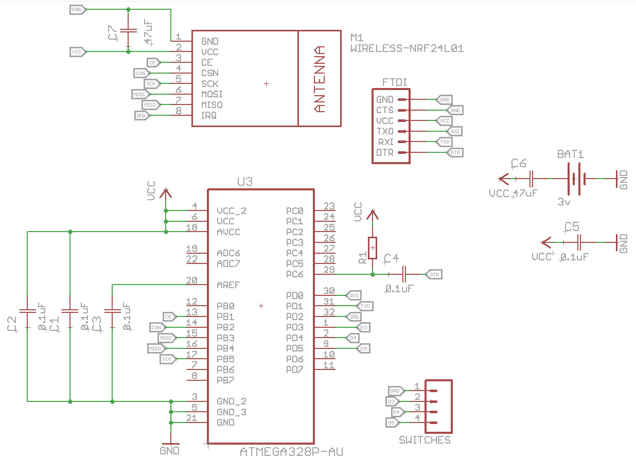
    Tonight i have finished updating my schematic to reflect some of your helpful inputs. Please, again, throw any comments you have regarding my layouts my way so i can further improve the board if needed. Upgrades i have done are:

    • Added Capacitors for the VCC lines.
    • Added proper pinout/layout for the FTDI header.
    • Added a Capacitor on the battery to stop any spikes of current draw.
    • Changed the double position screw terminals for a 4 position one.
    • Added a pull-up resistor and capacitor on reset pin for the FTDI uploads to be able to reset upon new sketch upload.

    Currently i still do not have a SPI header included. Would i be able to survive without one, could i do the sketch upload through the FTDI header at all?
    Once i finalize the overall board layout i will know what size i'm working with and IF i can fit a SPI header in, i will install one onto the board. However, because of the limiting space i may struggle on this.
    Sch2.jpg


  • Hardware Contributor

    Looks proper. I think those two 47uF caps don't necessarily have to be two and can be placed anywhere between vcc and gnd, provided short low resistance traces etc.


  • Hardware Contributor

    @m26872 - Do you feel it would be perfectly fine to remove the Capacitor thats directly on the battery then?


  • Hardware Contributor

    Either you breadboard your design first or make it a flexible pcb design.

    Add footprint and make room for bigger or more caps just in case they'll be needed. The physical place shouldn't matter.

    Edit: Since someone will object to that last sentence if I don't clarify it .... Physical place of that 47uF near nRF could matter, but if so - it should be fixed with some small low ESR cap near it instead.


  • Hardware Contributor

    @m26872 So just to clarify, do i understand correctly that you're suggesting to remove the battery capacitor, keep the nRF cap in there and just allow a few VCC -> Capacitor -> GND dotted around the board to allow me to add more caps if needed?


  • Hardware Contributor

    Ok. Leave the 47u near nRF as it is. Make the footprint for the other 47u one, but make it fit even a 100uF if there's room for it. Only populate if needed. And yes open footprints for 0.1uF caps dotted around is not bad either.


  • Hardware Contributor

    Awesome! I have that all sketched out now. For the passive components i have gone with a size of 0603 SMD. Would this be the cheapest? Or would 0805 be for its popularity? Cost of pense isn't really an issue for me however i would like to have a really cheap source price for this board as another positive point for it, but again its not vital.


  • Hardware Contributor

    @samuel235: cool.

    • I think you need to learn some basic electronics basics guide, it could help you in future to understand because if you want to draw schem, it would be useful, positive feedback 😉
      I started to learn elec and uc stuff some years ago(10+), so when I say I am not electronician, it is a small lie 🙂 I am not graduated in this field 😉 but my dad, elec engineer, teached me a lot. I am lucky. Now you can have lot infos at sparkfun, adafruit, arduino ....and you are choosing the fun/interesting way, learning learning and learning.
    • like @m26872 said, it is better, and I like it too when I can, to have footprints.
    • for the batt cap, I told you this because of the cr2032 comment..it can prevent the coin cell to discharge too fast. coin cell don't like spikes, this is one of the reason for people choosing alkaline. but you can do lot of stuff with coin cell too. the cap is optional of course.
    • If you can have avrspi, better, but if no space. like you said upload bootloader, and then...if you have to reupload it later, just unsolder nrf, not big thing.
    • for 0805 or 0603, this is not a question about component cost here...it is much more a question of your soldering skills and available space of course.
      I have no problem with 0603, I handsolder some vqfn sensors (very hard stuff...), but what I would advice for noob, a step by step curve. Try 0805 first, then move harder stuff. You will see that you must be careful when soldering atmel tqfp. If all ok, then...pcb are cheap now 😉 I hope you have good iron solder, thin wire....

  • Hardware Contributor

    ... and flux.


  • Hardware Contributor

    @scalz - This is partially why i'm choosing to do all of this myself, I'm learning electronics while i go. Honestly, its why i have created this topic/thread so i can learn and other can tune in to learn a thing or two as well. I have that Cap wired into the battery if i need it, i will more than likely just put it in anyway to be on the safe side. I think I'm going straight into 0603 SMD tbh, I have a pretty steady hand and have some decent soldering experience. I may need to get myself a expensive/quality soldering iron, i have a cheap(ish) temperature regulated one at the moment. I'm getting some thin solder on order with the parts when i finally order it all.


  • Hardware Contributor

    cool. so, for soldering, from my own experience, but I will start to use reflow oven, what I can advise you is:


  • Hardware Contributor

    @scalz Pretty cool list of things there! I'm going to use the soldering iron i have at the moment and see how that stands up to the task. I will be ordering a magnifier, some thin solder, a few tweezers, desolder wick and some alcohol too. I have been doing some pretty basic soldering jobs where i didn't need to pay close attention as much as this in terms of little things like cleaning up the board etc etc. I have soldered and replaced laptop motherboard power connectors and such, completed the PCB Board kits for little projects but nothing as serious as this before. So now is the time my soldering skills are going to be put to the test, and i honestly can't wait! I'm working on my board layout as we speak and i will get this uploaded soon as i am done for a update to the project.


  • Hardware Contributor

    I'm very tempted to have some jumper headers or even a dip switch on the board to allow for sketch uploads with the nRF intact. I'm hoping to get some sizings done tomorrow and if i have the room i may have the RF module on a header/socket so i can remove it while uploading a swetch. If not i will have to go with the idea of jumpers or try to rearrange the board to allow a SPI header. I shall see what i can do, upload to this build log and see what you guys think. Again, with shared input we could possibly create a much better suited board then.

    Whats your opinions to the jumper pins across the SPI connection on the nRF module to effectivly disconnect the RF while we upload the sketch upgrades?


  • Hardware Contributor

    C6 should be in parallel to the battery. In the schematic you show, the C6 would disconnect the battery from Vcc (from DC point of view). If you have Vcc - C6 - battery- GND, then no DC current will flow from Vcc to GND. Is should be:
    Vcc -+- battery -+- GND
    Vcc -+- C6 -+- GND


  • Hardware Contributor

    @GertSanders I should remove C6 from the battery to make VCC - BATT - GND. Then put it like i have done with C5, as VCC - C6 - GND. Have i understood you correctly?


  • Hardware Contributor

    C6 // Batt
    one side of C6 to VCC/Vbat
    other side of C6 to GND


  • Hardware Contributor

    @scalz said:

    C6 // Batt
    one side of C6 to VCC/Vbat
    other side of C6 to GND

    Thank you for confirming that Scalz, i'll get that updated tonight 🙂


  • Hardware Contributor

    @samuel235 you understand correctly 🙂


  • Hardware Contributor

    I have added a ISP header, 100uF cap through-hole footpads, i may remove one of the two 47uF caps, don't feel i will need two 47's and a 100, i'll keep the pads there for it but wont add it just yet.

    I'm now just playing around with the layout of the board, at the moment i have it down to around 1.2inches by 2.8inches. It would be alot slimmer if i didn't have a 24mm batt onboard. However i don't want to be changing the battery every month, so i opted for the bigger size of the batteries. Once i have the layout, i'll do some drawings and models of this to enable me to see if it will fit my application.

    The RF module is adding to the overall size because i'm trying not to have it mounted over the top of anything as adviced to reduce chance of interference.

    I will get some images up tomorrow for an update to this build log.


  • Hardware Contributor

    Current situation:

    I'm really struggling with the composition of the board to enable me to fit this into the slim socket back box, I'm now giving it a thought to mount the radio over the board. However this is still coming VERY tight to fitting, mainly because of the size of the switch i have chosen, it extrudes quite a way back into the box (as shown in the Sketchup model in the original post, at the top of this page). I only have 11mm behind the middle of the box, the battery mounted plus the board and plus 5mm mounted capacitor (applicable in the first image shown below where the radio is overhanging the edge of the board) would equal around 12mm, so even at an angle i don't think this board would fit in there.
    brd.jpg
    So that is why i looked at the idea of moving the cap out of the way to the other side of the board, putting the radio down onto the bottom of the board but keeping its orientation. I think this may reduce the thickness of the overall package slightly, will still be very tight (within 1mm i think), but a possibility it would fit (maybe). Shown in the design layout below. I think if i could remove the black plastic standoffs on the header for the radio and mount it practically touching the board itself then i may have a chance to get it in.
    brd2.jpg

    First of all, do you think that there would be any issues with the layout i have placed in the second design? As far as I can see i have done the main things like keeping the caps next to what they are intending to protect, kept under the radio board clean, have 1 x 100uF cap for spikes on radio and 2 47uF cap's for additional large spikes, 0.1uF caps are dotted around the bottom to reduce small spikes, managed to get a SPI and FTDI header included with all the resistors and caps needed.

    The last few days I'm sitting at the stage of just rearranging the design to fit into my environment, I may have to change the backbox if needed but i would prefer to manufacture the board to fit into the smaller space if possible. but if physical limitations are there that is impossible to work around it would leave this as the only resort.


  • Hardware Contributor

    As the night draws to a close, it would appear i have found the physical sizing issue solution! Now, just for the routing to be done. Another stage, another day! As this project gets closer to a completed board, the more I get excited about the manufacturing of my first ever useful custom made PCB. After all, this is what a community built project is all about, experienced users helping armatures become experienced to help armatures, isn't it? I'd like to just take this post to thank everyone that assisted me so far with this project!

    The remaining steps:

    • Add MySensors' logo/branding to the board.
    • Complete the routing of the board.

    brd3.jpg


  • Hardware Contributor

    Good morning guys, just to keep the topic updated with the latest info on this project;

    I'm still currently designing the board, trying to move parts around and route the traces. Because of everything being so cramped I'm having a real hard time getting this done. I'm having a couple of issues here where i can't get traces from certain points (top left corner) out and around the through-hole components so i will need to be moving some things around again, but I'm constantly pushed on a cramped space to physically get this into the light switch. One of the biggest issues i have is the terminal block, I may remove this and just end up soldering the switch cable directly to the board. The other issue i have is a software issue with eagle and ITead manufacturer, I'm creating routes with >8mil thickness (the website says that 6mil is minimum), then using their checking DRC file, and its throwing back errors relating to the trace width, however if i create the traces in 10mil its fine. However, there is just no way at all i can get away with 10mil 😞

    Today's agenda:

    • Remove screw terminals.

    • Relocate the micro controller under the nRF board, not under the antenna section though.

    • Relocate some of the components around the top of the board to allow traces through.

    If i could get some feedback from you guys on the following, it would be appreciated.

    • Do you think I might be able to route/trace on the bottom layer under the antenna section (Antenna will be sitting about 2-5mm above the top layer) without receiving interference.

    • What do you think about my DRC Check errors? ITead say >6mil but i get errors on 8.5/9mil.


  • Hardware Contributor

    hi @samuel235 Check the rules spacing between traces. Trace width needs to be minimum 6 mil, but space between traces also has a minimum, maybe this is set higher ? I have used this DRU file and so far always had good boards from manufacturers.
    Gert_Sanders.dru
    Maybe this helps your tracing issue.


  • Hardware Contributor

    Good evening @GertSanders - There is nothing else on the board, I'm literally testing this on a clean board file, nothing on it at all. Just 1 wire. So there for there is essencially nothing to make a spacing issue around the wire. I have just tried to do it on any other layer than top or bottom and it doesn't create an error.... Is there any area of the DRC checks that only apply to the width of the top/bottom traces?


  • Hardware Contributor

    hi @samuel235 Beats me, if there is only 1 wire then maybe you have a conflict between the net class and the DRU. But I do not know what would be the issue without trying the same DRC check on your board file.


  • Hardware Contributor

    @GertSanders - I have just tried your DRU file, its doing it for that too.... Your minimum width and spacing is set to 6mil, i've ran my routes in 8 and 12.

    EDIT: Turns out you were correct in advising the net class conflict, i went into the net class editor and it is set to 12mil so i changed this to 6 to double check, and it works perfectly. Can i leave this at 6 without any issues or is it there for a specific reason? I'm going to have a little research on these net classes because i honestly don't understand their purpose when they are set to a value above that of a custom DRC check.


  • Hardware Contributor

    hi @samuel235 The netclasses allow you to differentiate trace widths and spacing automatically when using the autorouter. If you do nothing, then all traces are routed by the autorouter according to the DRU. In the Netclasses you can overrule the default trace width and spacing to be respected by the autorouter.

    When you check a trace (checking it's attributes) you can see to which net class it belongs. It is mentioned at the bottom.

    Why different netclasses ? For example if you use power lines on your board, you could want them to be wider and have more clearance from other wires. To be able to check that the extra clearance is respected, you can define extra clearance in a net class called "power" and then make those wirelines for the power net member of the net class "power". If you use the autorouter, and you defined a width of 20mil for the power net, then the autorouter will make those traces 20mil wide. If you defined a clearance of 15mil for the power net, then all traces different from that power net need to be routed at least 15mil away from the power trace (e.g. Vcc signal or GND signal). If you trace by hand, then sometimes one could be tracing a signal line too close to a power line, and when doing a design rule check, the net class limitations are taken into account.


  • Hardware Contributor

    @GertSanders I think I explained incorrectly, i understand that the net classes are for the autorouter and how you can tell the auto route to do different classes for different instances. But what i don't understand is why if i have manually routed everything, why is the drc checker using the values on net classes, is it just as simple as changing the net classes to the board houses specific requirements?

    Also, would there be a way to create different profiles for the net classes for each board house, just like how you can create different drc files for different needs?


  • Hardware Contributor

    @samuel235 If a DRU file species that two signals need to be a minimum of 6mil apart and the net class requires that different signals need to be 8mil apart, then the larger spacing is what counts. If your default net class has a larger spacing minimum then the DRC of a board house, then you need to follow the net class definition when doing manual routing. Autorouting takes into account the most stringent requirement automatically.

    You can have several DRU files, but I do not know if you can link them to specific netclasses.


  • Hardware Contributor

    @GertSanders Ahh okay, that makes complete sense now. So the default is set to Width: 10mil, Drill: 20mil, Clearance: 10mil. ITead specify Width: 8mil, Drill: 0.3mm, Clearance: 8mil, I took these figures from here.

    So I am safe to change my net classes to those of the board house to run the checks and then revert them back once i generate my gerber files? Or have i miss understood?


  • Hardware Contributor

    @samuel235 You can change the defaults to the values of the boardhouse and leave it at that. When generating the GERBER files, the DRU or net class values are no longer important. You only need the values when checking against design rules.


  • Hardware Contributor

    @GertSanders said:

    @samuel235 You can change the defaults to the values of the boardhouse and leave it at that. When generating the GERBER files, the DRU or net class values are no longer important. You only need the values when checking against design rules.

    Awesome! I shall get it checked and posted here in a minute and hopefully I'll get it ordered tonight 🙂


  • Hardware Contributor

    And the final designs are shown below. As you can see the one on the left is without the ground planes and the one on the right is with them. If anything is jumping out in terms of errors or discrepancies, please don't hold back, let me know 😉

    Brd4.jpg


  • Hardware Contributor

    UPDATE!

    Just a little update to keep you all posted; I have sent my Gerber files off, they have been confirmed to be of the correct format and my boards are now being produced. I ordered the parts last night, enough for backups/errors, soon as everything arrives i will get this made up and give you another update on the situation of the board. The only thing i wasn't comfortable with was the price of the screw terminal and the fact i used a through hole capacitor for the 100uF (C7). The next revision of the board i will be using a surface mount 100uF capacitor for this, now i managed to find it. The terminal for the switches, I'm looking at maybe having a crimped push connector on the switch that just slots onto some sort of header pin on the board instead of a screw terminal.

    Either way, Homini Light Switch Node Version 1.1 Revision 1 is on its way!


  • Hardware Contributor

    I have just received confirmation that the board house has released the PCB's. Lets see how long these take to get here! Itching to get this module on the move again. I will be back soon as they get here, don't go anywhere!


  • Hardware Contributor

    UPDATE!

    I have just received all components for the boards, we're just waiting on the boards themselves to arrive from ITead Studios.

    Time to get this project moving!


  • Hardware Contributor

    While waiting for my boards to arrive i decided to create a housing for my gateway including flashing status LEDs. Its in no means a finished product, but i feel its enough to house the gateway components while i'm building my network to save any incidents destroying the parts. Within the next few days i will get a guide up with images and maybe a video of the LEDs and their function up on a hardware guide topic. image.jpg


  • Hardware Contributor

    So then, we have another update!

    UPDATE!

    The boards ave arrived safe and sound, i have populated one of them with everything apart from the nRF module. So, its time to get the bootloader burnt. This is the daunting task for me, i have no idea what i am doing here, so if you guys feel like you could give me some helpful pointers in the right direction I would really appreciate all the help you can offer.IMG_7098.JPG IMG_7099.JPG


  • Hardware Contributor

    Hi! Depending on which bootloader you want, but why not go with the MySensors with OTA updates by tekka?
    http://forum.mysensors.org/topic/838/windows-gui-controller-for-mysensors/75

    If you want the original arduino bootloader: https://www.arduino.cc/en/Hacking/Bootloader?from=Tutorial.Bootloader


  • Hardware Contributor

    @sundberg84 - I was reading that exact post from tekka as you posted this. However, i'm probing around on my board and found for some reason my 3v line is 0.24v. So I have to do some investigation work on that this morning. Hoping the bootloader will be a piece of cake once the hardware is working as should be.


  • Hardware Contributor

    @sundberg84 So i have my hardware issue corrected now. Am i reading Tekka's instructions correctly, this new board is to be connected through serial to my gateway and then programmed essentially by the gateway through MYSController which is connected to my gateway via ethernet? Does that sound correct?


  • Hardware Contributor

    No, i would recommend you have a look at some youtube tutorials. Im not familiar with programming through the ISP headers which i think you should do. I use a seperate arudino uno as ISP programmer.


  • Hardware Contributor

    @samuel235: cool. happy for you.

    first you need to burn the bootlader in your atmel 328p. When it comes as ic-only, factory setting is 1mhz internal rc. and there is no bootloader yet. So you can't use ftdi at this moment, nor ota. So you need to burn the bootloader with avrspi. Like @sundberg84 said you can use the "arduino uno as isp programmer" method if you have an uno..On my side, I don't use this method, I prefer to use an usbasp. But both method works well.
    When burning bootloader, you will need to set fuses too, corrsponding to the bootloader.

    Sorry, I have not much time to make an howto, just point you in some direction..i hope it helps a little bit.

    Edit: you can find some howto here http://www.gammon.com.au/breadboard


  • Hardware Contributor

    @scalz I'm using a USBasp programmer, however i think i may have an issue with my reset pin. I have continuity on every other ISP header pin and the associated pin on the ATMega but not the reset pin. Is this normal, should i be seeing continuity between ISP RESET and pin 29 on the ATMega?


  • Hardware Contributor

    I think you should have continuity between avrspi connector RST pin and your atmega RST pin...don't see why not. Have you checked your routing? I think so...Maybe a bad solder on this pin???


  • Hardware Contributor

    @scalz I may have found the problem, i have just completed a x25 magnification inspection on the boards and every board has atleast one filled VIA. I'm going to get a makeshift jumper in place on this board and test for continuity again.

    I get continuity from the pin to the one side of the capacitor but nothing from the MEGA to the pin, it feels like the capacitor is stopping it coming through...


  • Hardware Contributor

    oki, so if continuity between rst atmega and one side of capacitor (dtr ftdi capacitor, right?) it should be ok. The capa is for dtr of ftdi (it is a trick for resetting atmega from ide when you want to upload).
    Is your schematic updated on your first post? I don't see a 10k resistor pullup for rst...you need it to keep rst line to 1 and then when you push a rst button, or want to reprogram it by ftdi or avrspi, it will go to low/0 briefly to tell the mcu to reset.
    if not done, try to connect a 10k res between your rst pin and vcc


  • Hardware Contributor

    @scalz I have just uploaded a zip file with my .brd and .sch files. Sorry, forgot to update those


  • Hardware Contributor

    oki seems good. so I imagine you have continuity between rst atmega/one side of the 10k res. so what is your problem to program it?
    when programming with avrspi, be careful with the fuses, especially for clock freq. For instance, if you set the clock fuse for external crystal and you have no onboard, then you could have some problem to re-set the fuse to internal clock as at this moment, the mcu will wait for an external clock. I am not sure as I have never tested this, and I am careful when I set the fuses, but in eventuality I am tired and make a mistake, I like to put a crystal footprint. but sometimes, you have not enough room unfortunately.


  • Hardware Contributor

    @scalz I get continuity from the ATMega to the resistor and one side of the cap. But its not flowing through the cap. So you think i should be good to program from there? I try to test a connection to the board with AVRDude, by running "C:>avrdude -c usbasp -p m328p" and then i get

    avrdude: error: programm enable: target doesn't answer. 1
    avrdude: initialization failed, rc=1
             Double check connections and try again, or use -P to override this check.
    
    avrdude done. Thank you.
    

  • Hardware Contributor

    yep, for capa it is not a problem. so it should work, but your log seems indicating a connection problem...but I don't see it 😳 and I don't have much time for the moment...sorry.
    for avrdude cli, I can't help you as I use avrdudess. no need of cli, a little bit easier.


  • Hardware Contributor

    @scalz While feeding the board 3v, every part of the VCC line from the battery to the chip is perfect, however if i test a VCC pin and a GND pin on the chip, it reads 0.06. Would this be an issue?

    Maybe i should have connected all of the vcc's together or even pulled another to the battery directly, the only vcc connection going to the mega is from the DTR/RESET pin on the SPI header, that flows through the resistor to the mega. Is this an incorrect wiring issue?


  • Hardware Contributor

    Okay, so for some reason i seem to have not connected all the VCC's together unfortunately, i personally believe this is where my issue lies. If anyone feels differently, please shout out and let me know.


  • Hardware Contributor

    @samuel235: i have just looked briefly to your .brd this time 😉 .So, for your next rev:

    • you have airwire. You have to have no airwire at all or you must know what you do. Here you have an airwire on your batt which is not connected to mcu. So of course it can't work. You can fix this by soldering a wire between Batt_vcc and radio_vcc. it should work. Sometimes, when board is complex, you can't see everything, and sometimes airwire are micro..in eagle you can see these : File menu/run ulp/ and launch zoom_unrooted.ulp. It will highlight these.
    • decoupling capa, which are not always mandatory, but for a mcu I would say yes, needs to be placed near the concerned chip. Your board is small so it should work. but it's something to know.
    • for vcc, power line/rails, you are using 12mil (trace width I usually use mils unit as I am not familiar to inch! I'm french lol). I think it is rather small...For signals, it's ok. But for power, hum..I prefer not to go under 16mil and it's my limit. I like 20/24 or 32mils, all depends of the current.

    As you can see, pcb design is a whole science! I would advise you to persevere, you will find very good starter howto for pcb designing at sparkfun. they rocks! adafruit too. It's like kung-fu, I like to say : the path/road is long 😉 but finally it's very rewarding, yeah 😄


  • Hardware Contributor

    @scalz - While you were away i noticed about the VCC line not getting to the Mega, so i soldered a wire from batt + to the nRF vcc, like you just confirmed.

    I would too prefer the traces to be bigger, however I routed them with a bigger size but i couldn't route the board completely. So i chose to bring the size down hoping to get away with it.

    So, i have made the connection with the additional wire and I'm still unable to get a test communication connection to the board through USBasp. I thought maybe its going a little too quickly for the board and so i decided to use a slower SCK speed, dropped it really low, still nothing.


  • Hardware Contributor

    arf..and now what's your vcc voltage?
    if I have an idea, I'll tell you


  • Hardware Contributor

    @scalz I'm sorry, you have confused me with arf, what does arf mean? Is it some 'slang' word? xD - My vcc voltage is 3v from a battery, if i let the USBasp power it, i set it to 3v which comes out at 3v3.


  • Hardware Contributor

    ahah. it was an onomatopia? a sort of "argh" or "gloups". I don't know how to translate it lol!
    for your vcc problem (seems now you have a true one), there is of course an answer but I have no idea for the moment...like I said if I have one I will tell you. I will try to re-look at your eagle files maybe tonight...


  • Hardware Contributor

    @scalz Ahh okay, i assumed it was to be honest but just in case it was some sort of technical term that i didn't understand i thought it was best i questioned it.

    Yeah, i have some power in the chip now it seems, thank you for shining some sort of light on one issue, whether it is the issue that is stopping it from working or not, its help at least. When i get home i will be spending some more time on troubleshooting the issue again. Hope to speak to you later 🙂


  • Hardware Contributor

    @scalz I've woken this morning quite ashamed at the fact last night/yesterday i must have been that sleep deprived when asking about continuity over a connected capacitor. They will only show continuity if they are blown/faulty, i now remember.


  • Hardware Contributor

    I'm seeking external help from a electronic forum. Someone has suggested that my 0.1uF caps could be too far away from the micro-controller itself. We're talking around 13-15mm away from the chip. What're you thoughts, would you say that is too far away from the chip?


  • Hardware Contributor

    With a little open-heart surgery, the board becomes alive! While I'm yet to actually burn any bootloader to the uC itself, I have no got the circuitry working.

    The known issues:

    • Capacitor on the SPI Header was incorrectly connected. I had wired it like a resistor/diode.
    • The VCC line from the SPI was connected to the uC through the resistor of the RESET circuit.
    • Battery holder is connected in reverse.

    I have attached images for anyone interested in following this project with actual pictures of the progression through the revisions of this node. I have now made some alterations in my documentations regarding Rev1, listed the known issues and made some possible improvements:

    • Remove one 47uF capacitor.
    • Move the 47uF capacitor closer to battery terminal, and have all power traces coming through that capacitor, reducing the chance of the battery being drained through large spikes in draw.
    • Add capacitor to FTDI VCC to stop spikes when connecting programming board.
    • Increase silkscreen labels for document data such as pinouts and node info.
    • Remove the 100uF capacitor on the nRF24l01+, add a 4.7uF footprint and 0.1uF footprint. Only populate if needed.
    • Turn around the switch terminals, room should allow this.
    • Bring the 0.1uF capacitors closer to the VCC inputs on the uC.

    This week I will be aiming to get the designs and re-routes for Rev2 sorted out, and then get them ordered, with express shipping this time hopefully. The 3 weeks of waiting killed me!

    Please give your feedback, if you have any.

    IMG_7132.jpg IMG_7133.jpg IMG_7139.jpg IMG_7134.jpg


  • Hardware Contributor

    I would like to ask if someone could just double check my Schematic and Board layout for me, just as a second pair of eyes before i send the gerber files over to ITead.cc in the morning. I'm pretty sure everything is as it should be, but would like a second pair of eyes to give it a scan over.

    Can't wait to get Rev2 up and running to deliver the upgrades that have been made!

    Thank you in advance 🙂
    1_1453415169287_SchRev2.png 0_1453415169287_BrdRev2.png


  • Hardware Contributor

    @samuel235 Look again at your Reset-Dtr net wiring compared to example and reference. Also C8 is probably ment to be in parallell with the battery.


  • Hardware Contributor

    @m26872 - I'll get that checked over tonight then. It was late last night when i finished it up. Thank you.

    Just a quick bit of information released from about ITead.cc this morning:

    0_1453458652965_image.jpeg


  • Hardware Contributor

    @m26872 - I just have to connect the right side (positive connection) to the batt + right?

    Then for the reset line, i've been having some horrible issues with understanding the connection for this and i genuinly thought i had it here with this Rev. I will study that and take a look soon as i get home today.


  • Hardware Contributor

    @m26872 said:

    @samuel235 Look again at your Reset-Dtr net wiring compared to example and reference.

    I'm sorry @m26872, however i feel that my reset line is connected correctly. I have used Atmel's recommendation to verify this and everything is exactly the same as they suggest to use apart from the fact i do not have a diode in there, which they recommend.

    Also C8 is probably meant to be in parallel with the battery.

    I have the negative connection made to the GND plane, then the positive receives its power from the BATT and then out to the various components now.

    Below is 3 images, one for the modified BATT & C8 connection, one for the recommended reset circuit from Atmel, and the other is my actual reset circuit.

    C8 & BATT
    0_1453476298922_C8.jpg

    Atmel's recommendation for reset circuit
    0_1453476340977_ResetSuggestion.jpg

    My Actual reset circuit
    0_1453476359693_ResetActual.jpg

    Please could you inform me where I am going wrong with the reset pin because I simply can't see anything to my knowledge.


  • Hardware Contributor

    I think you may add some net labels at RST, DTR. So it is less ambiguous to read 😉
    Here a basic sparkfun arduino mini schematic so you can check 🙂
    https://cdn.sparkfun.com/assets/0/7/5/5/1/51eec304ce395f104c000000.png


  • Hardware Contributor

    @scalz - Labels have been added to make it easier to understand.

    However, this is exactly how I wired Rev1, it didn't work until I hacked together the reset pin. I'm getting even more confused at to why my Rev1 didn't work now, I thought that by bypassing/altering the connections with some wires and it working would indicate that I had wired Rev1 incorrectly, I used the link you sent to me as reference while I was making Rev1.

    However, i have done as you have suggested and attached images below. I've also attached my eagle files in case you wanted to trace any routes you can't see clearly on the images.

    1_1453481153159_SchRev2.png 0_1453481153159_BrdRev2.png

    0_1453481212181_HominiSwitchNode.zip


  • Hardware Contributor

    Looks good now except that AVR ISP (JP1) pin 5 should connect straight to RESET and not to DTR.


  • Hardware Contributor

    @m26872 - Does the FTDI need to go to RESET or DTR? I'm feeling DTR because all the FTDI programmers i'm using is labeled with DTR and not RESET, am i correct in assuming this?


  • Hardware Contributor

    @samuel235 Yes.


  • Hardware Contributor

    @m26872 - Perfect. Thank you for your assistance, I really appreciate it! I'll get these ordered tonight hopefully and then keep looking at the circuitry for my RESET and DTR line to memorize it and work out why its so hard to get into my brain xD.

    Just one last confirm, since I'm not that confident with myself at the moment regarding this RESET line, if you don't mind.
    0_1453498434576_BrdRev2.png


  • Hardware Contributor

    @samuel235 Reset and Dtr routing looks correct, but you still have DTR silkscreen label next to AVR ISP.


  • Hardware Contributor

    @m26872 said:

    @samuel235 Reset and Dtr routing looks correct, but you still have DTR silkscreen label next to AVR ISP.

    Indeed I do, the board itself isn't finished yet, I just wanted you to clarify the wiring was correct. Time to tidy it up, finish the annotating and get it finalized. However, thank you for pointing it out to me (Shows you're actually paying some attention to this). Thank you, yet again. The level of support and time you dedicate to helping others on here is outstanding. It is most certainly noticed!


  • Hardware Contributor

    @samuel235 You're very welcome. We'll all benefit when you succeed.


  • Hardware Contributor

    UPDATE!

    Revision 2 boards have now been submitted for manufacturing. Standard shipping used, so expecting within the next 23 days. This is going to pain me!

    On the side note, I've enrolled for Open University and will be studying now for around 4 years. I'm doing a Computing and IT degree to follow on from my existing IT Qualifications (Microsoft and CompTIA). I do hope to incorperate this community and the projects i take on with you guys into my studying. I also do not expect this to effect the time and effort I'm able to spend with you guys here and developing our projects together.

    I will update you ASAP, when these boards get here 🙂


  • Hardware Contributor

    great 🙂


Suggested Topics

0
Online

11.2k
Users

11.1k
Topics

112.5k
Posts