Minimal design thoughts
-
DS75LV has an accuracy of +/- 2 degrees celcius, while DS18s20 have +/- 0.5 degrees.
Yes also saw that and meant another IC, the DS620.
Also, I really like the ability to have as many sensors hanging on the same single wire, as you desire.
"For distributed-sensing applications, it is multidroppable with three address pins that allow up to eight DS620s to operate on a single bus."
Why also "power up" the Atmel?
To keep the logic levels the same for sensors and the atmel, And for switching to a higher working frequency when it wakes up for doing measurements (if necessary).
That does not sound like a "minimal design" ;-)
@daulagari said:
DS75LV has an accuracy of +/- 2 degrees celcius, while DS18s20 have +/- 0.5 degrees.
Yes also saw that and meant another IC, the DS620.
Also, I really like the ability to have as many sensors hanging on the same single wire, as you desire.
"For distributed-sensing applications, it is multidroppable with three address pins that allow up to eight DS620s to operate on a single bus."
Still it's i2c bus, which means 4 wires (GND, VCC, SDA, SCL), while DS18x20 is 2 wires (GND and Data/VCC)
Why also "power up" the Atmel?
To keep the logic levels the same for sensors and the atmel, And for switching to a higher working frequency when it wakes up for doing measurements (if necessary).
That does not sound like a "minimal design" ;-)
I know, that kinda blew the 'minimal design' away (a little), because I discovered that the sensors that I had in mind need at least 3V (some even 3.3V). If the sensors need 3.3V, and I need a powerconverter onboard, then I might as well make it possible to ramp up the voltage to the atmel.
Anyways, main design details is still in my head. Need to get it on paper soon..
/ Thomas
-
This NRF24 module and even cheaper ones (also mini 10 pcs 6 USD) could be an addition/alternative for minimal radio design.
-
Why also "power up" the Atmel?
To keep the logic levels the same for sensors and the atmel, And for switching to a higher working frequency when it wakes up for doing measurements (if necessary).
That does not sound like a "minimal design" ;)
I have studied the datasheets for a couple of sensors, and the atmega now, and come to the conclusion that if one needs to use 3.3V sensors, one need to boost the supply voltage to the atmega as well.
Absolute maximum ratings on any input pin for the atmega is VCC + 0.5V. This means, that if bat voltage is 1.8V, maximum high voltage is 2.3V on the input pin of the atmega.
Also, the minimum high voltage of ds18b20 (I know, I keep comming back to this one :)) is 3V (or 2.2V if running with local power). Which means that you need to have the atmel chip running on the same voltage as the sensors.
So it won't work if the atmel is powered directly from batt, and sensors are running of a converter.
Of course I could find alternative sensors, but I really like the ds18x20 as you only need 2 wires to the chip, if you need "remote" sensing (I have one place where I want to measure 5-6 temperatures on the central heating distribution that eases up things, that I only need 2 wires to each temperature sensor)
But let's see, I'm still searching for different sensors.
/ Thomas
-
Think that I have prety much settled for a Si7021 as temperature / humidity sensor, instead of DS18b20
Ok, it's a tiny chip (3x3mm DFN6 package) so it might be a beast to solder. But it goes down to 1.8V on VCC, so well suited for battery operation, together with the atmel and radio.
I have been arround a couple of iterations with DS18b20 and step-up, because I need one node to be able to measure multiple temperatures. But this is 1 node, whereas the rest only needs temperature / humidity, which can be covered with Si7021. I have also thought about throwing in the opportunity to use a PIR sensor on the nodes as well, just for the fun of it. But then I need the step-up, as the PIR sensor needs 3V minimum.
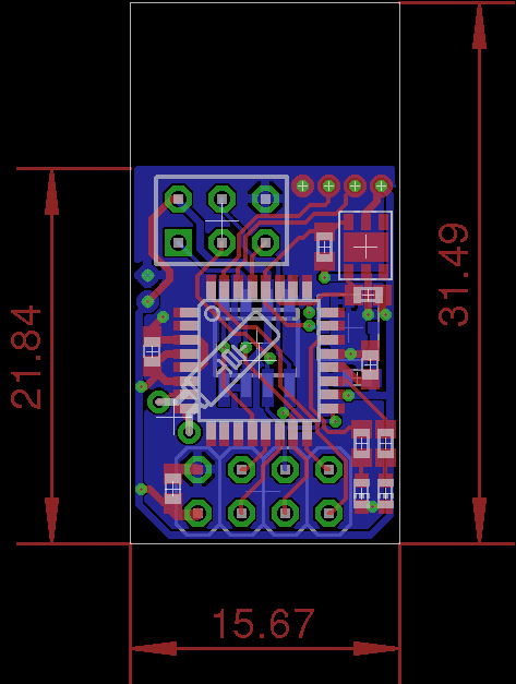
Right now, board dimensions with Si7021, 328p, spi flash, no stepup, is down to 15x21mm (smaller than the radio module). Might throw in a footprint for bmp180 as well, so I could equip one of the sensors with barometric sensor.. The complete sensor could fit on the end of a 2xAA battery holder (they are roughly 15x32x60mm).
-
Right now, board dimensions with Si7021, 328p, spi flash, no stepup, is down to 15x21mm (smaller than the radio module).
Nice, that sounds really like a minimal module!
-
Sounds very interesting! Though personally I'd rather have a good regulator / boost (even if it is in a separate module) than having to source particular components that will run at 1.8V.
How do you plan to integrate the nrf24? The "standard" or the "mini" version?
I would love it if the MySensors web site could have a department of open source pcb schematics just like it has models for 3D printing.
Soldering sounds tricky, you'd either have to reflow or heat the underside of the DFN6 on the pcb. With extra flux and paste.
-
i'm also making my own sensor right now and the si7021 is very interesting for removing my BIG dht11. But for home made soldering, the center ground pad should be soldered or it's not necessary?
@Tibus said:
But for home made soldering, the center ground pad should be soldered or it's not necessary?
To my best knowledge, there is no "center ground pin" on the Si7021? Or I have missed something. A friend of mine got a couple of them for another project, so I'll check up with him on the physical appearance, next time we get together.
@bjornhallberg said:
Sounds very interesting! Though personally I'd rather have a good regulator / boost (even if it is in a separate module) than having to source particular components that will run at 1.8V.
Btw. pricewise, comparing DHT22 and Si7021 they are about the same price (ebay price on DHT22, and mouser price for Si7021). So for sourcing DS18b20/DHT22, or sourcing the Si7021, is not that big a difference. I also can skip the stepup converter, and save a couple of $ there..
How do you plan to integrate the nrf24? The "standard" or the "mini" version?
It's the standard version, piggybacking on the minisensor. Actually (on the nrf24 modules that I have), the component area is 15x20mm (excluding the antenna part) So my arduino-clone could fit without "covering" the antenna..
I would love it if the MySensors web site could have a department of open source pcb schematics just like it has models for 3D printing.
That would be great.. :)
Anyway, I'll take a few more stabs at the schematic / layout before I publish it here..
-
Sounds very interesting! Though personally I'd rather have a good regulator / boost (even if it is in a separate module) than having to source particular components that will run at 1.8V.
How do you plan to integrate the nrf24? The "standard" or the "mini" version?
I would love it if the MySensors web site could have a department of open source pcb schematics just like it has models for 3D printing.
Soldering sounds tricky, you'd either have to reflow or heat the underside of the DFN6 on the pcb. With extra flux and paste.
@bjornhallberg said:
I would love it if the MySensors web site could have a department of open source pcb schematics just like it has models for 3D printing.
Yes, I would gladly create a section for this on the main site. But maybe we could start a pinned thread linking the once available?
-
Yes there is a TGnd Pad in the middle :
http://www.silabs.com/Support Documents/TechnicalDocs/Si7021.pdf
page 26... But I'll buy a Hot Air soldering station, i'll be easier to solder no?@Tibus Or perhaps you have a hot air gun in the toolbox. Not as elegant but it might do.
I'd much rather not try hot air (only have this at my disposal) and instead try to get at the pad from the backside of the pcb:
http://www.eevblog.com/forum/projects/soldering-dfn-and-qfn-devices/
With flux and paste possibly it should be quite easy. And besides, you'd need flux and/or paste for hot air reflow as well. -
Schematic as it is at the moment:
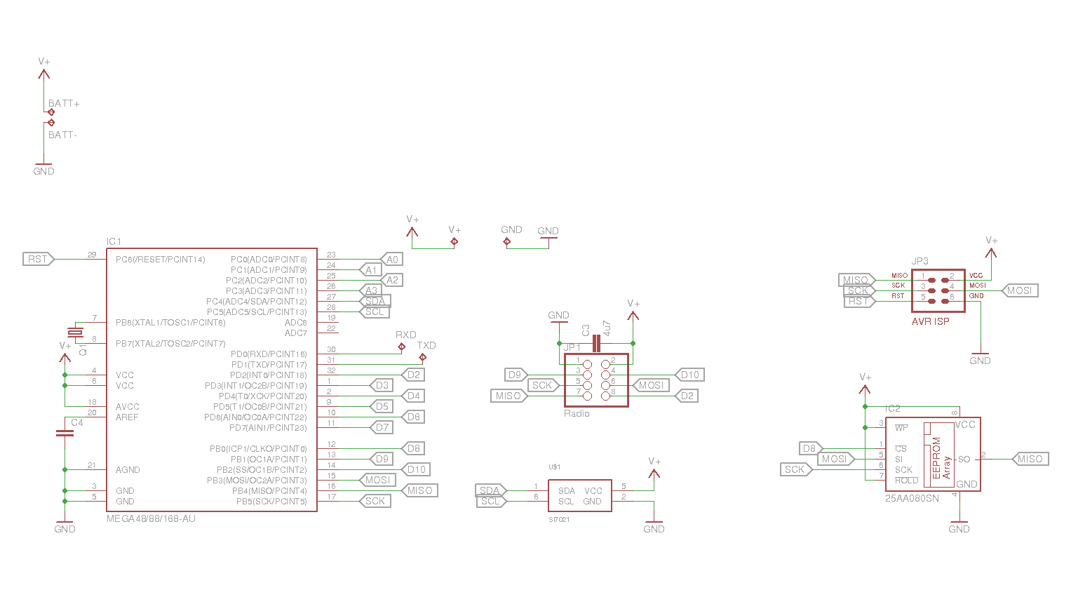
And the board as it is right now
I know it says eeprom for IC2, but the footprint is the same for SPI flashes.
the eeprom is placed on the bottom layer. Also, the nrf24 is placed on the bottom (so the eeprom is "in the middle of the sandwich". The dimensions of the total board will be about 15x30mm. This is the same size as the radio module. The empty area on the top is the area below the antenna.
Still need to make changes to the DFN package (upper right). and make a footprint for a bmp180 barometric sensor (and find a good home for it on the board).
Also, need to tidy up the routing, I used the autorouter which is very bad at placing the traces (haven't got any better since I used eagle the last time 11 years ago..) So maybe I just end rip everything up and hand route it by hand (this is the fun part of pcb designs, trying to mingle everything in to place :) thinking about the things my teacers told me 20 years ago about PCB design (oh f*ck I feel like an old geezer now! :))
Oh yeah, btw. there is also made room for a crystal (32Khz) on there.
-
This will be a very small board indeed! Not an expert but couldn't the radio interfere with MCU at these short distances?
It would be more the other way arround. The MCU is making trouble for the receive path of the radio module. But the radio module has a large gnd plane on the bottom towards the mcu board, so it should be shielded.
-
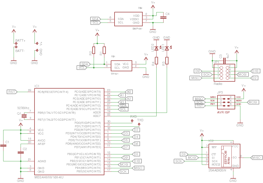
A new schematic / layout
I'm almost ready for sending it off to China, and get some boards back :)
Changes since last:
2 LED's added (figured debug output could be nice)
pullups added on i2c bus
caps changed to 0603 footprint
added a couple of extra caps for decoupling (MCU)
Added BMP180 barometric sensor (only need 1 node with this one though)
Moved components arround, squeezing things a little bit more together.
Routed manually this time, not that big a board, so no need to use the autorute functionTestpads on upper right corner of the pcba is GND, RXD/TXD and VCC, again nice to have serial available for debugging the first couple of boards.
Board is designed with dirtypcbs.com in mind for production (Used their DRU file in eagle to check things).
Schematic:
and pcb layout:
-
Fantastic! But I agree that is is perhaps a bit odd to have a footprint for a BMP180 on every board. You'll get a lot of boards when ordering 10x 5x5cm PCBs.
0603 ... time to get soldering. Haha. But those solder pads look pretty big actually. Is this the issue where Eagle actually makes 0603 caps more solderable than 0805 by making the pads longer?
@bjornhallberg said:
Fantastic! But I agree that is is perhaps a bit odd to have a footprint for a BMP180 on every board. You'll get a lot of boards when ordering 10x 5x5cm PCBs.
I know, but I thought that I just as well could put one in there when I was designing the pcb. Otherwise I would have to get it on an external pcb (sparkfun sells bmp180 breakut boards). And there was room for it :)
0603 ... time to get soldering. Haha. But those solder pads look pretty big actually. Is this the issue where Eagle actually makes 0603 caps more solderable than 0805 by making the pads longer?
Don't know, last time I used eagle (about 10 years ago) I made layouts with 0805 components, (and an atmega8). Actually I think that the board I made back then is still being used in production.
/Thomas
-
Any thoughts on how to panelize it? You'd get like six boards on a 5x5 if those dimensions hold? Perhaps you could do some alternative layouts for different sensors? I understand dirtypcbs no longer do grooving (if they ever did) ... how much pcb space is lost to routing typically?
In case anyone else is wondering about dirtypcbs, they seem to do an ok job typically:
http://lab.kjlr.dk/p/handystick
http://hackers.gallery/236/electronics/pcb-itead-studio-vs-dirtypcbs