Powering mote 24/7 using only a supercap and solar
-
@NeverDie said:
https://www.tindie.com/products/onehorse/bq25504-solar-cell-lipo-charger/
I ordered the OSH PARK boards, but I also ordered one of the pre-made BC25504 boards from Tindie (https://www.tindie.com/products/onehorse/bq25504-solar-cell-lipo-charger/). Considering that it's already fully assembled, and considered how much time it took me to layout the LTC3105 board, I think the price isn't unreasonable. If it "just works" right out of the box, then it's worth it to me. Also, the OSH PARK boards will take about two weeks to arrive. Hopefully the Tindie arrives a lot sooner than that. If I like it, then I'll order the BC25504 components from Digikey, which should arrive quickly.
Anyone else here used or tried the BC25504?
@NeverDie said:
@NeverDie said:
https://www.tindie.com/products/onehorse/bq25504-solar-cell-lipo-charger/
I ordered the OSH PARK boards, but I also ordered one of the pre-made BC25504 boards from Tindie (https://www.tindie.com/products/onehorse/bq25504-solar-cell-lipo-charger/). Considering that it's already fully assembled, and considered how much time it took me to layout the LTC3105 board, I think the price isn't unreasonable. If it "just works" right out of the box, then it's worth it to me. Also, the OSH PARK boards will take about two weeks to arrive. Hopefully the Tindie arrives a lot sooner than that. If I like it, then I'll order the BC25504 components from Digikey, which should arrive quickly.
Anyone else here used or tried the BC25504?
To his credit, the Tindie seller shipped it the same day I ordered, and tracking shows I should be receiving the pre-made BC25504 board tomorrow. :)
-
@NeverDie said:
@NeverDie said:
https://www.tindie.com/products/onehorse/bq25504-solar-cell-lipo-charger/
I ordered the OSH PARK boards, but I also ordered one of the pre-made BC25504 boards from Tindie (https://www.tindie.com/products/onehorse/bq25504-solar-cell-lipo-charger/). Considering that it's already fully assembled, and considered how much time it took me to layout the LTC3105 board, I think the price isn't unreasonable. If it "just works" right out of the box, then it's worth it to me. Also, the OSH PARK boards will take about two weeks to arrive. Hopefully the Tindie arrives a lot sooner than that. If I like it, then I'll order the BC25504 components from Digikey, which should arrive quickly.
Anyone else here used or tried the BC25504?
To his credit, the Tindie seller shipped it the same day I ordered, and tracking shows I should be receiving the pre-made BC25504 board tomorrow. :)
-
I received the BQ25504 pre-made board from Tindie, and gosh it's small:
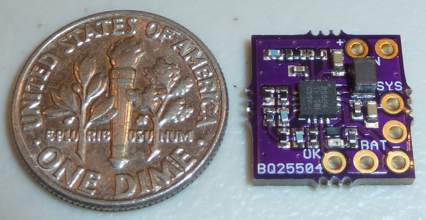
I guess my purchase of the PCB's from Osh Park was a waste, because I don't see how I could solder discrete parts which are that tiny. Any ideas?@NeverDie said:
I guess my purchase of the PCB's from Osh Park was a waste, because I don't see how I could solder discrete parts which are that tiny. Any ideas?
Reflow oven - http://makezine.com/2015/04/15/diy-open-source-reflow-oven/ As an aside, I just had lunch with Peter Easton last week, the inventor of ControlLeo, and he owns the DIY reflow oven market so you can't go wrong. Of course, I built one a couple years ago :+1:
-
The longest dimension of the discretes is about the height of the font on the "E pluribus unum" phrase of the dime. That's too tiny for me. I think I'll have to do my own board after all so that I may use larger components. 0603 is about as small as I want to go.
-
The Tindie board includes a tiny SMD LED which lights when Vbat_ok goes HIGH. So, in a room with dim indoor lighting, plugging just the cheap photovoltaic cell into the Tindie device makes the LED briefly flash about once every few seconds. The brighter the indoor light, the faster it flashes. Obviously, the act of flashing the LED drains the on-board storage capacitor, and the cycle repeats. I suppose simply counting the flashes might approximate a crude coulomb counter.
-
After playing around with the Tindie board, I think it's safe to say that for a low light energy harvesting application, having the LED on the board is a bug, not a feature because it rapidly throws away the harvested energy.
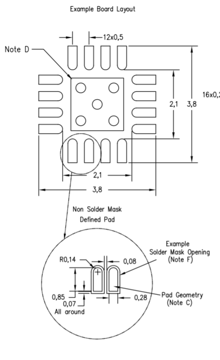
So, I'm making my own BQ25504 board. I'm pretty much done with Version 1, except that the land pattern (see attached) may be a little tricky to do in Diptrace because the pads are not purely rectangle nor purely circular.
-
i think simple pads should work. But sure it's better to follow recommanded footprint, that can avoid some short during soldering, and is also especially important when using stencils. This kind of shape can help for escaping solder during the process.
That said, I'm using Eagle...and already did mine :)
without led of course!I think in parameters you will also need to know how long take your capa to charge (if you want to press twice), what capa voltage range needed regarding bq25504 setup res etc.. I still think indoor it would need a little additional bat, because if it's a mote, lot of chance you could press once, and then wait for x sec/min before pushing again. especially if signing enabled. but perhaps you don't need signing with your mote..
I hope this helps :)
Edit: i updated the pic with the bottom. but if you want i can share gerbers if you want, as you're using diptrace
@scalz
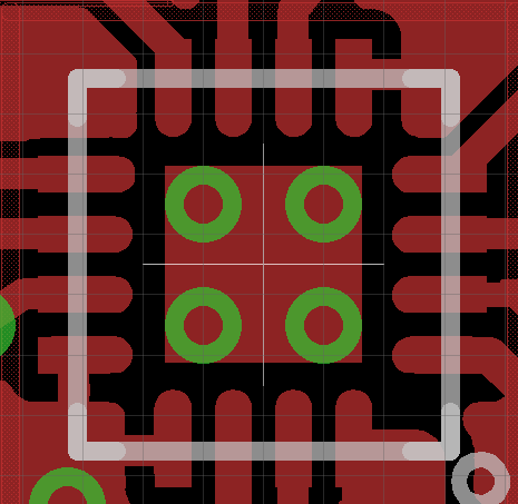
Are you connecting your BQ25504 thermal pad to anything on the other side of the board using the via holes? I tentatively connected mine to the large copper ground pour on the other side of the board, on the theory that doing so would help dissipate heat. -
@NeverDie nope. just copper on bottom. ground return through your powerpad, in this case, can give less perf.
-
@NeverDie nope. just copper on bottom. ground return through your powerpad, in this case, can give less perf.
Yesterday it was sunny outside, and the indoor ambient light was plenty for driving the BQ25504. Today, in stark contrast, it's very overcast outdoors, and the BQ25504 is really struggling. Input voltage from the PV cell with the BQ25504 as the load is hovering around 0.5v or 0.6v. Just a preliminary observation, but I'm not sure the BQ25504 will be useful at input voltages less than about 0.7v. Or maybe the Tiindie board cut some corners or something. I'll have a better idea after I make my own board and compare its performance against the Tindie board.
-
@NeverDie nope. just copper on bottom. ground return through your powerpad, in this case, can give less perf.
@scalz said:
@NeverDie nope. just copper on bottom. ground return through your powerpad, in this case, can give less perf.
Are you using tented via's? Because otherwise, it looks as though your thermal pad is electrically connected to the "just copper" on the bottom. But I guess you're not referring to the "just copper" as "ground" because it's not being used as a return path per se? Looking at the "Recommended Layout" (Figure 34 on page 26 of the datasheet), I see it refers to a "Top BND" and a "Bottom GND."
At the moment I'm not sure what to do, so I changed from having almost the entire bottom connected to ground to just creating an equivalent thermal pad on the bottom that's the same size as on the top, which is electrically connected via the 5 via's. I haven't specified that the via's be electrically isolated from the top thermal pad, because in the TI diagram (which I posted above) it doesn't appear that they are.
-
Problem solved. Looking more closely at the datasheet's "recommended layout," regular oval pads should be fine:
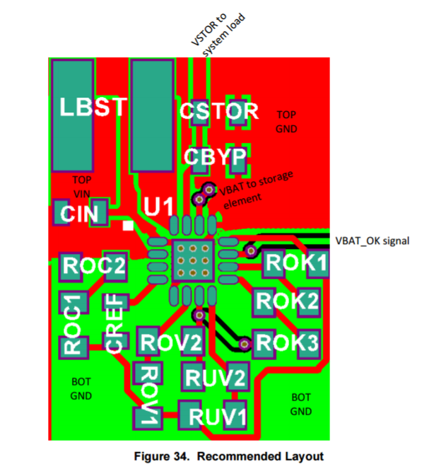
So, no need to go exotic on the pad geometry. I can't tell from looking at it whether the thermal pad on the bottom is isolated from "bottom GND" or not, though. -
Problem solved. Looking more closely at the datasheet's "recommended layout," regular oval pads should be fine:
So, no need to go exotic on the pad geometry. I can't tell from looking at it whether the thermal pad on the bottom is isolated from "bottom GND" or not, though. -
This post is deleted!
-
This post is deleted!
-
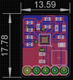
Here's what I'm going with for now:
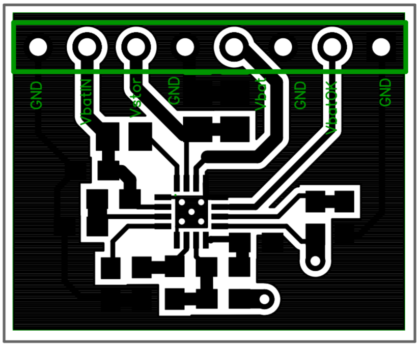
As you can see, this one uses only one ground plane. Board size is 22mmx18mm. It uses 0603 and 0805 discrete parts, which for me makes it easier to hand solder. The only tricky part to hand solder will be the BQ25504 itself, but there's nothing I can do about that.
-
@NeverDie
sorry for delay..
i have a pad on bottom but it's not grounded on the bottom side. the power pad is grounded only on top. i don't remember but you should have a layout guideline included with the circuit footprint, for explaining.
i also use 0603/0805. -
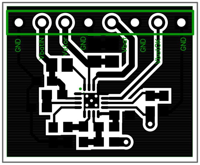
I guess my oval pads reverted to the default pattern when I re-synced with the schematic. So, fixing that again, here's what I'm going with:
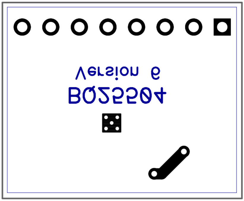
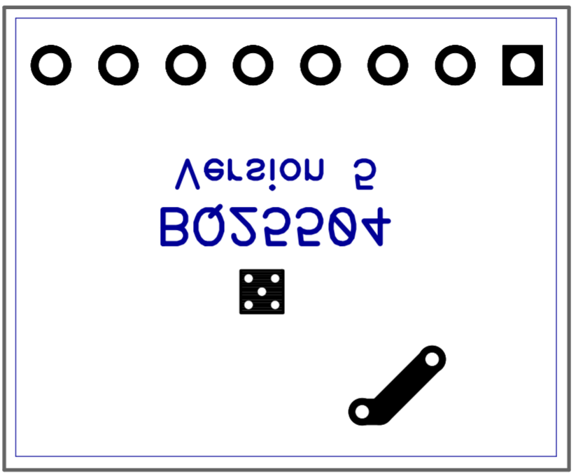
There's a bit more clean-up I should probably do, but I need to learn a bit more about Diptrace before I can do it. Meanwhile, I sent Version 6 to the fab, since fabbing is the critical path. -
@NeverDie
sorry for delay..
i have a pad on bottom but it's not grounded on the bottom side. the power pad is grounded only on top. i don't remember but you should have a layout guideline included with the circuit footprint, for explaining.
i also use 0603/0805. -