Powering mote 24/7 using only a supercap and solar


  • Hero Member

    Anyone already doing it?

    Seems like all that's needed is a supercap with low enough leakage current such that harvested solar energy exceeds leakage current per 24 hour cycle.

    Yesterday I ordered a few boost converters to play around with: an AAT1217, an LTC3105, an MP3418, and an L6920DTR. Out of those four different boost converters, hopefully at least one will prove adequate. Maybe all of them will. Either way, I'm sure to learn something about what's ultimately needed.

    I checked the unloaded voltage on an el cheapo solar cell (scavanged from a $1 garden light), and it came out around 1v under indoor ambient light conditions, near a window on a darkly overcast, rainy day with no indoor lights on. That's higher than what I was expecting. Of course, how much of that is ephemeral and how much of it is solid under load remains to be seen, and I guess that's part of what I'll be learning.

    alt text
    alt text
    alt text
    For illustration purposes, I put a little TH mote inside it.


  • Hero Member

    For a blocking diode, I'll probably use this: http://www.digikey.com/product-detail/en/toshiba-semiconductor-and-storage/CUS520,H3F/CUS520H3FCT-ND/5114381
    because it's only 21 cents, quantity 1. 280mv forward voltage drop. At most 1uA reverse flow current.

    That said, a more interesting (though a lot more expensive) choice would be: http://www.ti.com/lit/ds/symlink/sm74611.pdf
    which has a forward voltage drop of just 28mv, and a similar maximum reverse current.


  • Hardware Contributor

    one of the best part i know for this is also the BQ25504. One of the most efficient i think.
    I'm designing a board for solar 😉 so i've studied a bit alternatives for my usecase.
    Best is to fit an app, because there are always lot of dilemma and compromise regarding solar panel used, input voltage, effiency not always the same with MPPT, and cost...not so simple,
    There are also multiple solar charger boards which exist like the adafruit or the lipo rider, more simple but can do the job too etc...
    Lot of articles about this on internet too.
    These low input voltage are nice, but it's not a big harvest. for indoor, with all packet exchange we have for a transmission can be critical. Then you can do battery extender etc.. but add cost.
    For outdoor a bit easier, and perhaps does not need expensive ic to run etc..


  • Hero Member

    @scalz said:

    one of the best part i know for this is also the BQ25504. One of the most efficient i think.
    I'm designing a board for solar 😉 so i've studied a bit alternatives for my usecase.
    Best is to fit an app, because there are always lot of dilemma and compromise regarding solar panel used, input voltage, effiency not always the same with MPPT, and cost...not so simple,
    There are also multiple solar charger boards which exist like the adafruit or the lipo rider, more simple but can do the job too etc...
    Lot of articles about this on internet too.
    These low input voltage are nice, but it's not a big harvest. for indoor, with all packet exchange we have for a transmission can be critical. Then you can do battery extender etc.. but add cost.
    For outdoor a bit easier, and perhaps does not need expensive ic to run etc..

    Yeah, the BQ25504 does appear to offer nice functionality. But at 3x3mm in size, I'm afraid it would be challenging to solder it. Is it available in a larger package or pre-soldered onto a breakout board?


  • Hero Member

    Well, answering my own question, it looks as though there is at least one breakout board for it: https://www.tindie.com/products/onehorse/bq25504-solar-cell-lipo-charger/
    Sticker shock though.

    Also, there's this breakout based on the LTC3108, but be prepared for sticker shock again: https://www.crispytronics.com/collections/energy-harvesting/products/energy-harvester-breakout-100-mv-startup?variant=882155101


  • Hardware Contributor

    yep i know these, look nice 😉 all depends of the usecase like i said


  • Hero Member

    I'm quite impressed with Digikey. I ordered the above parts on Tuesday (2 days ago), for just regular First Class mail delivery, and the parts arrived today already. Cool!

    Anyhow, all these parts are so small that I'll need to create some custom breakout boards for each of them in order to do any testing. I do hope that regular tack and drag hand soldering works on parts this small. Otherwise, I'll have to build a reflow oven out of a toaster oven, and that might mean further delay.


  • Hero Member

    @NeverDie said:

    @scalz said:

    one of the best part i know for this is also the BQ25504. One of the most efficient i think.
    I'm designing a board for solar 😉 so i've studied a bit alternatives for my usecase.
    Best is to fit an app, because there are always lot of dilemma and compromise regarding solar panel used, input voltage, effiency not always the same with MPPT, and cost...not so simple,
    There are also multiple solar charger boards which exist like the adafruit or the lipo rider, more simple but can do the job too etc...
    Lot of articles about this on internet too.
    These low input voltage are nice, but it's not a big harvest. for indoor, with all packet exchange we have for a transmission can be critical. Then you can do battery extender etc.. but add cost.
    For outdoor a bit easier, and perhaps does not need expensive ic to run etc..

    Yeah, the BQ25504 does appear to offer nice functionality. But at 3x3mm in size, I'm afraid it would be challenging to solder it. Is it available in a larger package or pre-soldered onto a breakout board?

    I've changed my mind. I want to try the BQ25504. Why? Well, it turns out a guy in Switzerland has already done more or less the experiment that I was going to do, and this is his conclusion:
    alt text
    (http://www.limpkin.fr/index.php?post/2011/12/07/Indoor-solar-energy-harvesting%3A-a-platform-to-(finally)-get-some-numbers)

    LOL. So, regardless of soldering difficulty, the BQ25504 looks like it's sufficiently better that it's worth pursuing.

    However, TI's eval board for the BQ25504, is a totally insane $99. So, it's either DIY, or else find some other BQ25504 board that's priced more sensibly. There is one on Tindie that I've already mentioned (above). Any others worth considering?


  • Hero Member

    Fortunately, I notice that the author of the Tindie product has posted his PCB on OSH PARK: https://www.oshpark.com/shared_projects/tksisJZ6 An order for 3 PCB's costs a total of just $1.25. Nice!


  • Hero Member

    As for soldering the BQ25504 chip, must I use a reflow oven, or will careful hand soldering (e.g. tack and reflow) be effective?


  • Hero Member

    OSH PARK is the gift that keeps on giving. I found an even simpler BQ25504 breakout board here: https://oshpark.com/shared_projects/CYdxpE9S
    Costs just $0.65 for 3 boards.
    The design files are here: https://github.com/bootchk/BQStripped


  • Admin

    @NeverDie And bootchk designed it using KiCAD - well done! As a side note, in the very early days of the MySensors core team (@hek, @tbowmo, @Anticimex and I) decided that, in the spirit of open source, to abandon commercial / proprietary CAD programs for the MySensors official board designs, hence why SenseBender Micro is in KiCAD and the forthcoming gateway will be too. We wanted to ensure that all board designs would be available to users freely for modification and improvements. While KiCAD is the standard for the official MySensors board designs, it would be nice to see broader adoption by the MySensors community as well (as I step down from my soapbox) 😉


  • Mod

    @NeverDie said:

    As for soldering the BQ25504 chip, must I use a reflow oven, or will careful hand soldering (e.g. tack and reflow) be effective?

    At first sight the footprint looks identical to that of nrf24 (on phone, so didn't check).
    These can be handsoldered, with a fine soldering tip.


  • Hero Member

    @NeverDie said:

    https://www.tindie.com/products/onehorse/bq25504-solar-cell-lipo-charger/

    I ordered the OSH PARK boards, but I also ordered one of the pre-made BC25504 boards from Tindie (https://www.tindie.com/products/onehorse/bq25504-solar-cell-lipo-charger/). Considering that it's already fully assembled, and considered how much time it took me to layout the LTC3105 board, I think the price isn't unreasonable. If it "just works" right out of the box, then it's worth it to me. Also, the OSH PARK boards will take about two weeks to arrive. Hopefully the Tindie arrives a lot sooner than that. If I like it, then I'll order the BC25504 components from Digikey, which should arrive quickly.

    Anyone else here used or tried the BC25504?


  • Hero Member

    @blacey said:

    @NeverDie And bootchk designed it using KiCAD - well done! As a side note, in the very early days of the MySensors core team (@hek, @tbowmo, @Anticimex and I) decided that, in the spirit of open source, to abandon commercial / proprietary CAD programs for the MySensors official board designs, hence why SenseBender Micro is in KiCAD and the forthcoming gateway will be too. We wanted to ensure that all board designs would be available to users freely for modification and improvements. While KiCAD is the standard for the official MySensors board designs, it would be nice to see broader adoption by the MySensors community as well (as I step down from my soapbox) 😉

    I'm using Diptrace, but it isn't very good for sharing source files with other users, not even other Diptrace users. Doing so involves some rather cumbersome export and inport of components and patterns, and then re-linking the two afterward. On the plus side, though, it was very easy to learn. Anyhow, it seems that all the major PCB design tools have free versions for hobbyists. Hopefully if you know one, it's much easier to learn another if the need arises.


  • Hero Member

    @Yveaux said:

    @NeverDie said:

    As for soldering the BQ25504 chip, must I use a reflow oven, or will careful hand soldering (e.g. tack and reflow) be effective?

    At first sight the footprint looks identical to that of nrf24 (on phone, so didn't check).
    These can be handsoldered, with a fine soldering tip.

    Thanks! Your optimistic post motivated me to pull the trigger on ordering the OSH PARK boards.


  • Hardware Contributor

    @NeverDie
    good choice 😉
    i also read this article. i have some BQ25504 sample, but for the moment i'm not using (even if i did the eval board!) as it was not fitting my usecase, and cost goals. And for a simple button mote, i would prefer a power supply without regulator...enough years lifetime for me and no additional cost with ic + supercap (which need to be mF or F!) + solar cell (and it's size even for small). Add to this that sun/light exposure/placement is critical indoor or harvesting nothing.

    Another sidenote, we also need to take in account the power it needs for packet transmission including retries + signing (which can be n*100ms..). no problem if there is an additional batt or if it's a simple sensor without ack. otherwise, it may need an additional batt in the cost.

    But it's still a cool ic, nice project 🙂


  • Hero Member

    @NeverDie said:

    @NeverDie said:

    https://www.tindie.com/products/onehorse/bq25504-solar-cell-lipo-charger/

    I ordered the OSH PARK boards, but I also ordered one of the pre-made BC25504 boards from Tindie (https://www.tindie.com/products/onehorse/bq25504-solar-cell-lipo-charger/). Considering that it's already fully assembled, and considered how much time it took me to layout the LTC3105 board, I think the price isn't unreasonable. If it "just works" right out of the box, then it's worth it to me. Also, the OSH PARK boards will take about two weeks to arrive. Hopefully the Tindie arrives a lot sooner than that. If I like it, then I'll order the BC25504 components from Digikey, which should arrive quickly.

    Anyone else here used or tried the BC25504?

    To his credit, the Tindie seller shipped it the same day I ordered, and tracking shows I should be receiving the pre-made BC25504 board tomorrow. 🙂


  • Hero Member

    I received the BQ25504 pre-made board from Tindie, and gosh it's small:
    0_1479601957884_BQ25504_pesky.jpg
    I guess my purchase of the PCB's from Osh Park was a waste, because I don't see how I could solder discrete parts which are that tiny. Any ideas?


  • Admin

    @NeverDie said:

    I guess my purchase of the PCB's from Osh Park was a waste, because I don't see how I could solder discrete parts which are that tiny. Any ideas?

    Reflow oven - http://makezine.com/2015/04/15/diy-open-source-reflow-oven/ As an aside, I just had lunch with Peter Easton last week, the inventor of ControlLeo, and he owns the DIY reflow oven market so you can't go wrong. Of course, I built one a couple years ago 👍


  • Hero Member

    The longest dimension of the discretes is about the height of the font on the "E pluribus unum" phrase of the dime. That's too tiny for me. I think I'll have to do my own board after all so that I may use larger components. 0603 is about as small as I want to go.


  • Hero Member

    The Tindie board includes a tiny SMD LED which lights when Vbat_ok goes HIGH. So, in a room with dim indoor lighting, plugging just the cheap photovoltaic cell into the Tindie device makes the LED briefly flash about once every few seconds. The brighter the indoor light, the faster it flashes. Obviously, the act of flashing the LED drains the on-board storage capacitor, and the cycle repeats. I suppose simply counting the flashes might approximate a crude coulomb counter.


  • Hero Member

    After playing around with the Tindie board, I think it's safe to say that for a low light energy harvesting application, having the LED on the board is a bug, not a feature because it rapidly throws away the harvested energy.

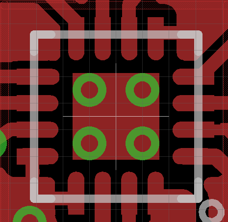
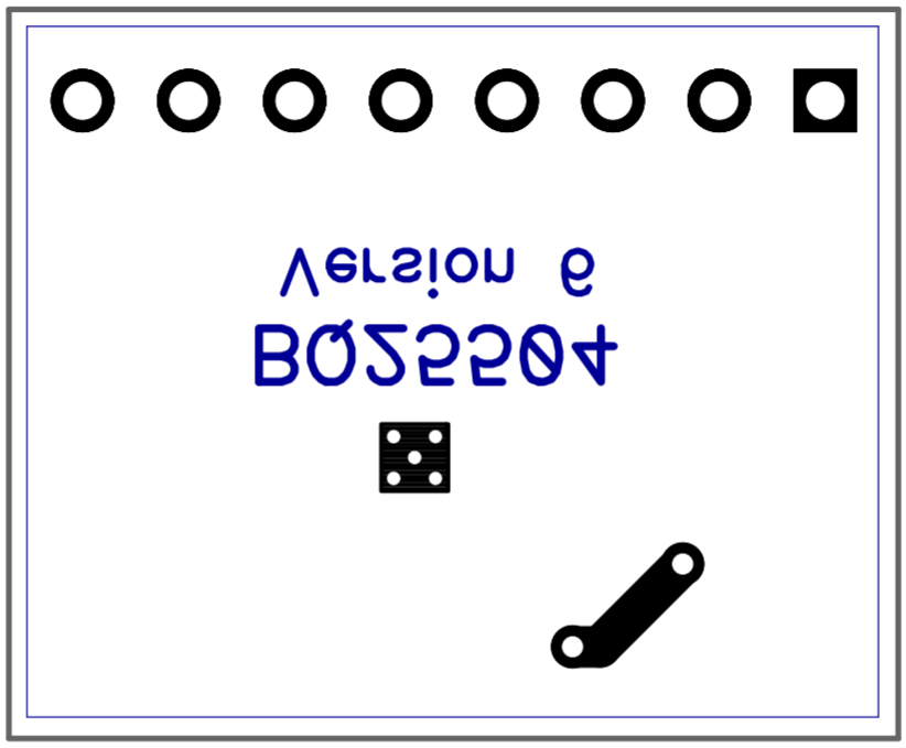
    So, I'm making my own BQ25504 board. I'm pretty much done with Version 1, except that the land pattern (see attached) may be a little tricky to do in Diptrace because the pads are not purely rectangle nor purely circular.

    0_1479826876695_land_pattern.png


  • Hardware Contributor

    i think simple pads should work. But sure it's better to follow recommanded footprint, that can avoid some short during soldering, and is also especially important when using stencils. This kind of shape can help for escaping solder during the process.

    That said, I'm using Eagle...and already did mine 🙂
    0_1479833474563_bq25504 footprint.png
    0_1479842780247_bq25504_eval.png
    without led of course!

    I think in parameters you will also need to know how long take your capa to charge (if you want to press twice), what capa voltage range needed regarding bq25504 setup res etc.. I still think indoor it would need a little additional bat, because if it's a mote, lot of chance you could press once, and then wait for x sec/min before pushing again. especially if signing enabled. but perhaps you don't need signing with your mote..

    I hope this helps 🙂

    Edit: i updated the pic with the bottom. but if you want i can share gerbers if you want, as you're using diptrace


  • Hero Member

    @scalz
    Are you connecting your BQ25504 thermal pad to anything on the other side of the board using the via holes? I tentatively connected mine to the large copper ground pour on the other side of the board, on the theory that doing so would help dissipate heat.


  • Hardware Contributor

    @NeverDie nope. just copper on bottom. ground return through your powerpad, in this case, can give less perf.


  • Hero Member

    Yesterday it was sunny outside, and the indoor ambient light was plenty for driving the BQ25504. Today, in stark contrast, it's very overcast outdoors, and the BQ25504 is really struggling. Input voltage from the PV cell with the BQ25504 as the load is hovering around 0.5v or 0.6v. Just a preliminary observation, but I'm not sure the BQ25504 will be useful at input voltages less than about 0.7v. Or maybe the Tiindie board cut some corners or something. I'll have a better idea after I make my own board and compare its performance against the Tindie board.


  • Hero Member

    @scalz said:

    @NeverDie nope. just copper on bottom. ground return through your powerpad, in this case, can give less perf.

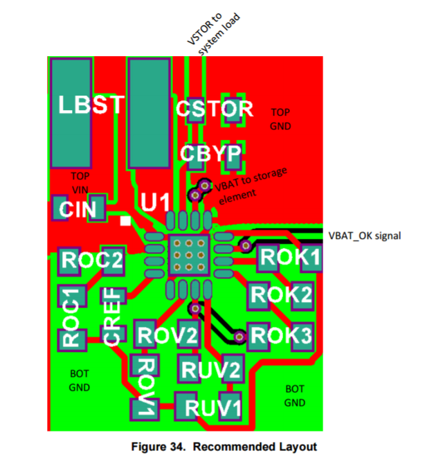
    Are you using tented via's? Because otherwise, it looks as though your thermal pad is electrically connected to the "just copper" on the bottom. But I guess you're not referring to the "just copper" as "ground" because it's not being used as a return path per se? Looking at the "Recommended Layout" (Figure 34 on page 26 of the datasheet), I see it refers to a "Top BND" and a "Bottom GND."

    At the moment I'm not sure what to do, so I changed from having almost the entire bottom connected to ground to just creating an equivalent thermal pad on the bottom that's the same size as on the top, which is electrically connected via the 5 via's. I haven't specified that the via's be electrically isolated from the top thermal pad, because in the TI diagram (which I posted above) it doesn't appear that they are.


  • Hero Member

    Problem solved. Looking more closely at the datasheet's "recommended layout," regular oval pads should be fine:
    0_1479917570580_oval.png
    So, no need to go exotic on the pad geometry. I can't tell from looking at it whether the thermal pad on the bottom is isolated from "bottom GND" or not, though.


  • Hero Member

    This post is deleted!

  • Hero Member

    This post is deleted!

  • Hero Member

    This post is deleted!

  • Hero Member

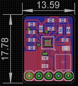
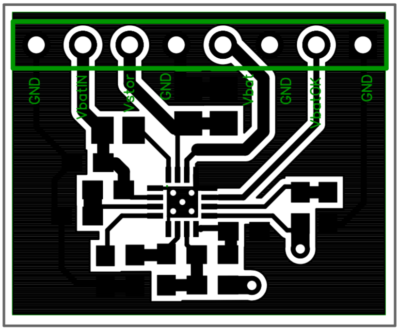
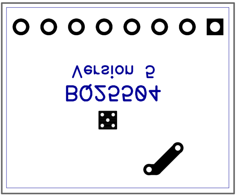
    Here's what I'm going with for now:
    0_1479924552790_BQ25504_v5_top.png
    0_1479924566770_BQ25504_v5_bottom.png

    As you can see, this one uses only one ground plane. Board size is 22mmx18mm. It uses 0603 and 0805 discrete parts, which for me makes it easier to hand solder. The only tricky part to hand solder will be the BQ25504 itself, but there's nothing I can do about that.


  • Hardware Contributor

    @NeverDie
    sorry for delay..
    i have a pad on bottom but it's not grounded on the bottom side. the power pad is grounded only on top. i don't remember but you should have a layout guideline included with the circuit footprint, for explaining.
    i also use 0603/0805.


  • Hero Member

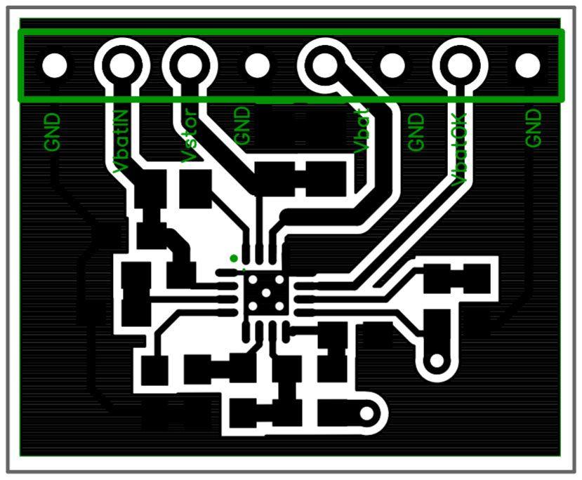
    I guess my oval pads reverted to the default pattern when I re-synced with the schematic. So, fixing that again, here's what I'm going with:
    0_1479927030669_BQ25504_v6_top.png
    0_1479927049360_BQ25504_v6_bottom.png
    There's a bit more clean-up I should probably do, but I need to learn a bit more about Diptrace before I can do it. Meanwhile, I sent Version 6 to the fab, since fabbing is the critical path.


  • Hero Member

    @scalz said:

    i also use 0603/0805.

    In that case, if you want to post your fab files, I can post mine. Then we can have a healthy competition to see whether they work the same or whether one works better than the other.


  • Hardware Contributor

    @NeverDie
    oh, no competition... or let me win please 😆 I'm joking. that said i'm not sure, but I think i see Wally on your board 😉
    I'm back in an hour for sharing. i need to assemble few boards for myself 🙂


  • Hero Member

    @scalz said:

    i'm not sure, but I think i see Wally on your board 😉

    LOL. You probably need better ventilation when you're soldering. The fumes are getting to you. 😆


  • Hero Member

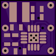
    Interestingly, in today's mail I received the "BQ25504 Stripped" PCB
    alt text
    https://oshpark.com/shared_projects/CYdxpE9S

    that I ordered on November 16. That's about twice faster than their normal turnaround speed when I send them new fab files. The board itself is noticeably smaller than the Tindie board.


  • Hardware Contributor

    @NeverDie said:

    @scalz said:

    i'm not sure, but I think i see Wally on your board 😉

    LOL. You probably need better ventilation when you're soldering. The fumes are getting to you. 😆

    😆 no fumes tonight, reflow oven working for me 🙂

    Wally is in your GND pour, in each of your board I think.
    I mean you should not have any gnd around some settings resistors and capa.
    Check carefully the section 11.1 Layout Guidelines in datasheet.
    This is why on the reference layout you see Top GND only on half board. Or then it may happen less performance depending of mutliple factors.
    It's also explained how to route the GND.

    That said, in case it can help, here is my gerbers https://www.dropbox.com/s/tugdbc3cfrlmdu7/bq25504_gerbers.rar?dl=0

    Enjoy


  • Hero Member

    @scalz

    What is "Wally"? I haven't heard that term before, and it's not in the datasheet either. I thought you were jokingly making an obscure reference to Waldo, as in "Where's Waldo?" That's why I had thought the fumes must have gotten to you. I realize now that Wally must instead be a French electrical term of some kind.

  • Hardware Contributor

    @NeverDie
    lol
    yep you were right, where's waldo/wally but where i live we say Charlie 🙂


  • Hero Member

    @scalz
    Sacrébleu. I just now tried sending your gerber files to OSH PARK, but it complains, " I can't find a board outline file." A fab will need a complete set of files to get anything done.


  • Hero Member

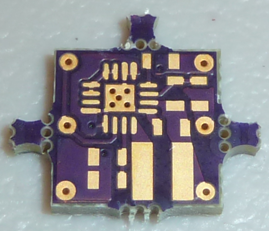
    In any event, the "stripped" BQ25504 board that I received yesterday looks rather disheveled:
    0_1479991946287_BQ25504_disheveled.jpg

    @scalz
    Do you see any Wally's in it?


  • Hardware Contributor

    @NeverDie
    ahah 🙂

    If it can help you, here it is : https://oshpark.com/shared_projects/XRsFBtzu
    This is because i've generated the gerbers with an other fabhouse CAM.
    In mine, GML is the dimension layer if i remember right.
    You can also open the gerbers in a viewer like Gerbv etc..
    For oshpark, i have modified it a little bit because of slightly different DRC.


  • Hero Member

    @scalz
    Thanks. I just now ordered it.

    Interestingly, if you look at Ti's eval board for the bq25504, they do in fact connect the top and bottom ground planes, and the thermal pad on the BQ25504 is connected to the entire bottom ground plane, not just another small thermal pad:

    https://www.ti.com/seclit/df/tidu094/tidu094.pdf


  • Hardware Contributor

    @NeverDie
    cool.
    Well, perhaps it's ok. I followed datasheet guidelines..no matter the powerpad is connected on top.

    Perhaps, you may need the schematic to know where parts are placed 😉
    0_1479989388027_sch.png
    You'll need to set your resistors of course.

    If really needed, no problem i can upload all the files..


  • Hero Member

    @scalz

    You should upload it to https://www.openhardware.io/ I'm sure a lot of people would find it very helpful.


  • Hero Member

    @scalz
    Out of curiosity, why did you choose such a large inductor? I notice that the "stripped" BQ25504 pcb (photo above) did the same thing. Are there advantages to the larger size?


  • Hero Member

    @NeverDie said:

    @scalz
    Out of curiosity, why did you choose such a large inductor? I notice that the "stripped" BQ25504 pcb (photo above) did the same thing. Are there advantages to the larger size?

    Nevermind. I see now from your schematic that you're using the coilcraft inductor from Table 1 of the DS.


  • Hero Member

    Interestingly, looking at the Tindie board now, it's clear based on its inductor's dimensions that the Tindie board is not using one of the Table 1 recommended inductors. Perhaps that explains why the Tindie board appears to be sucking wind at the lower voltages.


  • Hero Member

    @NeverDie
    Coilcraft doesn't seem very available in the US, but Wurth has a similar one that's still on the DS table list that's probably a good substitute: http://www.digikey.com/product-detail/en/wurth-electronics-inc/744031220/732-1012-1-ND/1639073

    Also, I'll have to update my board to use a larger inductor. I had blithely assumed, based on the Tindie board, that an 0805 would be sufficient, but now that I'm digging into it probably not.


  • Hero Member

    @NeverDie
    I take it back. The Wurth component I just referenced has a rather complex looking land pattern.

    Fortunately, the last remaining component on the Table 1 recommended list is a Wurth that has a much easier land pattern: http://www.digikey.com/product-detail/en/wurth-electronics-inc/744025220/732-2619-1-ND/2445718


  • Hardware Contributor

    @NeverDie
    yep from guidelines.
    but also because it's better to use shielded inductors for multiple reasons like EMI..and also good inductors and parts give better perf, efficiency etc.. lot of docs on this.

    That said, the footprint i use is also compatible with the 0805 advised in datasheet if i remember. it's possible to use both ref for the same footprint i've not the datasheet in front of me right now but width shoud be ok.


  • Hero Member

    It seems as though TI's evaluation board ignores the design recommendations given in the datasheet, in particular: "...it is highly recommended that no ground planes be poured near the voltage setting resistors or the sample and hold capacitor." In the case of the TI's evaluation board, virtually the entire bottom layer is a ground plane. I don't know what to make of that.

    Anyhow, I ordered the Wurth inductors. I also ordered a 3x3 QFN-16 solder stencil as some fallback insurance, as the BQ25504 looks like it will be very challenging to solder.


  • Hero Member

    Also, the layout guidelines say, " It is best to use vias and bottom traces for connecting the inductor to its respective pins instead of the capacitors." Yet, the recommended layout doesn't do that.


  • Hero Member

    Part of what's strange is the Recommended Layout (Figure 34 in the datasheet) shows pin 12 belonging to a different ground plane than pin 13. Yet, the schematic shows pins 12 and 13 wired directly together.

    @scalz
    Just where are the two different ground planes supposed to connect together? Or is one supposed to float relative to the other?


  • Hardware Contributor

    @NeverDie
    ok i'll put on my git&openhardware asap.

    about the planes, you're right. I've a little doubt. on most designs, it's directly to gnd. i understand about the layout guidelines. but the datasheet picture layout is a bit confusing, if it's internally connected or not..i'll check a bit later.

    good point 😉


  • Hero Member

    @scalz

    Section 11.1 says, "When laying out the non-power ground return paths (e.g. from resistors and CREF), it is recommended to use short traces as well, separated from the power ground traces and connected to AVSS pin 12. This avoids ground shift problems, which can occur due to superimposition of power ground current and control ground current. The PowerPad should not be used as a power ground return path."

    I think that's why in the Recommended Layout (Figure 34), pins 12 and 13 are not connected directly together. However, on your board, they are directly connected, probably because of the schematic.

    What do they mean by "The PowerPad"? Do they mean the thermal pad beneath the chip? Maybe that's another reason why pin 12 is not connected to the thermal pad in the Recommended Layout.

    I don't know what the right answer is. I'm just trying to make sense of what seem like inconsistencies in the datasheet.


  • Hero Member

    I suppose if worse came to worst, we could try answering the question empirically by using a test setup similar to this:

    0_1480288951886_BQ25504_v14_top.png
    0_1480288994462_BQ25504_v14_bottom.png

    In this instance I partitioned the data ground from the power ground, and the two are not connected. However, via the header pins, a jumper could be connected between the two grounds. The experiment would be to try it both ways--connected vs. unconnected--and see which performs better.


  • Hero Member

    The through holes on the stripped BQ25504 PCB (above)from Osh Park have too small a diameter to fit header pins into. In fact, it would require a very narrow gauge wire (narrower than what I have) to fit into it. So, unfortunately, I have doubts as to whether I will be able to test it, let alone use it.

    This is all rather disappointing. 😖 So far nothing about the BQ25504 has been easy.


  • Hero Member

    Not that it proves anything, but using KiCAD to look at the BQstripped PCB, I notice that the PCB designer chose to connect pins 12 and 13 both directly to each other and directly to the thermal pad.


  • Admin

    @NeverDie said:

    Not that it proves anything, but using KiCAD to look at the BQstripped PCB, I notice that the PCB designer chose to connect pins 12 and 13 both directly to each other and directly to the thermal pad.

    Did you say KiCAD? 👍 👍 👍


  • Hero Member

    @blacey said:

    Did you say KiCAD? 👍 👍 👍

    Yup. I had to use KiCAD to confirm the proper chip orientation before attempting to hand solder it to their PCB. Looks like a nice program.

    I had doubts I could hand solder the BQ25504, but I tried it using Dave Jones's tack and reflow method, and to my untrained eye it looks like it came out OK, despite the chip not being completely well aligned with the solder pads:
    0_1480378211590_BQ25504_1.jpg

    0_1480378225784_BQ25504_2.jpg

    0_1480378245176_BQ25504_3.jpg

    0_1480378270381_BQ25504_4.jpg

    The Wurth inductors arrived today, so I'll have a go at soldering that on next. Hopefully the BQstripped PCB designer picked the same one I did!


  • Hero Member

    Looks as though the inductor hand soldered as well:
    3_1480381576419_inductor4.jpg 2_1480381576419_inductor3.jpg 1_1480381576418_inductor2.jpg 0_1480381576418_inductor1.jpg


  • Hero Member

    Interestingly, if one looks at the KiCad schematic for the bqstripped PCB, you will notice that it draws a distinction between regular GND and GNDPWR:
    0_1480428663373_kicad_schematic.pdf

    However, as already noted, that distinction seems to be cast aside when they laid out the PCB traces, since pins 12 and 13 are connected together directly by a trace. Indeed, the schematic explicitly shows GNDPWR connected to GND. So, why create the distinction in the first place?


  • Hardware Contributor

    @NeverDie
    this is for the power gnd plane regarding the analog gnd plane. analog for instance should be connected at one point. but then in practice like you said it looks a bit different...
    don't worry too much i think!
    The good in this, is i think, you have learnt good things (taking care of datasheet guidelines etc...) for future 👍


  • Hero Member

    @scalz

    I want to do it properly. I'm just not sure what is proper with this chip. What is the technically correct way to do it?

    P.S. I ordered some 30AWG wire for hooking up the BQstripped PCB.


  • Hero Member

    I had to order some 4.7uF smd 0603 capacitors and 4.42M ohm 0603 resistors.

    The DS also calls for 15.62M ohm resistors, but the closest thing that Digikey carries is 15M ohm 0603 smd's, so that's what I ordered.

    Meanwhile I did solder the 10nf capacitors to the BQstripped pcb, as I had those on hand. If I had it to do over, I would probably have soldered them prior to soldering the BQ25504 and the 22uH inductor, as those parts were in the way.


  • Hero Member

    Just a few notes on a conservative approach to component selection for boost converters that I've lately gleaned from reading various datasheets:

    1. Ideally, capacitors should be rated X5R or X7R.

    2. For inductors, generally speaking the lower the DCR the better, provided that the saturation current remains appropriately high enough. For instance, the B82462G4 series (http://www.digikey.com/product-search/en/inductors-coils-chokes/fixed-inductors/196627?k= +B82462G4&k=&pkeyword= +B82462G4&pv7=2&mnonly=0&newproducts=0&ColumnSort=0&page=1&quantity=0&ptm=0&fid=0&pageSize=500 ) has much lower DCR than any of the datasheet recommended inductors. These inductors are more expensive, but their use should, in theory, lead to higher efficiency and/or lower start/operating voltages. Also, I suspect the Tindie board's performance is impaired by its choice of inductor, because I haven't seen specs on any inductors as small as theirs is that has a low DCR.


  • Hardware Contributor

    +1 for X5R/X7R 😉


  • Hero Member

    @scalz said:

    +1 for X5R/X7R 😉

    I looked into it a little bit more, and I'm defaulting to X7R for everything, unless there's good reason not to: https://www.maximintegrated.com/en/app-notes/index.mvp/id/5527 The article also provides good reason to favor larger package sizes, up to size 1210, if the design allows.


  • Hardware Contributor

    @NeverDie
    that's also what i do, ceramic, x7r everywhere when possible. nice article, thx for sharing 😉


  • Hero Member

    I've settled on this series of shielded inductor as having a good bang for buck ratio: low DCR, high current rating, and relatively low price: http://www.digikey.com/catalog/en/partgroup/dg-series/53965?mpart=1255AY-220M=P3&vendor=490

    If anyone knows of a better series than that one, please post.


  • Hero Member

    For comparison, I ordered an inexpensive ($0.91, including shipping) 6v panel: https://www.aliexpress.com/item/6V-0-6W-Solar-Power-Panel-Module-DIY-Small-Cell-Charger-For-Light-Battery-Phone-Toy/32723002222.html?spm=2114.13010608.0.0.OYll8L

    It's a little bigger, but still reasonably small (a little more than 2"x3" in size). Mainly, though, the energy harvesting chips that work at very low voltages are surprisingly expensive, so maybe this higher voltage panel will allow the use of less expensive chips that have higher start voltages. Of course, indoors I don't expect it will ever get to a full 6v under load, but I do expect that under the same lighting conditions it will offer up higher voltages at the same load as the cheap garden solar cell referenced in the OP.


  • Hero Member

    @scalz I was just now noticing that you like to put silkscreen between component pads:
    0_1481325056200_bq25504_scalz.png

    Does silkscreen work the same as solder mask, in that it sorta "repels" molten solder away from it? I really don't know, but I've been assuming that it doesn't. In fact, I've gone out of my way to move silkscreen away from the solder pads out of fear it might contribute to inadvertent solder bridging between pads.

    Anyone know?


  • Hardware Contributor

    @NeverDie
    well, sometimes i think to not put them at all! especially when i want to make things compact..at a moment, it becomes difficult to fit them, and you can't reduce fontsize because it's ugly. usually, i use 32mils.

    I've never had short because of this though.


  • Hero Member

    @scalz said:

    @NeverDie
    well, sometimes i think to not put them at all! especially when i want to make things compact..at a moment, it becomes difficult to fit them, and you can't reduce fontsize because it's ugly. usually, i use 32mils.

    I've never had short because of this though.

    Actually, I wasn't referring so much to the letters and numbers--which are off to the side-- so much as the little dashes and lines that appear between the pads. The letters and numbers are useful.


  • Hardware Contributor

    I know, you're right, these are useful 😉
    but when doing compact stuff, it's not always easy to display everything well..
    I usually have my computer display in front of me when assembling, or i print the layout x4..so i don't look at the silkscreen so much..

    About "repels", if i understand right, i have never got short during soldering. I think you mean silkscreen, between parts, would help to bridge soldering? but no never got problem.
    I often use stencil+reflow oven, so there is only the solder needed. For proto, generally i almost assemble at hand, still no problem 🙂


  • Hero Member

    In that case, maybe it's a non-issue, which would be good to know for future reference.


  • Hero Member

    @scalz

    0_1481325056200_bq25504_scalz.png

    I see now why your board has 10 resistors instead of TI's reference schmatic's 9 resistors. It's because there doesn't seem to exist an off-the-shelf 15.62M-Ohm 0609 resistor, even though TI apparently thinks such a component does exist. I know Digikey doesn't stock any 15.62M-Ohm 0609 resistors, that's for sure. So, your two series resistors are probably a 15M-Ohm resistor and a 620K-Ohm resistor, both of which Digikey sells.


  • Hero Member

    @scalz
    I worked out the following as the mapping from resistor labels on your board to resistor values (assuming the target is Figure 14 from the DS):
    R1 = 4.42M
    R2 = 15M
    R3 = 620K
    R4 = 1.43M
    R5 = 4.22M
    R6 = 4.42M
    R7 = 4.02M
    R8 = 5.9M
    R9 = 4.42M
    R10 = 5.6M


  • Hardware Contributor

    i don't remember, i'll look at this later. but i posted the schematic some posts above if it can help.


  • Hero Member

    From the fab I've already received my board, your board, and obvioiusly the "stripped" board (photos above). On Thursday I should receive from Digikey resistors with precisely the values in the above list. I'll then be able to finish assembling the boards and see how their performance compares. TI has a paper for measuring the BQ25504 efficiency: http://www.ti.com/lit/an/slua691/slua691.pdf


  • Hero Member

    @scalz
    I assembled both your board and my board today and did a quick test. The good news is that both boards appear to function with a cold start voltage of about 330mv, and for that reason it appears that both boards outperform the Tindie board. I am guessing that is, at least in part, because they use one of the datasheets recommended inductors, as compared to the Tindie Board, which does not appear to.


  • Hero Member

    I've played with the BQ25504 boards only a little bit thus far, but the truth that the datasheet glossed over in the executive summary section is that at the very low voltages (330mv+), the efficiency is terrible up until it charges up the caps to reach a threshhold voltage of around 2 volts or so. Those ultra-low voltages are the "cold start" phase, and the aim of that is, apparently, to bootstrap itself using available energy up to the threshhold voltage (maybe there's a better term for it). So, the trick to using this chip appears to be to maintain at least the threshhold voltage on the caps. You really don't want to ever invoke the cold start mechanism, because the the cold start efficiency appears to be quite miserable. So, while it is true to say that it works at ultra low voltages, it's just a partial truth that leaves a lot unsaid.

    So, if one starts with the assumption that a relatively high voltage (say 2 volts, give or take) must be maintained on the caps in order for this to be practical, it really has me wondering now how this chip compares to other boost chips under the same assumptions. Fortunately, I have test boards for a number of different kinds of boost chips already in the pipeline. 😄


  • Hero Member

    A closer reading of the cold start section of the datasheet (Section 8.4) confirms my initial observations. VSTOR_CHGEN is what I was calling the "threshhold voltage" and is typically around 1.8v. VSTOR must be greater than VSTOR_CHGEN before cold start ends. The datasheet conceeds that cold start runs an "inefficient" boost converter. Just how inefficient? Well, I haven't seen any curves in the datasheet that answer that precisely (perhaps they were deleted by the marketing department?). Apparently, if you want to know that vital information, you have to compile your own data. I guess TI either doesn't know themselves (unlikely), or they're just not sharing.. Gee, thanks TI

    However, the reality is worse than what I initially surmised, especially if using a supercap: That's because a discharged supercap will crash VSTOR, and so the chip could remain stranded in cold-start mode. Quoting the datasheet: "When large, discharged super capacitors with high DC leakage currents are attached, the intial charge time can be signficant." Yeah, no kidding. But, it appears there's also a notion for how to workaround this problem: "It is highly recommended to add an external PFET between the system load and VSTOR. An inverted VBAT_OK signal can be used to drive the gate of this system-isolating, external PFET."

    So..... now I need to figure out the brass tacks of how to do that and probably redo the PCB to include such a PFET.


  • Hero Member

    I think I'll try using a load switch. That way I can use the BAT_OK signal directly, without having to invert it. What I don't presently know is how fast the BAT_OK signal changes. If it lags considerably, then there's a risk that VSTOR might fall back into the cold start region before the current draining from vstor into the supercap can be shut off.


  • Hero Member

    I found this curve:
    0_1481986422095_curve.png
    not in the datasheet, but here: http://www.ti.com/lit/ml/slpt026a/slpt026a.pdf

    You'll note that it shows VSTOR = 3.0V, which I think is probably key to getting anything worthwhile from this chip. Anyhow, as long as VSTOR=3.0V, it's a pretty impressive curve.


  • Hero Member

    TI makes an "ultra low leakage load switch" which might be a good fit: http://www.ti.com/lit/ds/symlink/tps22860.pdf


  • Hero Member

    OK, I just put together a breakout board for the TPS22860 to audition it for this new role. I just now sent it to the fab, so it will be another two weeks (!) before I'll know. I just hate how these fab iterations stretch these projects out far too long.


  • Hero Member

    So, what should the programmed voltage cut-off's be? Here's my first pass at that:

    VBAT_UV = 0 volts. // it's a capacitor, so you can't overdischarge it.

    VBAT_OV = 3.6 volts // because we don't want to run the mote at more than 3.6 volts.

    VBAT_UV_HYST = 1.9v. // Note sure. To avoid the cold start inefficiency if the supercap is flat, it shouldn't be lower than 1.8v. If the VSTOR cap is ultra low leakage, then maybe 1.9v would keep the BQ25504 out of the cold start zone for long enough (?). If not, I might need to utilize a higher capacitance VSTOR.

    VBAT_OV_HYST = 2.0v. // Another guess. Needs to be higher than VBAT_UV_HYST, or there won't be any charge to transfer to the supercap. On the other hand, a higher voltage would lead to greater inefficiency if the supercap voltage is low.

    As long as the supercap's voltage is above VBAT_UV_HYST, then the supercap and VSTOR will remain connected.


  • Hero Member

    Translating the above programmed voltages into resistor values that can be purchased on Digikey yields the following:

    ROV1 = 5.1M
    ROV2 = 4.7M
    ROK1 = 6.2M
    ROK2 = 3.3M
    ROK3 = 510K
    RUV1 = 10M
    RUV2 = 0 or 1 ohm (doesn't matter which)


  • Hero Member

    I received the MCP1640 boost converter board from the fab yesterday, and so I put it together. It works, but I can see now why it' (and probably most boost converter boards not intended for solar) is a bad fit for solar: basically the lower the input voltage, the higher the input current that's required in order to generate current at the output voltage. However, under low light circumstances, when a small solar panel will have low voltage, it is precisely the time when it also won't be able to supply much current either. So, without modification, it's a poor match for what's needed.

    What would be needed to make it work is a mechanism to throttle the output voltage and output current to better match the limited input voltage and input current that's available. I suspect that mechanism is basically what MPPT is. So, if one were to replace the fixed resistors on the MCP1640 board with a potentiometer, one could manually do MPPT. But that obviously isn't practical, so one could instead use an mcu and a digital potentiometer, together with voltage and current sensors, to accomplish the same. That would probably work, but it leaves open the bootstrap problem: how could you power that equipment from a cold start scenario?

    So, I think this does give insight as to why the BQ25504 behaves as it does. Rather than using an mcu and generic voltage and current sensors, it uses specialized hardware to accomplish the same result. However, just like an mcu, that hardware can't work from a cold start, and so the whole setup wallows in high inefficiency until it can emerge from the cold start.


  • Hero Member

    On the other hand, since I'm sure to have an mcu in just about any mysensor-type project, why not leverage it? If there exist (?) low-voltage boost converters that are easily mcu controllable, that might be worth exploring.


  • Mod

    @NeverDie you have probably already seen this, but in case you havent: mouser has a great article on mppt http://www.mouser.se/applications/solar-panel-power-tracking/

    http://www.limpkin.fr/index.php?post/2011/12/07/Indoor-solar-energy-harvesting%3A-a-platform-to-(finally)-get-some-numbers has some hard data on how much power one person managed to get.

    I haven't built anything like this yet, but I am following your progress because I would like some of my sensors to be self-powered in the future.


  • Hardware Contributor

    i read this one too. his next article is http://www.limpkin.fr/index.php?post/2012/03/20/Indoor-solar-energy-harvesting%3A-3-months-data
    and i studied this one http://www.ti.com.cn/cn/lit/ug/tidub22b/tidub22b.pdf when i did my choice about overall cost, if i wanted reliable delivery and signing packet, for my multisensors..so i thought that would add too much overhead on my specific device (cost) but this chip is very nice for simple, low power BLE like, short burst 😉


  • Hero Member

    Thanks for the articles, guys.

    The TI article takes the approach of running off a battery when there's not enough solar. Although that feels a bit like cheating, it might be valid if used just to power an MCU rather than do a full cold start before that's possible. Another approach would be to use something like an LTC3108, which is a boost converter optimized to boost very, very low voltage/current values. Maybe that could power an MCU much more quickly than rely only on the cold start abilities of the BQ25504. Perhaps it would turn out that an LTC3108 would be sufficient, all by itself. I think it's worth exploring.


  • Hero Member

    Also, a larger, higher voltage panel coupled with a buck-boost converter (https://www.openhardware.io/view/276/33v-Buck-Boost-DC-DC-Converter) might offer another solution, perhaps one that isn't so affected by cold start issues.

    Of course, some might simply use a larger, higher voltage panel directly wired to the supercap, without any intermediating converter. I'm not sure how that compares in performance, but it does have the virtue of simplicity.


  • Mod


Log in to reply
 

Suggested Topics

  • 8
  • 1
  • 5
  • 1
  • 3
  • 7

55
Online

11.4k
Users

11.1k
Topics

112.6k
Posts