Powering mote 24/7 using only a supercap and solar
-
@scalz said:
i'm not sure, but I think i see Wally on your board ;)
LOL. You probably need better ventilation when you're soldering. The fumes are getting to you. :laughing:
@NeverDie said:
@scalz said:
i'm not sure, but I think i see Wally on your board ;)
LOL. You probably need better ventilation when you're soldering. The fumes are getting to you. :laughing:
:laughing: no fumes tonight, reflow oven working for me :)
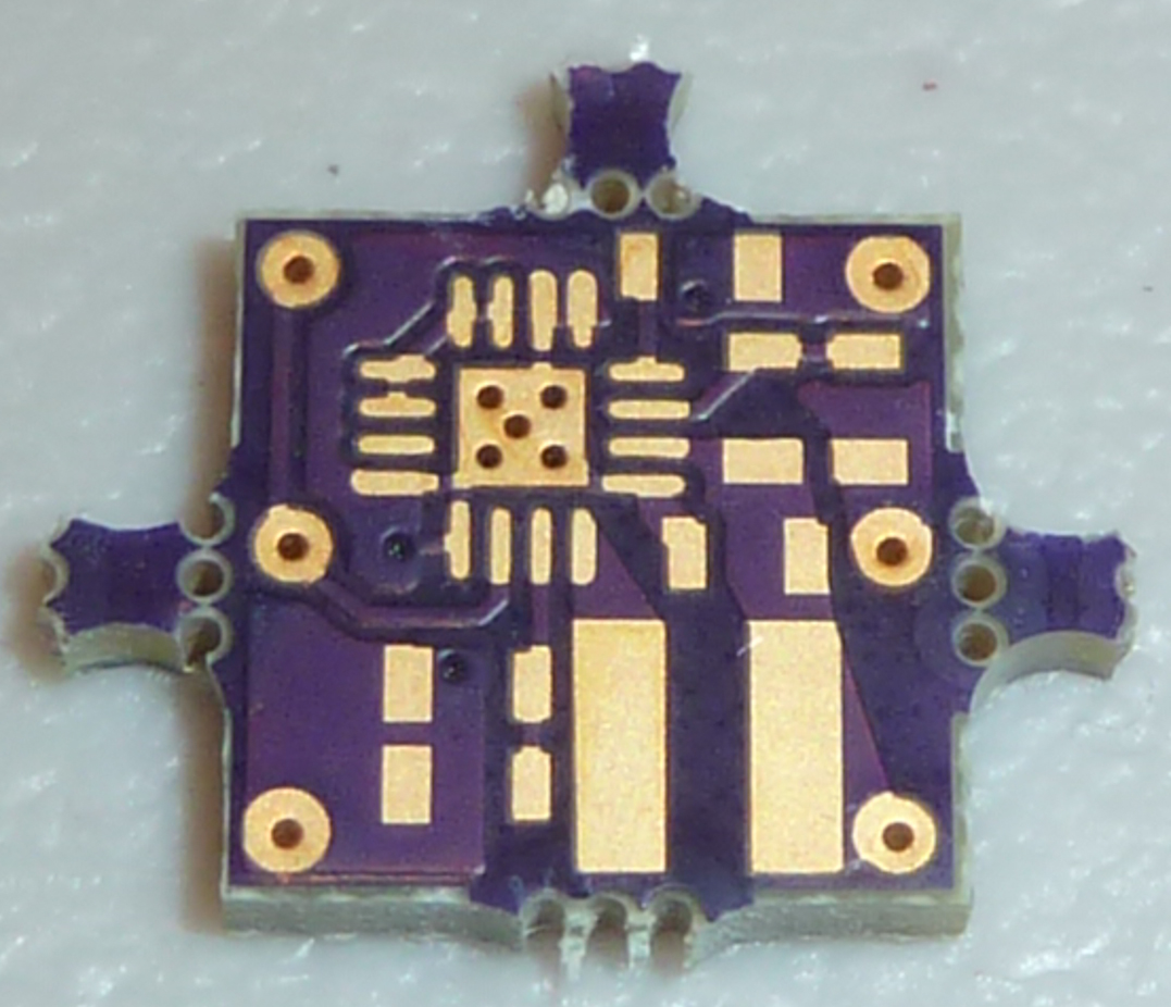
Wally is in your GND pour, in each of your board I think.
I mean you should not have any gnd around some settings resistors and capa.
Check carefully the section 11.1 Layout Guidelines in datasheet.
This is why on the reference layout you see Top GND only on half board. Or then it may happen less performance depending of mutliple factors.
It's also explained how to route the GND.That said, in case it can help, here is my gerbers https://www.dropbox.com/s/tugdbc3cfrlmdu7/bq25504_gerbers.rar?dl=0
Enjoy
-
@NeverDie said:
@scalz said:
i'm not sure, but I think i see Wally on your board ;)
LOL. You probably need better ventilation when you're soldering. The fumes are getting to you. :laughing:
:laughing: no fumes tonight, reflow oven working for me :)
Wally is in your GND pour, in each of your board I think.
I mean you should not have any gnd around some settings resistors and capa.
Check carefully the section 11.1 Layout Guidelines in datasheet.
This is why on the reference layout you see Top GND only on half board. Or then it may happen less performance depending of mutliple factors.
It's also explained how to route the GND.That said, in case it can help, here is my gerbers https://www.dropbox.com/s/tugdbc3cfrlmdu7/bq25504_gerbers.rar?dl=0
Enjoy
What is "Wally"? I haven't heard that term before, and it's not in the datasheet either. I thought you were jokingly making an obscure reference to Waldo, as in "Where's Waldo?" That's why I had thought the fumes must have gotten to you. I realize now that Wally must instead be a French electrical term of some kind.
-
@NeverDie
ahah :)If it can help you, here it is : https://oshpark.com/shared_projects/XRsFBtzu
This is because i've generated the gerbers with an other fabhouse CAM.
In mine, GML is the dimension layer if i remember right.
You can also open the gerbers in a viewer like Gerbv etc..
For oshpark, i have modified it a little bit because of slightly different DRC. -
@NeverDie
ahah :)If it can help you, here it is : https://oshpark.com/shared_projects/XRsFBtzu
This is because i've generated the gerbers with an other fabhouse CAM.
In mine, GML is the dimension layer if i remember right.
You can also open the gerbers in a viewer like Gerbv etc..
For oshpark, i have modified it a little bit because of slightly different DRC.@scalz
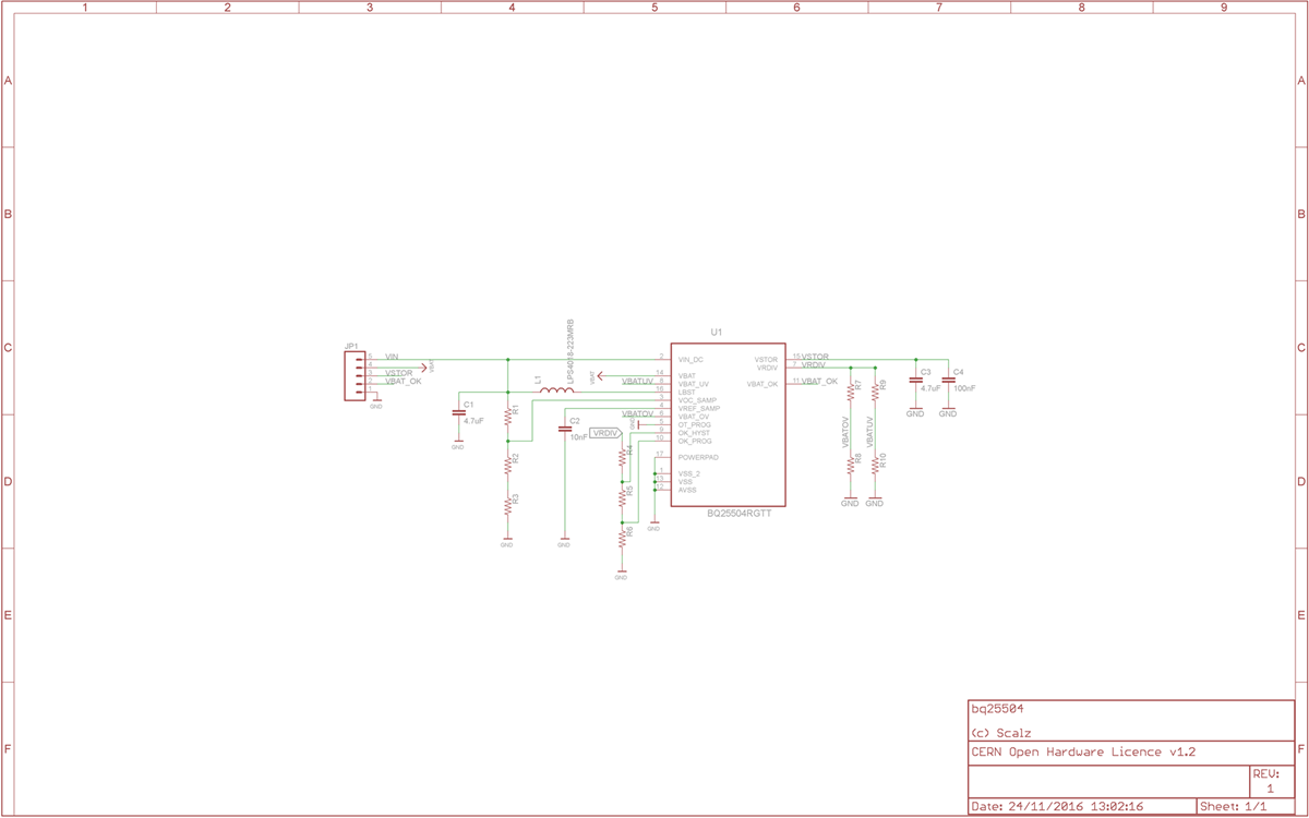
Thanks. I just now ordered it.Interestingly, if you look at Ti's eval board for the bq25504, they do in fact connect the top and bottom ground planes, and the thermal pad on the BQ25504 is connected to the entire bottom ground plane, not just another small thermal pad:
-
@NeverDie
cool.
Well, perhaps it's ok. I followed datasheet guidelines..no matter the powerpad is connected on top.Perhaps, you may need the schematic to know where parts are placed ;)
You'll need to set your resistors of course.If really needed, no problem i can upload all the files..
-
@NeverDie
cool.
Well, perhaps it's ok. I followed datasheet guidelines..no matter the powerpad is connected on top.Perhaps, you may need the schematic to know where parts are placed ;)
You'll need to set your resistors of course.If really needed, no problem i can upload all the files..
You should upload it to https://www.openhardware.io/ I'm sure a lot of people would find it very helpful.
-
@NeverDie
cool.
Well, perhaps it's ok. I followed datasheet guidelines..no matter the powerpad is connected on top.Perhaps, you may need the schematic to know where parts are placed ;)
You'll need to set your resistors of course.If really needed, no problem i can upload all the files..
-
@scalz
Out of curiosity, why did you choose such a large inductor? I notice that the "stripped" BQ25504 pcb (photo above) did the same thing. Are there advantages to the larger size?@NeverDie said:
@scalz
Out of curiosity, why did you choose such a large inductor? I notice that the "stripped" BQ25504 pcb (photo above) did the same thing. Are there advantages to the larger size?Nevermind. I see now from your schematic that you're using the coilcraft inductor from Table 1 of the DS.
-
Interestingly, looking at the Tindie board now, it's clear based on its inductor's dimensions that the Tindie board is not using one of the Table 1 recommended inductors. Perhaps that explains why the Tindie board appears to be sucking wind at the lower voltages.
-
Interestingly, looking at the Tindie board now, it's clear based on its inductor's dimensions that the Tindie board is not using one of the Table 1 recommended inductors. Perhaps that explains why the Tindie board appears to be sucking wind at the lower voltages.
@NeverDie
Coilcraft doesn't seem very available in the US, but Wurth has a similar one that's still on the DS table list that's probably a good substitute: http://www.digikey.com/product-detail/en/wurth-electronics-inc/744031220/732-1012-1-ND/1639073Also, I'll have to update my board to use a larger inductor. I had blithely assumed, based on the Tindie board, that an 0805 would be sufficient, but now that I'm digging into it probably not.
-
@NeverDie
Coilcraft doesn't seem very available in the US, but Wurth has a similar one that's still on the DS table list that's probably a good substitute: http://www.digikey.com/product-detail/en/wurth-electronics-inc/744031220/732-1012-1-ND/1639073Also, I'll have to update my board to use a larger inductor. I had blithely assumed, based on the Tindie board, that an 0805 would be sufficient, but now that I'm digging into it probably not.
@NeverDie
I take it back. The Wurth component I just referenced has a rather complex looking land pattern.Fortunately, the last remaining component on the Table 1 recommended list is a Wurth that has a much easier land pattern: http://www.digikey.com/product-detail/en/wurth-electronics-inc/744025220/732-2619-1-ND/2445718
-
@NeverDie
yep from guidelines.
but also because it's better to use shielded inductors for multiple reasons like EMI..and also good inductors and parts give better perf, efficiency etc.. lot of docs on this.That said, the footprint i use is also compatible with the 0805 advised in datasheet if i remember. it's possible to use both ref for the same footprint i've not the datasheet in front of me right now but width shoud be ok.
It seems as though TI's evaluation board ignores the design recommendations given in the datasheet, in particular: "...it is highly recommended that no ground planes be poured near the voltage setting resistors or the sample and hold capacitor." In the case of the TI's evaluation board, virtually the entire bottom layer is a ground plane. I don't know what to make of that.
Anyhow, I ordered the Wurth inductors. I also ordered a 3x3 QFN-16 solder stencil as some fallback insurance, as the BQ25504 looks like it will be very challenging to solder.
-
Also, the layout guidelines say, " It is best to use vias and bottom traces for connecting the inductor to its respective pins instead of the capacitors." Yet, the recommended layout doesn't do that.
Part of what's strange is the Recommended Layout (Figure 34 in the datasheet) shows pin 12 belonging to a different ground plane than pin 13. Yet, the schematic shows pins 12 and 13 wired directly together.
@scalz
Just where are the two different ground planes supposed to connect together? Or is one supposed to float relative to the other? -
@NeverDie
ok i'll put on my git&openhardware asap.about the planes, you're right. I've a little doubt. on most designs, it's directly to gnd. i understand about the layout guidelines. but the datasheet picture layout is a bit confusing, if it's internally connected or not..i'll check a bit later.
good point ;)
-
@NeverDie
ok i'll put on my git&openhardware asap.about the planes, you're right. I've a little doubt. on most designs, it's directly to gnd. i understand about the layout guidelines. but the datasheet picture layout is a bit confusing, if it's internally connected or not..i'll check a bit later.
good point ;)
Section 11.1 says, "When laying out the non-power ground return paths (e.g. from resistors and CREF), it is recommended to use short traces as well, separated from the power ground traces and connected to AVSS pin 12. This avoids ground shift problems, which can occur due to superimposition of power ground current and control ground current. The PowerPad should not be used as a power ground return path."
I think that's why in the Recommended Layout (Figure 34), pins 12 and 13 are not connected directly together. However, on your board, they are directly connected, probably because of the schematic.
What do they mean by "The PowerPad"? Do they mean the thermal pad beneath the chip? Maybe that's another reason why pin 12 is not connected to the thermal pad in the Recommended Layout.
I don't know what the right answer is. I'm just trying to make sense of what seem like inconsistencies in the datasheet.