Powering mote 24/7 using only a supercap and solar
-
Interestingly, looking at the Tindie board now, it's clear based on its inductor's dimensions that the Tindie board is not using one of the Table 1 recommended inductors. Perhaps that explains why the Tindie board appears to be sucking wind at the lower voltages.
-
Interestingly, looking at the Tindie board now, it's clear based on its inductor's dimensions that the Tindie board is not using one of the Table 1 recommended inductors. Perhaps that explains why the Tindie board appears to be sucking wind at the lower voltages.
@NeverDie
Coilcraft doesn't seem very available in the US, but Wurth has a similar one that's still on the DS table list that's probably a good substitute: http://www.digikey.com/product-detail/en/wurth-electronics-inc/744031220/732-1012-1-ND/1639073Also, I'll have to update my board to use a larger inductor. I had blithely assumed, based on the Tindie board, that an 0805 would be sufficient, but now that I'm digging into it probably not.
-
@NeverDie
Coilcraft doesn't seem very available in the US, but Wurth has a similar one that's still on the DS table list that's probably a good substitute: http://www.digikey.com/product-detail/en/wurth-electronics-inc/744031220/732-1012-1-ND/1639073Also, I'll have to update my board to use a larger inductor. I had blithely assumed, based on the Tindie board, that an 0805 would be sufficient, but now that I'm digging into it probably not.
@NeverDie
I take it back. The Wurth component I just referenced has a rather complex looking land pattern.Fortunately, the last remaining component on the Table 1 recommended list is a Wurth that has a much easier land pattern: http://www.digikey.com/product-detail/en/wurth-electronics-inc/744025220/732-2619-1-ND/2445718
-
@NeverDie
yep from guidelines.
but also because it's better to use shielded inductors for multiple reasons like EMI..and also good inductors and parts give better perf, efficiency etc.. lot of docs on this.That said, the footprint i use is also compatible with the 0805 advised in datasheet if i remember. it's possible to use both ref for the same footprint i've not the datasheet in front of me right now but width shoud be ok.
It seems as though TI's evaluation board ignores the design recommendations given in the datasheet, in particular: "...it is highly recommended that no ground planes be poured near the voltage setting resistors or the sample and hold capacitor." In the case of the TI's evaluation board, virtually the entire bottom layer is a ground plane. I don't know what to make of that.
Anyhow, I ordered the Wurth inductors. I also ordered a 3x3 QFN-16 solder stencil as some fallback insurance, as the BQ25504 looks like it will be very challenging to solder.
-
Also, the layout guidelines say, " It is best to use vias and bottom traces for connecting the inductor to its respective pins instead of the capacitors." Yet, the recommended layout doesn't do that.
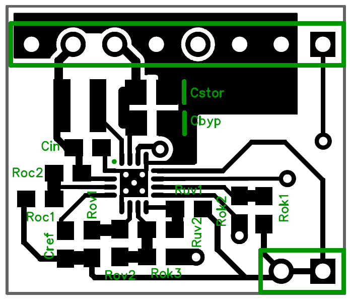
Part of what's strange is the Recommended Layout (Figure 34 in the datasheet) shows pin 12 belonging to a different ground plane than pin 13. Yet, the schematic shows pins 12 and 13 wired directly together.
@scalz
Just where are the two different ground planes supposed to connect together? Or is one supposed to float relative to the other? -
@NeverDie
ok i'll put on my git&openhardware asap.about the planes, you're right. I've a little doubt. on most designs, it's directly to gnd. i understand about the layout guidelines. but the datasheet picture layout is a bit confusing, if it's internally connected or not..i'll check a bit later.
good point ;)
-
@NeverDie
ok i'll put on my git&openhardware asap.about the planes, you're right. I've a little doubt. on most designs, it's directly to gnd. i understand about the layout guidelines. but the datasheet picture layout is a bit confusing, if it's internally connected or not..i'll check a bit later.
good point ;)
Section 11.1 says, "When laying out the non-power ground return paths (e.g. from resistors and CREF), it is recommended to use short traces as well, separated from the power ground traces and connected to AVSS pin 12. This avoids ground shift problems, which can occur due to superimposition of power ground current and control ground current. The PowerPad should not be used as a power ground return path."
I think that's why in the Recommended Layout (Figure 34), pins 12 and 13 are not connected directly together. However, on your board, they are directly connected, probably because of the schematic.
What do they mean by "The PowerPad"? Do they mean the thermal pad beneath the chip? Maybe that's another reason why pin 12 is not connected to the thermal pad in the Recommended Layout.
I don't know what the right answer is. I'm just trying to make sense of what seem like inconsistencies in the datasheet.
-
I suppose if worse came to worst, we could try answering the question empirically by using a test setup similar to this:
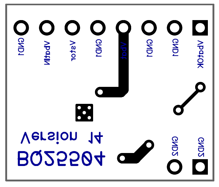
In this instance I partitioned the data ground from the power ground, and the two are not connected. However, via the header pins, a jumper could be connected between the two grounds. The experiment would be to try it both ways--connected vs. unconnected--and see which performs better.
-
The through holes on the stripped BQ25504 PCB (above)from Osh Park have too small a diameter to fit header pins into. In fact, it would require a very narrow gauge wire (narrower than what I have) to fit into it. So, unfortunately, I have doubts as to whether I will be able to test it, let alone use it.
This is all rather disappointing. :confounded: So far nothing about the BQ25504 has been easy.
-
Not that it proves anything, but using KiCAD to look at the BQstripped PCB, I notice that the PCB designer chose to connect pins 12 and 13 both directly to each other and directly to the thermal pad.
@NeverDie said:
Not that it proves anything, but using KiCAD to look at the BQstripped PCB, I notice that the PCB designer chose to connect pins 12 and 13 both directly to each other and directly to the thermal pad.
Did you say KiCAD? :+1: :+1: :+1:
-
@NeverDie said:
Not that it proves anything, but using KiCAD to look at the BQstripped PCB, I notice that the PCB designer chose to connect pins 12 and 13 both directly to each other and directly to the thermal pad.
Did you say KiCAD? :+1: :+1: :+1:
@blacey said:
Did you say KiCAD? :+1: :+1: :+1:
Yup. I had to use KiCAD to confirm the proper chip orientation before attempting to hand solder it to their PCB. Looks like a nice program.
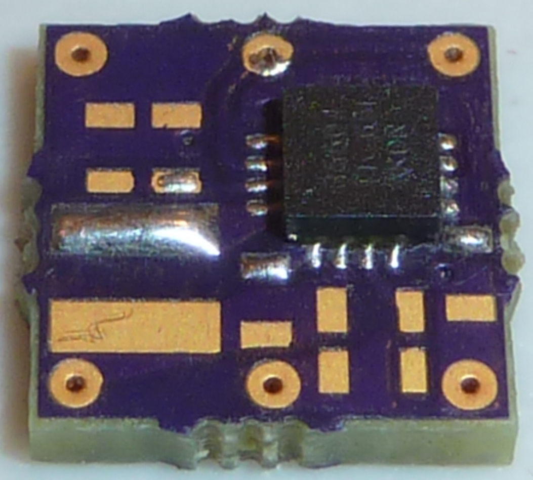
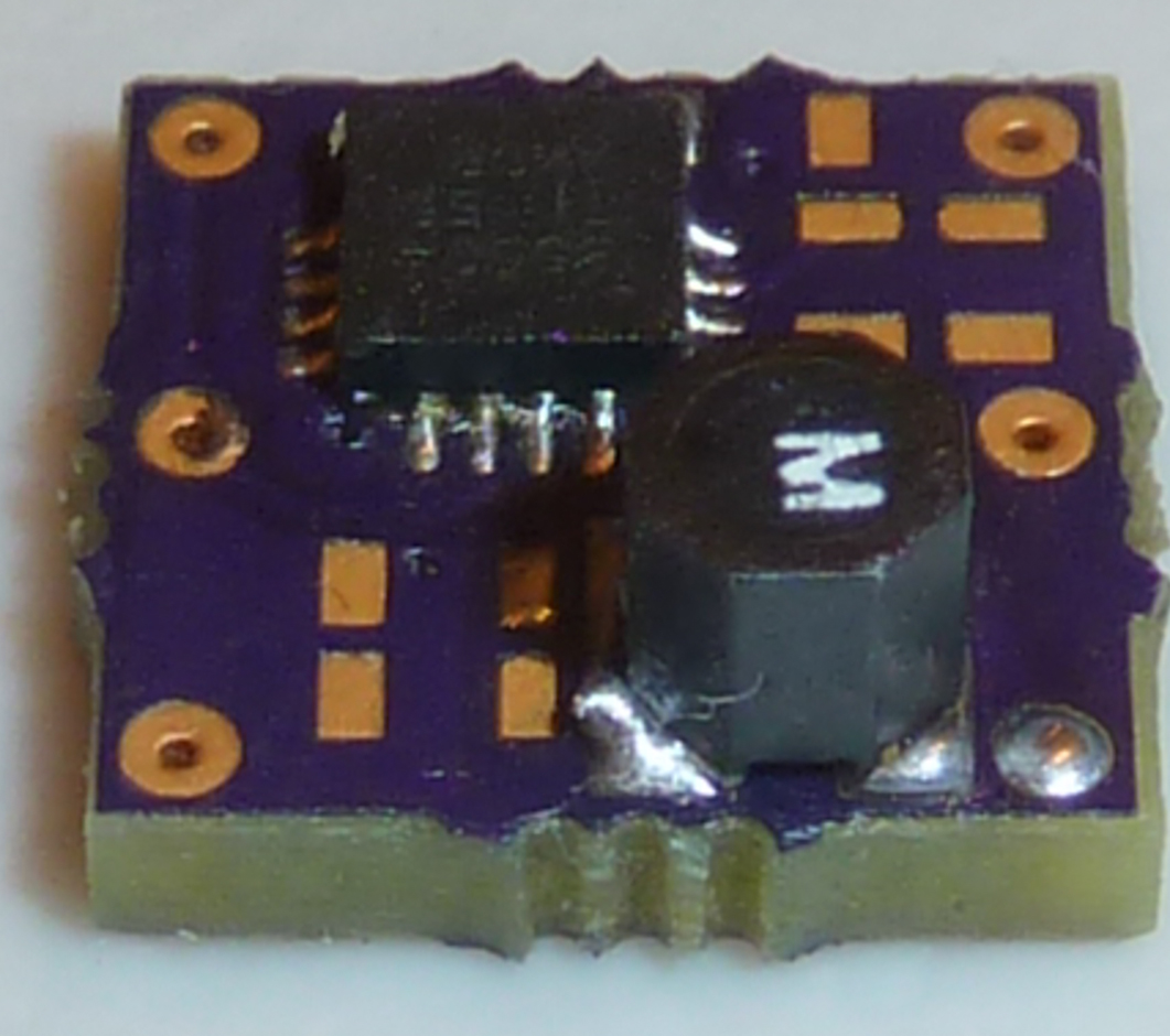
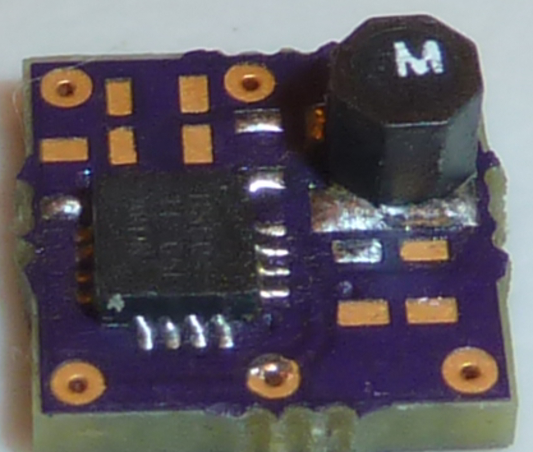
I had doubts I could hand solder the BQ25504, but I tried it using Dave Jones's tack and reflow method, and to my untrained eye it looks like it came out OK, despite the chip not being completely well aligned with the solder pads:
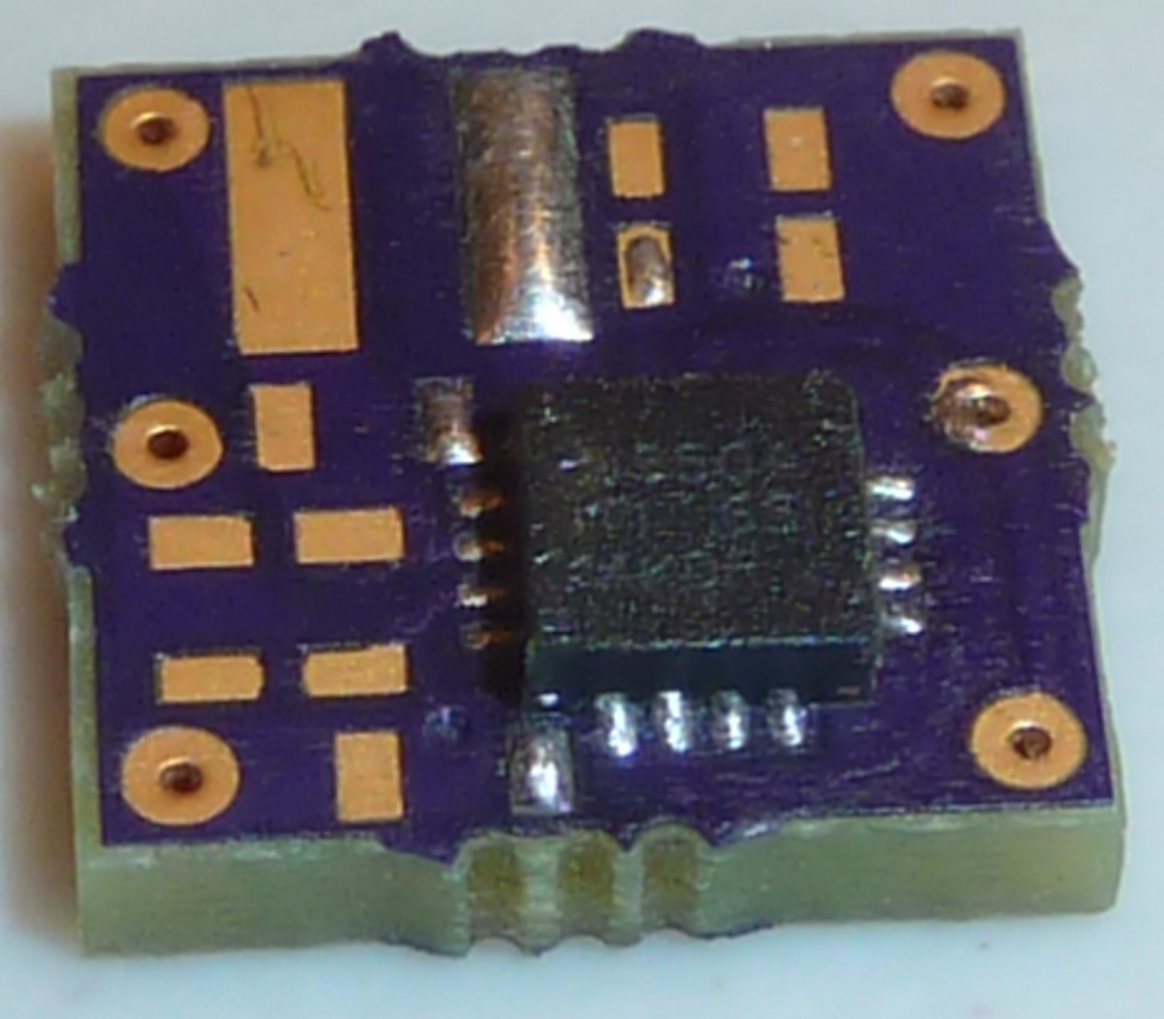
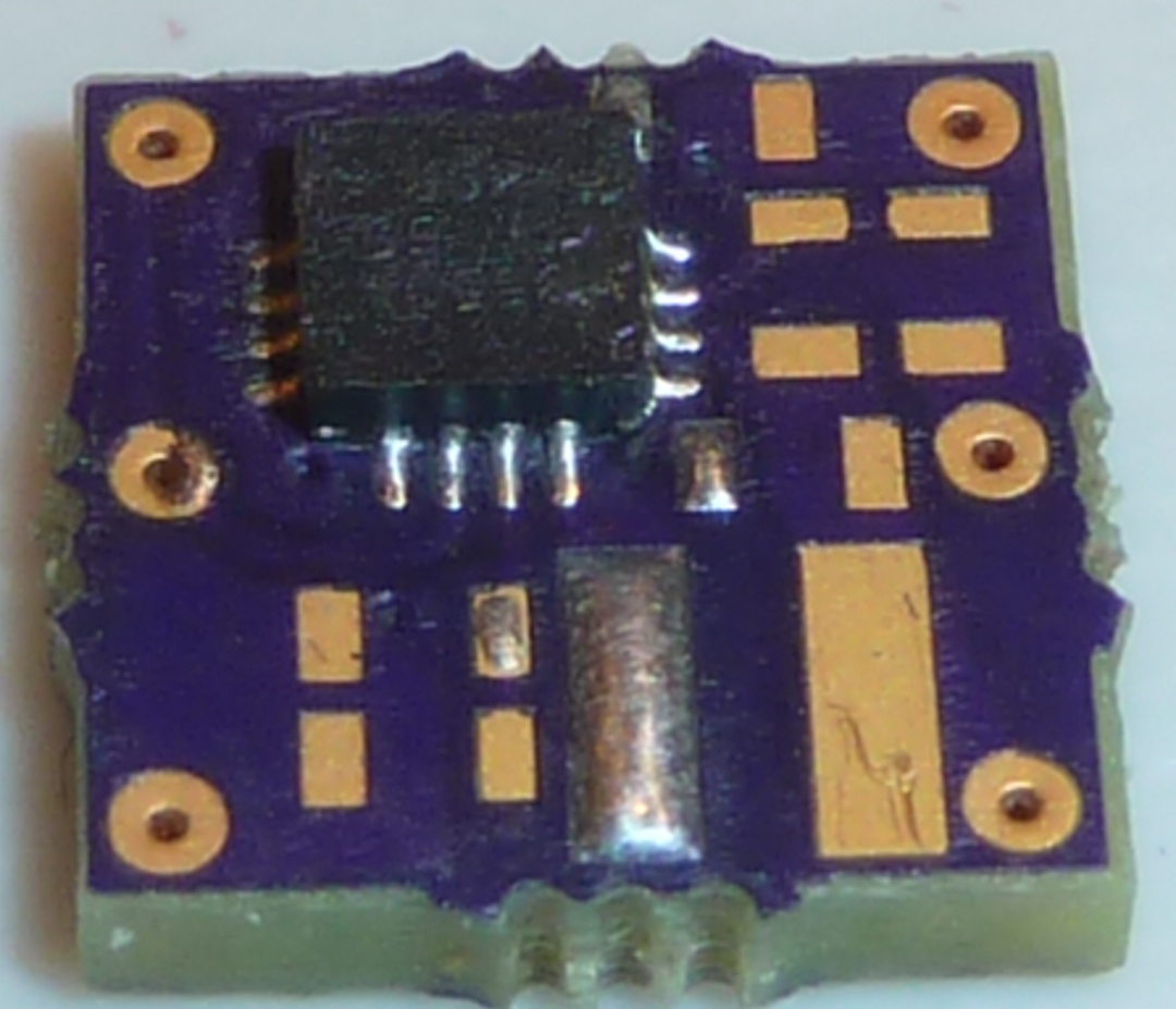
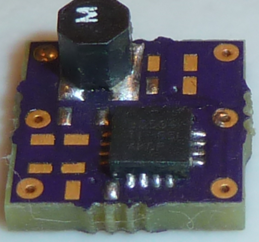
The Wurth inductors arrived today, so I'll have a go at soldering that on next. Hopefully the BQstripped PCB designer picked the same one I did!
-
Looks as though the inductor hand soldered as well:
-
Interestingly, if one looks at the KiCad schematic for the bqstripped PCB, you will notice that it draws a distinction between regular GND and GNDPWR:
0_1480428663373_kicad_schematic.pdfHowever, as already noted, that distinction seems to be cast aside when they laid out the PCB traces, since pins 12 and 13 are connected together directly by a trace. Indeed, the schematic explicitly shows GNDPWR connected to GND. So, why create the distinction in the first place?
-
@NeverDie
this is for the power gnd plane regarding the analog gnd plane. analog for instance should be connected at one point. but then in practice like you said it looks a bit different...
don't worry too much i think!
The good in this, is i think, you have learnt good things (taking care of datasheet guidelines etc...) for future :thumbsup: -
I had to order some 4.7uF smd 0603 capacitors and 4.42M ohm 0603 resistors.
The DS also calls for 15.62M ohm resistors, but the closest thing that Digikey carries is 15M ohm 0603 smd's, so that's what I ordered.
Meanwhile I did solder the 10nf capacitors to the BQstripped pcb, as I had those on hand. If I had it to do over, I would probably have soldered them prior to soldering the BQ25504 and the 22uH inductor, as those parts were in the way.
-
I had to order some 4.7uF smd 0603 capacitors and 4.42M ohm 0603 resistors.
The DS also calls for 15.62M ohm resistors, but the closest thing that Digikey carries is 15M ohm 0603 smd's, so that's what I ordered.
Meanwhile I did solder the 10nf capacitors to the BQstripped pcb, as I had those on hand. If I had it to do over, I would probably have soldered them prior to soldering the BQ25504 and the 22uH inductor, as those parts were in the way.
Just a few notes on a conservative approach to component selection for boost converters that I've lately gleaned from reading various datasheets:
-
Ideally, capacitors should be rated X5R or X7R.
-
For inductors, generally speaking the lower the DCR the better, provided that the saturation current remains appropriately high enough. For instance, the B82462G4 series (http://www.digikey.com/product-search/en/inductors-coils-chokes/fixed-inductors/196627?k= +B82462G4&k=&pkeyword= +B82462G4&pv7=2&mnonly=0&newproducts=0&ColumnSort=0&page=1&quantity=0&ptm=0&fid=0&pageSize=500 ) has much lower DCR than any of the datasheet recommended inductors. These inductors are more expensive, but their use should, in theory, lead to higher efficiency and/or lower start/operating voltages. Also, I suspect the Tindie board's performance is impaired by its choice of inductor, because I haven't seen specs on any inductors as small as theirs is that has a low DCR.
-