CNC PCB milling
-
@andrew said in CNC PCB milling:
could you please explain how did you find/measure this?
- Decided upon an origen. Used Chilipeppr to "run test probe" to find the zero z-height. Zeroed x,y,z at that location.
- Did an autolevel, at 1mm spacing, over a 20x10mm area.
- Following this, returned to x=0, y=0. Ran another test probe. Ideally it would have come back as z=0. Instead, it came back as z=-0.048.
So, if at that point I were to actually run g-code with a cutting depth of z=-0.05, it would barely scratch the surface. Somehow during the 1mm autolevel probing, z became uncalibrated. If I were to re-zero z based on the second test probe, it would cut, but the cutting depth wouldn't be uniform.
Anyhow, my new rule is that if I come across a situation like the above, I throw out the auto-leveling and start over rather than executing the g-code. Often, the next autoleveling will have less discrepancy by step 3.
@neverdie said in CNC PCB milling:
@andrew said in CNC PCB milling:
could you please explain how did you find/measure this?
- Decided upon an origen. Used Chilipeppr to "run test probe" to find the zero z-height. Zeroed x,y,z at that location.
- Did an autolevel, at 1mm spacing, over a 20x10mm area.
- Following this, returned to x=0, y=0. Ran another test probe. Ideally it would have come back as z=0. Instead, it came back as z=-0.048.
So, if at that point I were to actually run g-code with a cutting depth of z=-0.05, it would barely scratch the surface. Somehow during the 1mm autolevel probing, z became uncalibrated. If I were to re-zero z based on the second test probe, it would cut, but the cutting depth wouldn't be uniform.
Anyhow, my new rule is that if I come across a situation like the above, I throw out the auto-leveling and start over rather than executing the g-code. Often, the next autoleveling will have less discrepancy by step 3.
if your probe speed is too fast, then it could push the pcb at the given points and also it could damage your tip's end, as it was mentioned by @rmtucker, which could cause this issue as well.
-
@andrew said in CNC PCB milling:
did you manage to create double sided PCB jobs in the meantime based on my suggestion and on flatcam's documentation? it is not a hardcore process, let me know if you stuck at a given step.
Not sure what kind of pins to use for the alignment.
@neverdie said in CNC PCB milling:
@andrew said in CNC PCB milling:
did you manage to create double sided PCB jobs in the meantime based on my suggestion and on flatcam's documentation? it is not a hardcore process, let me know if you stuck at a given step.
Not sure what kind of pins to use for the alignment.
I missed this reply from you.
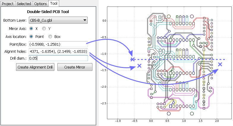
so, you have to define the alignment holes, typically outside of the actual pcb area, in the "frame".
you have to define two of them, the rest will be calculated automatically.the steps are exactly the same as that you can see on http://flatcam.org/manual/procedures.html#side-pcb
see the pic below. note, that you don't have to write the coordinates to the input boxes manually, once you click on the design area the corresponding coordinates will be copied to the clipboard, so you can use ctrl-v to fill out the settings.
- click on the picture to define the axis (X in this example)
- copy the corresponding coordinates to the point/box input filed
- click on the design area to define the exact location of the first alignment hole (left side of the actual pcb)
- copy the corresponding coordinates to the alignment holes input filed
- click on the design area to define the exact location of the first alignment hole (right side of the actual pcb)
- copy the corresponding coordinates to the alignment holes input filed. the two set of coordinates have to be separated by coma.
- configure the alignment holes' drill size
- click on the create align drill button and you're done. back on the project tab you can find a new drill job which you have to further process to create the belonging G code from it.
-
@neverdie said in CNC PCB milling:
@andrew said in CNC PCB milling:
did you manage to create double sided PCB jobs in the meantime based on my suggestion and on flatcam's documentation? it is not a hardcore process, let me know if you stuck at a given step.
Not sure what kind of pins to use for the alignment.
I missed this reply from you.
so, you have to define the alignment holes, typically outside of the actual pcb area, in the "frame".
you have to define two of them, the rest will be calculated automatically.the steps are exactly the same as that you can see on http://flatcam.org/manual/procedures.html#side-pcb
see the pic below. note, that you don't have to write the coordinates to the input boxes manually, once you click on the design area the corresponding coordinates will be copied to the clipboard, so you can use ctrl-v to fill out the settings.
- click on the picture to define the axis (X in this example)
- copy the corresponding coordinates to the point/box input filed
- click on the design area to define the exact location of the first alignment hole (left side of the actual pcb)
- copy the corresponding coordinates to the alignment holes input filed
- click on the design area to define the exact location of the first alignment hole (right side of the actual pcb)
- copy the corresponding coordinates to the alignment holes input filed. the two set of coordinates have to be separated by coma.
- configure the alignment holes' drill size
- click on the create align drill button and you're done. back on the project tab you can find a new drill job which you have to further process to create the belonging G code from it.
-
@andrew Are you using male header pins for your alignment? How deep are you drilling the holes them?
-
@neverdie yes, I use male pins, with 0.7mm drill (so it is tight for the pin), 5mm depth. but this is really up to you, choose anything which you have easy access to.
With single sided PCB, I soldered the ground wire (for probing) to the copper cladding, just as the Chilipeppr author did. How are you handling it for two sided? If I do it that way for two sided, the solder bump may prevent the board laying flat on the wasteboard.
-
With single sided PCB, I soldered the ground wire (for probing) to the copper cladding, just as the Chilipeppr author did. How are you handling it for two sided? If I do it that way for two sided, the solder bump may prevent the board laying flat on the wasteboard.
@neverdie I use a wood screw in the sacrificial board holding a piece of metal as a "clamp" I slide it over the board (1mm overlap) and clip one alligator clip to the screw, the other to the bit. After probing I slide it out of the way. The metal piece is about 10cm long and it's left in place for the life of the wood board.
-
With single sided PCB, I soldered the ground wire (for probing) to the copper cladding, just as the Chilipeppr author did. How are you handling it for two sided? If I do it that way for two sided, the solder bump may prevent the board laying flat on the wasteboard.
@neverdie said in CNC PCB milling:
With single sided PCB, I soldered the ground wire (for probing) to the copper cladding, just as the Chilipeppr author did. How are you handling it for two sided? If I do it that way for two sided, the solder bump may prevent the board laying flat on the wasteboard.
I use some flat metal weight connected to the given wire, placed on top of the pcb.
-
hackaday just released a relevant post:
https://hackaday.com/2018/01/04/guide-why-etch-when-you-can-mill/@andrew said in CNC PCB milling:
hackaday just released a relevant post:
https://hackaday.com/2018/01/04/guide-why-etch-when-you-can-mill/Interesting that the engraving bits he liked the best were the 30 degree 0.1mm bits. So far, that's been my preference as well.
-
@andrew said in CNC PCB milling:
hackaday just released a relevant post:
https://hackaday.com/2018/01/04/guide-why-etch-when-you-can-mill/Interesting that the engraving bits he liked the best were the 30 degree 0.1mm bits. So far, that's been my preference as well.
-
@yveaux said in CNC PCB milling:
@neverdie Possibly too late, but it still might contain some handy tips: https://hackaday.com/2018/01/04/guide-why-etch-when-you-can-mill
It nicely sums up the biggest challenge of all:
The biggest challenge in this DIY process is getting a correct and consistent cutting depth. These V-bits yield a wider cut the deeper you go, effectively robbing you of precious engraving resolution. If you do not tune in just the right depth, some traces will come out too thin and frail.
The results I'm getting seem random. Sometimes it's great. Sometimes it's totally unusable (obliterated traces). Some of the time it's usable, but only just barely.
So, I'm trying to think of a better approach that might deal with that. Maybe one way might be to start every etching session by running @executivul 's calibration traces. If it's cutting too deep, adjust, and then run again. When it's finally cutting right, then cut the desired PCB traces.
I don't know what the answer is, but that's where it currently stands with me.
The alternative is to just make a number of boards. Then cherry pick the good ones and dispose of the rest.
-
I think I've found at least one reason for the trouble I've been having: sometimes the double sided scotch tape hasn't been holding the board completely flat against the waste board. Instead, during the milling process, which has a lot of vibration, it can pop up in the area being milled. When that happens, it's effectively the same as having the milling go much deeper, and so traces can be obliterated. Hence, I may try the Shurtape GG-200 that was recommended in the Hackaday article.
It may be that the copper clad boards I'm using just aren't flat enough in the first place. Add to that a waste board that may not be perfectly flat either, and it's not a good formula for keeping everything perfectly flat, which is evidently what it needs to be. The tape itself can't compensate for too large a mismatch.
So, I'd like to try the earlier idea of milling the waste board flat. Just not sure how to do that.
I would't be surprised if single sided copper clad boards are inherently prone to warping. If you think about it, the copper can expand/contract with temperature, and if it's on only one side....Unless the substrate has the same coefficient of thermal expansion, the result will inevitably be warping. The same would be true if the substrate is affected by humidity.
The Hackaday article does mention that it's not necessarily easy to find good copper clad boards. He hints that it has been an ongoing issue over time. He gives a reference for an ebay board vendor in England that he currently likes, but unfortunately that doesn't help me much.
What blank copper clad boards have folks here found that they like?
@neverdie Perhaps surface cleanliness is the problem rather than the tape, just a possibility... When you are dealing with such fine tolerances, any residue will allow the board to twist or warp...
Not sure to what extent the milling itself would encourage deformation of the substrate, but irrespective, it would again depend on adhesion on the bottom face to resist it... -
@neverdie Perhaps surface cleanliness is the problem rather than the tape, just a possibility... When you are dealing with such fine tolerances, any residue will allow the board to twist or warp...
Not sure to what extent the milling itself would encourage deformation of the substrate, but irrespective, it would again depend on adhesion on the bottom face to resist it...@zboblamont said in CNC PCB milling:
@neverdie Perhaps surface cleanliness is the problem rather than the tape, just a possibility... When you are dealing with such fine tolerances, any residue will allow the board to twist or warp...
Not sure to what extent the milling itself would encourage deformation of the substrate, but irrespective, it would again depend on adhesion on the bottom face to resist it...You raise a good point. I suppose ideally the waste board would be covered in melamine or similar so that it can be cleaned of any bond breakers.
-
@zboblamont said in CNC PCB milling:
@neverdie Perhaps surface cleanliness is the problem rather than the tape, just a possibility... When you are dealing with such fine tolerances, any residue will allow the board to twist or warp...
Not sure to what extent the milling itself would encourage deformation of the substrate, but irrespective, it would again depend on adhesion on the bottom face to resist it...You raise a good point. I suppose ideally the waste board would be covered in melamine or similar so that it can be cleaned of any bond breakers.
@neverdie Not sure whether you mean a slab of melamine or a laminated board...
I'm sure I saw a video clip where a perspex or similar baseplate was mounted on the bedplate to provide a perfectly flat surface. The user released the adhesive tape using wd40 or similar, then cleaned the area afterward with alcohol.
If I remember correctly, the perspex had locating dowels for the PCB, and always locked into specific location on the frame. If I find the video again will link it... -
@neverdie Not sure whether you mean a slab of melamine or a laminated board...
I'm sure I saw a video clip where a perspex or similar baseplate was mounted on the bedplate to provide a perfectly flat surface. The user released the adhesive tape using wd40 or similar, then cleaned the area afterward with alcohol.
If I remember correctly, the perspex had locating dowels for the PCB, and always locked into specific location on the frame. If I find the video again will link it...@zboblamont said in CNC PCB milling:
Not sure whether you mean a slab of melamine or a laminated board...
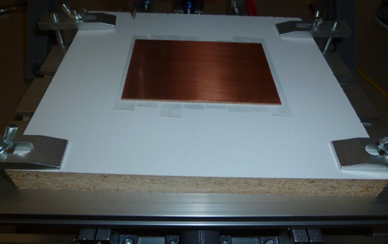
Just laminated. Here, I've already made the switch:
-
I've seen people engrave round objects based only on autoleveling, gcode was generated for a flat surface. So autolevel should take care of the board not being perfectly flat. Only issue is to chose a grid step small enough so the matrix can follow the hills and valleys (3-5mm).
On the other hand autolevel can not compensate for the board moving. Probing force is much lower than milling force. So when milling pcb prefers to move down and you get a shallow engrave where it was probed higher due to being lose.
Lost steps should add, so a constantly deeper and deeper or shallower and shallower engrave would make me think of lost steps.
I would try changing the probing speed to 10-15 and z max feedrate to 50, z max accel to 10. Add some grease to z axis components (engine/transmission oil or very light grease), a few drops goes a long way.
Also make sure you do the z zeroing at 0,0 and don't reprobe at another point after the grid probing.LE. Rail bowing under gantry weight is another problem, it would appear as a convex (inverted soup bowl) surface, since in the middle of the rail the gantry goes lower so the surface appears to be higher.
A dial gauge with a magnetic arm can be had cheaply these days and is a miracle for testing backlash and baseboard flatness. Fix the mag base to the spindle and start moving it back and forth
Even removing the moving bed and testing against the y rails might yeld some surprise.LE2: baseboard/sacrificial layer flatening works only for plastic and mdf, normal wood or big piece wood conglomerate leaves a much worse surface than the original board.
@NeverDie hope I gave you some ideas to play with, by the way I asked you earlier to do some tests for z axis repeatability, did you manage to do them?
LE3. God damn it! Now I must haz this https://m.ebay.co.uk/itm/EU-UK-3-Set-2N-m-Nema23-76mm-Hybrid-Closed-Loop-Servo-Motor-3A-HSS57-Driver-CNC/152848151184?_mwBanner=1 and all my problems should be gone!
-
@zboblamont said in CNC PCB milling:
Not sure whether you mean a slab of melamine or a laminated board...
Just laminated. Here, I've already made the switch:
@neverdie As good as any I guess if it's new board...
Curiously watched some videos, one using a smaller machine where the board was only locked from horizontal movement with pins (no tape under at all), another where MDF had been rebated to lock in a specific board size and taped down.
In the first case he only set the z-axis in the centre of the board (and a neat way of doing it too by loosening the chuck and dropping the bit then retightening once close to the stop), no surface mapping nothing. The pins were to allow double sided cutting... -
Tried the new laminated wasteboard, and so far so good:
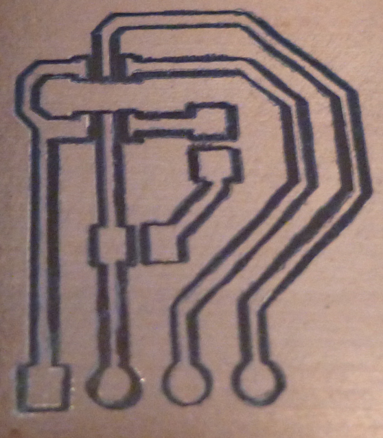
I got the above result by a method you guys are probably going to hate, but it worked. Namely, I ""sneaked up on" the correct z-depth rather than committing to a single pass at, say, z=-0.05. So, to get the above I first did a pass with z=-0.02. That did manage to cut through in some areas, but not others. So, I increased the cut to z=-0.04 and did a second pass. The result is what you see above. No need to go further to z=-0.05.Also, I did the probing (at 4mm) with a blunt used etching bit. Afterward, I switched to a new Model 20 bit, did a test probe to zero it, and then initiated the first pass.
-
So far this new approach seems to be working. Here I probed every 1mm using a blunt bit before switching to a model 10 to do the cutting at depth z=-0.03 (which was the third pass):
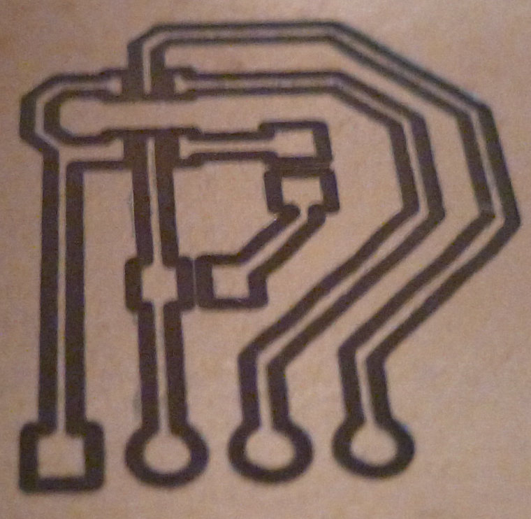
The first two passes were at z=-0.01 and z=-0.02 respectively.