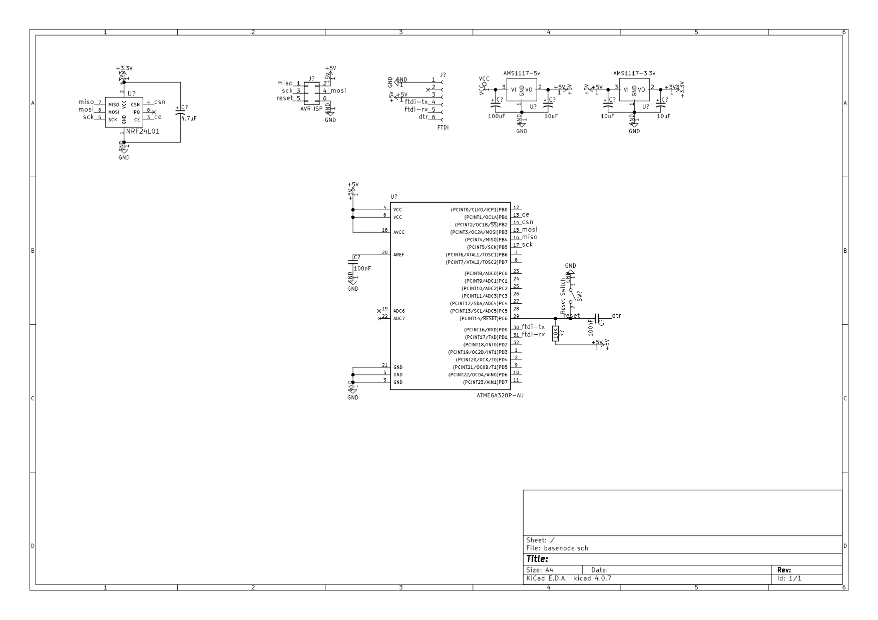
Basenode schematic.
-
Hey Guys (and girls),
I am in the process of designing PCB's for my sensors. The idea is to learn more about smd hardware hacking while designing a base node for my sensor projects.
I've drawn a schematic for the bare minimum of this node (I will add atsha/flash etc later). Are there any suggestions for my schematic? Will this work as a barebone arduino with nrf24l01?

Please advice.
Kind regards,
ByteLock -
Hi,
I'm still rather new at this myself, but here are a few questions/remarks:- How did you label your connections? I would think you need "global labels" which are surrounded by an arrow like shape in KiCad. Yours look like regular text.
- Why add +5V and +3.3V labels to your power inputs? They are globally accessible without additional labeling.
- AMS1117-3.3v datasheet mentions a single tantalum capacitor of 22uF on output only. I'm unsure why you put the other capacitors on those regulators. I used the same regulator and went by the discussion here.
- You should run the annotation tool and electronic rules check. It will probably complain about the power not being driven. You can solve this by connecting the input power and ground with the PWR_FLAG power symbol.
- You should mark the unused connections on the MCU with "no connect" cross mark.
I hope this helps.
Hello! It looks like you're interested in this conversation, but you don't have an account yet.
Getting fed up of having to scroll through the same posts each visit? When you register for an account, you'll always come back to exactly where you were before, and choose to be notified of new replies (either via email, or push notification). You'll also be able to save bookmarks and upvote posts to show your appreciation to other community members.
With your input, this post could be even better 💗
Register Login