CNC PCB milling
-
Results look much better this time:
Using Chilipeppr, I probed every 3mm and then let it rip. As before, it was cutting at z=-0.1 and a feedrate of 76.2 (the feedrate wasn't a conscience choice but rather just what flatcam gave me, for whatever reason).The good news is that it doesn't have the blatantly obvious trace obliteration that it had the first time. All in all, it looks like a definite improvement. :)
@neverdie Seems like it's getting better, still some traces in the middle are hairthin, maybe increasing tool size in flatcam a tad? like 0.12mm so it lets the tracks be wider. Bare in mind this is a prototyping machine, I use mine for low batch home automation boards, under 20 boards of the same kind, at the price of a blank pcb I can buy 10 for the price of one fab made 100x150mm, not to speak of wait time.
After you are satisfied with the board is time to get some plumber's paste for soldering copper pipes, that is used for tinning, or maybe you can find some liquid tinning solution, but that's more expensive here, I use the paste.
Then some soldermask and some uv led strips to make an exposure unit and there you have your own pcb fab at home :sunglasses:
-
@neverdie Seems like it's getting better, still some traces in the middle are hairthin, maybe increasing tool size in flatcam a tad? like 0.12mm so it lets the tracks be wider. Bare in mind this is a prototyping machine, I use mine for low batch home automation boards, under 20 boards of the same kind, at the price of a blank pcb I can buy 10 for the price of one fab made 100x150mm, not to speak of wait time.
After you are satisfied with the board is time to get some plumber's paste for soldering copper pipes, that is used for tinning, or maybe you can find some liquid tinning solution, but that's more expensive here, I use the paste.
Then some soldermask and some uv led strips to make an exposure unit and there you have your own pcb fab at home :sunglasses:
@executivul How much overlap in flatcam are you using? I've been using zero. Would changing it to something non-zero help, or is it irrelevant?
-
@executivul How much overlap in flatcam are you using? I've been using zero. Would changing it to something non-zero help, or is it irrelevant?
@neverdie I never do multiple passes, so overlap is irrelevant to me...
-
When I probe at 2mm, it often randomly fails with messages like this:
Moving to {x:12,y:28}
probe failed, clear controller alarm before resuming
Paused
Working on probe for {x:12,y:26} Found lowest Z:0.17499999999999996
Paused
What is causing these "probe failed" to happen? And how exactly am I supposed to "clear controller alarm"? It always seems that I need to disconnect from the serial port and then reconnect to get any further movement. But if I do that, it clears the x,y,z positions, effectively preventing any kind of sensible resumption. :(
-
Argh, it just happened again. This time when doing 3mm probing.
Moving to {x:12,y:27}
probe failed, clear controller alarm before resuming
Paused
Working on probe for {x:12,y:24} Found lowest Z:0.23000000000000004
Paused
How does it even decide that a probe error has happened?
-
Argh, it just happened again. This time when doing 3mm probing.
Moving to {x:12,y:27}
probe failed, clear controller alarm before resuming
Paused
Working on probe for {x:12,y:24} Found lowest Z:0.23000000000000004
Paused
How does it even decide that a probe error has happened?
@neverdie timing racing condition is f*king spjs, ugly hack is to try to increase probing starting height from 0.5mm to 1.0mm
-
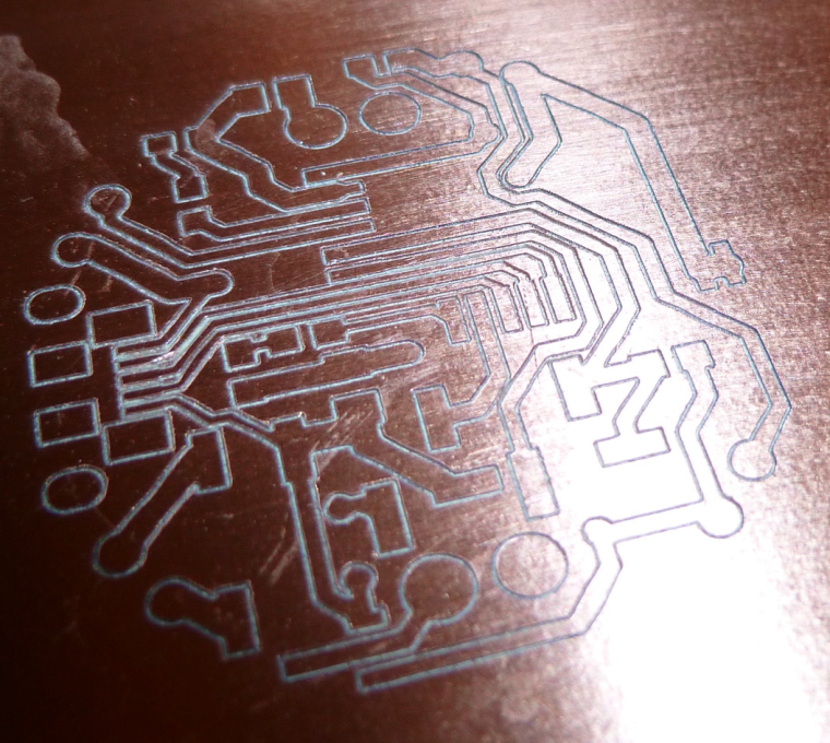
It's hard to photograph these etchings. They actually look better by eye. I tested out the last one with a continuity meter, and it seems that it would be functional (in the sense that the traces were isolated from what they should be and they connected the pads that they should.
However, without the solder mask, I'm doubtful those closely packed micro-usb pads on the middle left near the edge would be solderable without bridging.
I really hadn't considered I would ever need to do solder mask, I guess because the demo boards I've seen other people make don't seem to have it.
So, maybe a better question is: what is the minimum isolation width so that I won't need solder mask? Perhaps that becomes the limit for prototyping.
Anyhow, I'll look into it, but I really hadn't planned on taking that extra step.
-
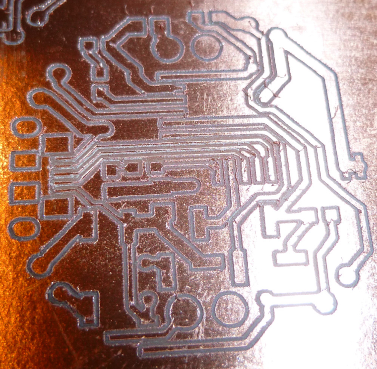
They keep getting better!
I used a fresh Jack bit to get this one. The tip on the bit used in the previous etching was a bit worn down, which I think explains the undesirable width of its cuts. I also dropped the feedrate to 50mm/minute, which may have helped also. Anyhow, most of the cuts seem very crisp compared to earlier attempts. As before, I split the line segments into 1mm lengths using the OpenCNCPilot. I think that is probably helping a lot.I did this one is two passes. The first pass was z=-0.05, and it didn't cut through enough of the copper. The second pass was z=-0.1, which is what you see above. Yet, some of the traces on the micro-usb on the middle left still don't seem fully isolated, so I'm about to try a third pass at z=-0.15
Also, this was the first job I ran with autoleveling set at 2mm. Perhaps that helped also.
-
I received my end-mill bits for cutting the PCB loose from the rest of the copper clad blank. Which got me thinking: since I have doubled sided tape on the back of the PCB blank, I presumably don't need mouse bites or similar, right? I should be able to just cut the board outline by cutting through to the sacrificial board underneath, right? Is that what others here are doing? Or are you milling tiny little supports that you break away at the end?
Regardless, what diameter end mill bit should I use for the task? What cutting depth? I'll look back to see if it's in @andrew 's list of magic numbers, but anyone else feel free to post what you like to use and do.
-
Here's what @andrew had to say:
edge cut or hole milling with the 0.8mm endmill:

feed rate: 170
z cut: -1.7mm
multi depth, depth/pass: 0.2mm
So, I guess by "z cut: -1.7mm", he likely meant that as a Z that's -1.7mm below the depth of the PCB? I'm not sure how else to interpret that.Hmmm.. I think he assumed the board thickness of 1.5mm, so he gave is 0.2mm more than that. Mine (being single sided) is 1.35mm, so I'll set cutting depth to 1.6mm, just to be sure.Aside from that, 0.8mm end mill and multiple passes at a feed rate of 170. So, I guess I use flatcam to produce the gcode that conforms to this and then run it in Chilipeppr.
And, it looks like flatcam adds the cut-out supports automatically. Nice.
-
Argh. Another probe failure:
Moving to {x:4.430000007152557,y:19.430000007152557}
probe failed, clear controller alarm before resuming
Paused
Working on probe for {x:4.430000007152557,y:24.430000007152557} Found lowest Z:0.051000000000000156
Paused
even though I have it set to start probing at z=1.0mm. This really needs to be fixed.
-
Unfortunately, I botched the third etching pass. My fault. But I decided to try the board cutout anyway:
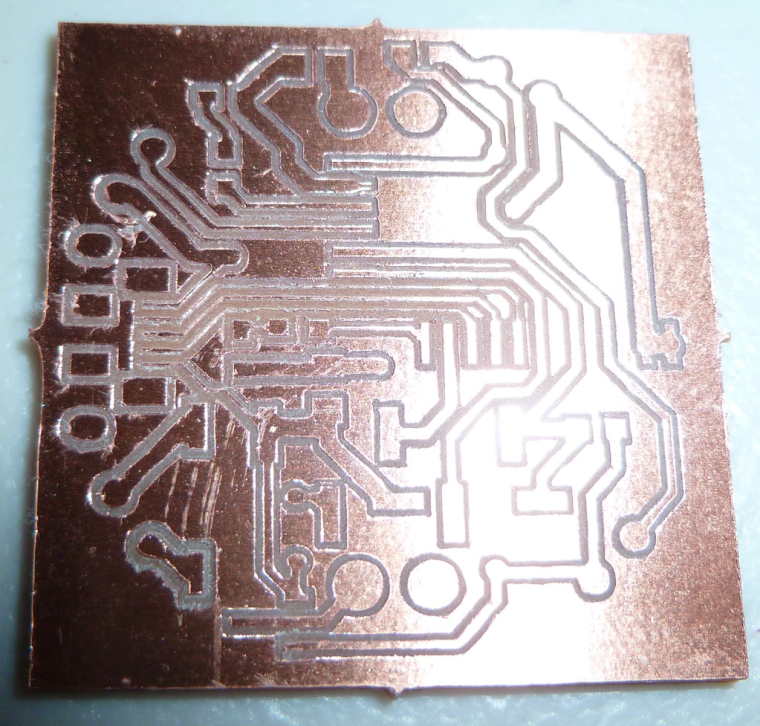
I didn't see a way for flatcam to do a circular cut-out, so I just went with the rectangular cut-out. Anyhow, it worked.
I receive my CNC drill bits on Friday, so after that I should be able to do a complete PCB of some kind. :)
-
Argh. Another probe failure:
Moving to {x:4.430000007152557,y:19.430000007152557}
probe failed, clear controller alarm before resuming
Paused
Working on probe for {x:4.430000007152557,y:24.430000007152557} Found lowest Z:0.051000000000000156
Paused
even though I have it set to start probing at z=1.0mm. This really needs to be fixed.
@neverdie said in CNC PCB milling:
This really needs to be fixed.
I wonder whether increasing the priority of the tasks using the Windows task manager might help at all? Perhaps some background tasks are interfering and slowing things down to the point where cp can't keep up with real-time?
-
@neverdie said in CNC PCB milling:
This really needs to be fixed.
I wonder whether increasing the priority of the tasks using the Windows task manager might help at all? Perhaps some background tasks are interfering and slowing things down to the point where cp can't keep up with real-time?
@neverdie there is a tutorial for custom board cutout in flatcam, "google it baby", it involves manually using open_gerber and follow commands. I'm on the phone and can't find it right now.
Regarding cutout I sugest you use 0.5mm depth and 100-150mm/min with 0.8mm endmill. Your spindle is pretty low rpm. I use 1mm depth and 300-400mm/min, 2 passes, 1.6mm thick pcb, about 40k rpm. -
For those who are interested, this is the best solder mask tutorial I was able to find:
https://www.youtube.com/watch?v=B0Syj4awcc8It doesn't look too bad, but I'd still rather not go there if I can avoid it.
However, this process doesn't seem optimized for people who are doing, say, .1mm etchings around their pads. I mean, couldn't one squeegee in the solder mask, uv cure it, and then remove what trace amounts might remain on the pads themselves by burnishing it off with a scotchbrite pad or something? I mean, for quick and dirty results that work well enough for prototyping, that's what I'd have in mind. Anyone try something like that?
The techniques on youtube for using solder mask goop aren't optimized for people who have veritable canals around their solder pads. Why not take advantage of that?
-
@NeverDie oh, you've a lot of stuff and update since my last visit here. I've just a couple of minutes now, so I just quickly checked the new posts. let me give some further details/tips to you based on the issues I see:
- flatcam does support hole milling. when you select the given drl file (project tab) you can select all of the given holes (selected tab) which you want to mill, then scroll down (see screenshot below) where you can generate the hole milling geometry.
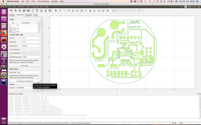
- you can find my edge cutting related details/setting in my previous posts. using the edge cuts grbl file loaded to flatcam you can generate the corresponding milling path. I use multiple passes to be sure that the spindle will be able to handle the process. you can generate the tool path from the gui as well, but I prefer the gui's command line (see the bottom line at the screenshot). use the "help" command there. for non rectangular boards I use the combination of isolate command, together with exteriors or interiors commands and with the geocutout command if it is necessary.
- in case of the autoleveling there is a safety related parameter which describes the max touch depth/travel. if the spindle has to move more, than that will trigger an error. be sure, that the safe moving Z distance and the max touch probe distance on Z axis is properly configured.
- some of your isolation results are not too nice. I would double check your cnc assembly. be sure that the x axis is parallel with the cnc bed, which is also "flat" and do not have any angle. autoleveling could make the results better, but properly adjusted xyz axis with bed is essential.
- for isolation I use multiple passes. usually 3-5 times of the tool width. I do use overlapping, usually I calculate the overlapping to be 10-20% of the given tool width.
happy hacking with the cnc :)
- flatcam does support hole milling. when you select the given drl file (project tab) you can select all of the given holes (selected tab) which you want to mill, then scroll down (see screenshot below) where you can generate the hole milling geometry.
-
@NeverDie oh, you've a lot of stuff and update since my last visit here. I've just a couple of minutes now, so I just quickly checked the new posts. let me give some further details/tips to you based on the issues I see:
- flatcam does support hole milling. when you select the given drl file (project tab) you can select all of the given holes (selected tab) which you want to mill, then scroll down (see screenshot below) where you can generate the hole milling geometry.
- you can find my edge cutting related details/setting in my previous posts. using the edge cuts grbl file loaded to flatcam you can generate the corresponding milling path. I use multiple passes to be sure that the spindle will be able to handle the process. you can generate the tool path from the gui as well, but I prefer the gui's command line (see the bottom line at the screenshot). use the "help" command there. for non rectangular boards I use the combination of isolate command, together with exteriors or interiors commands and with the geocutout command if it is necessary.
- in case of the autoleveling there is a safety related parameter which describes the max touch depth/travel. if the spindle has to move more, than that will trigger an error. be sure, that the safe moving Z distance and the max touch probe distance on Z axis is properly configured.
- some of your isolation results are not too nice. I would double check your cnc assembly. be sure that the x axis is parallel with the cnc bed, which is also "flat" and do not have any angle. autoleveling could make the results better, but properly adjusted xyz axis with bed is essential.
- for isolation I use multiple passes. usually 3-5 times of the tool width. I do use overlapping, usually I calculate the overlapping to be 10-20% of the given tool width.
happy hacking with the cnc :)
Are you doing solder mask, or have you been able to avoid that? I take it that you're also not tinning?
BTW, @executivul 's suggestion of using the OpenCNCPilot to break line segments into smaller lengths prior to autoleveling is genius. A+ Recommended.
- flatcam does support hole milling. when you select the given drl file (project tab) you can select all of the given holes (selected tab) which you want to mill, then scroll down (see screenshot below) where you can generate the hole milling geometry.
-
neverdie said in CNC PCB milling:
It's hard to photograph these etchings.
Do you have a flatbed scanner? Not sure if the copper reflects too much light, but the focus should be good.
@mfalkvidd said in CNC PCB milling:
neverdie said in CNC PCB milling:
It's hard to photograph these etchings.
Do you have a flatbed scanner? Not sure if the copper reflects too much light, but the focus should be good.
Yes, I may give that a try. Also, I think using a usb microscope to pan over the surface might make a lot of sense, since it would show more detail.