PCB design and production
-
PCB Design and Production - old conversation: PCB Design and Production.txt
-
There was some conversation about mounting the radio near metal parts - such as over the ground plane of the nearby motherboard. This was a good point. Nearby metal work can distort the radiation pattern (eg some directions becoming completely shielded from the radio ) and/or detuning the aerial resulting in lower overall radiated power.
This large PDF discusses this aspect of PCB design (for their device) starting on page 21:
http://www.rfduino.com/wp-content/uploads/2014/03/RFD22301.Data_.Sheet_.11.24.13_11.38PM.pdf
-
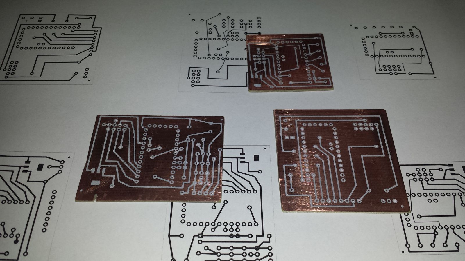
My new pcb's. Smallest for room light, to fit behind wall switch. Second(left) is for kitchen - 3 ds18b20(kitchen temp, fridge temp, and freezer temp), motion sensor, 1602 display, and 2 contact switches for fridge door. Last is for nokia 5110 display, and motion sensor. I can display anything i want on this node.
-
@jendrush said:
My new pcb's.
I noticed that you do top and bottom layer also on connectors.
How do you solder that?I have read a lot about creating your own pcb's and all seem to suggest to use via's...
@marceltrapman said:
I noticed that you do top and bottom layer also on connectors.
How do you solder that?I have read a lot about creating your own pcb's and all seem to suggest to use via's...
I am using VIA too. Only this board for 5110 display have soldering points on both sides becouse display is connected on the one side, rest on the other. Normally all soldering points have to be on one side.
-
I do not remember who started this topic. But this time i will start. Those are my photos from custom PCB production https://www.dropbox.com/sh/ec4ap8dgci1oe0p/AAD3YIqS_JqKMiUFu9TAfF5Ca . This is my second PCB, first was made 12 years ago for school project. I've made few mistakes, but next board will be much much better.
Here is my first attemp at it.
I just started with eagle, so maybe there is room for improvement.
This is for a dimmer node, with some connector for motion detector and light sensor.
It has an onboard 7805 regulator and a mosfet to PWM the leds.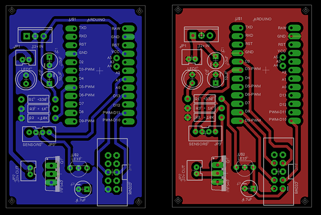
Comments are welcome
-
Here is my first attemp at it.
I just started with eagle, so maybe there is room for improvement.
This is for a dimmer node, with some connector for motion detector and light sensor.
It has an onboard 7805 regulator and a mosfet to PWM the leds.Comments are welcome
-
Here is my first attemp at it.
I just started with eagle, so maybe there is room for improvement.
This is for a dimmer node, with some connector for motion detector and light sensor.
It has an onboard 7805 regulator and a mosfet to PWM the leds.Comments are welcome
-
@ferpando Your's PCB looks more pro than mine:) But designing pcb for home etching is little harder becouse there is no easy way to make double sided soldering points, so every soldering point must be at one side of pcb.
-
@ferpando I would run reset to one of your unused pins at the radio and you have a custom ISP connector.
-
Did you ever produce the board that you have pictured above for the dimmable LED's?
Did it work?
I would be interested in getting 7-10 of these for 12V LED cable lighting applications that I currently have in my home that cannot be supported by conventional Z-Wave dimmers due to the lights being fed from a 120VAC to 12VDC converter. I have made one on a prototype PCB but it is still slightly large for the enclosure and the one you pictured appears that it would fit tidily in the enclosures.
Thx
Vodden
-
@Vodden how large is your enclosure?
I am working on a daughterboard for my mys1.1 with 4 channels of pwm and current measuring on each channel.
each board is 50x50 mm stacked on top of each other.I'm unsure if this solution would work or not. What I am working with is an IKEA Termosfar enclosure. There is very limited room inside and I think that the solution you have proposed wouldn't likely fit.
The prototype board is VERY tight mostly due to the thickness with the pin header installed. The outside dimensions are also critical, with the smallest possible prototype board just barely able to fit. I think the pictured PCB would work perfectly and I have all the parts to build it.
@rosskinard was working on a version of these boards as well but had some issues with the pinout, but I have not heard of any progress on it or if they are available. I was hoping that these ones were available so I could get these lights on dimmers.
-
Hello,
I've been really busy with work and havn't had the time to do some proper testing.
I did assemble a home made board and hope to do some tests soon.
Here's how it looks like: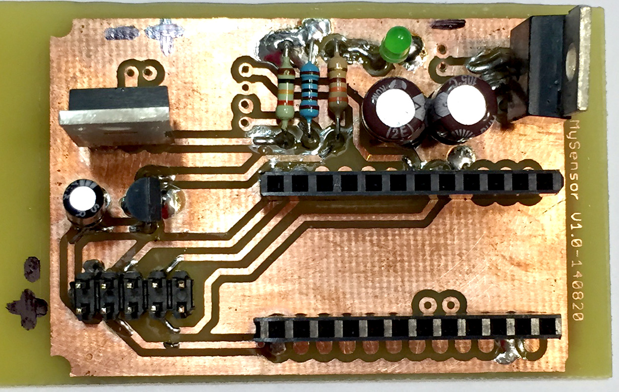
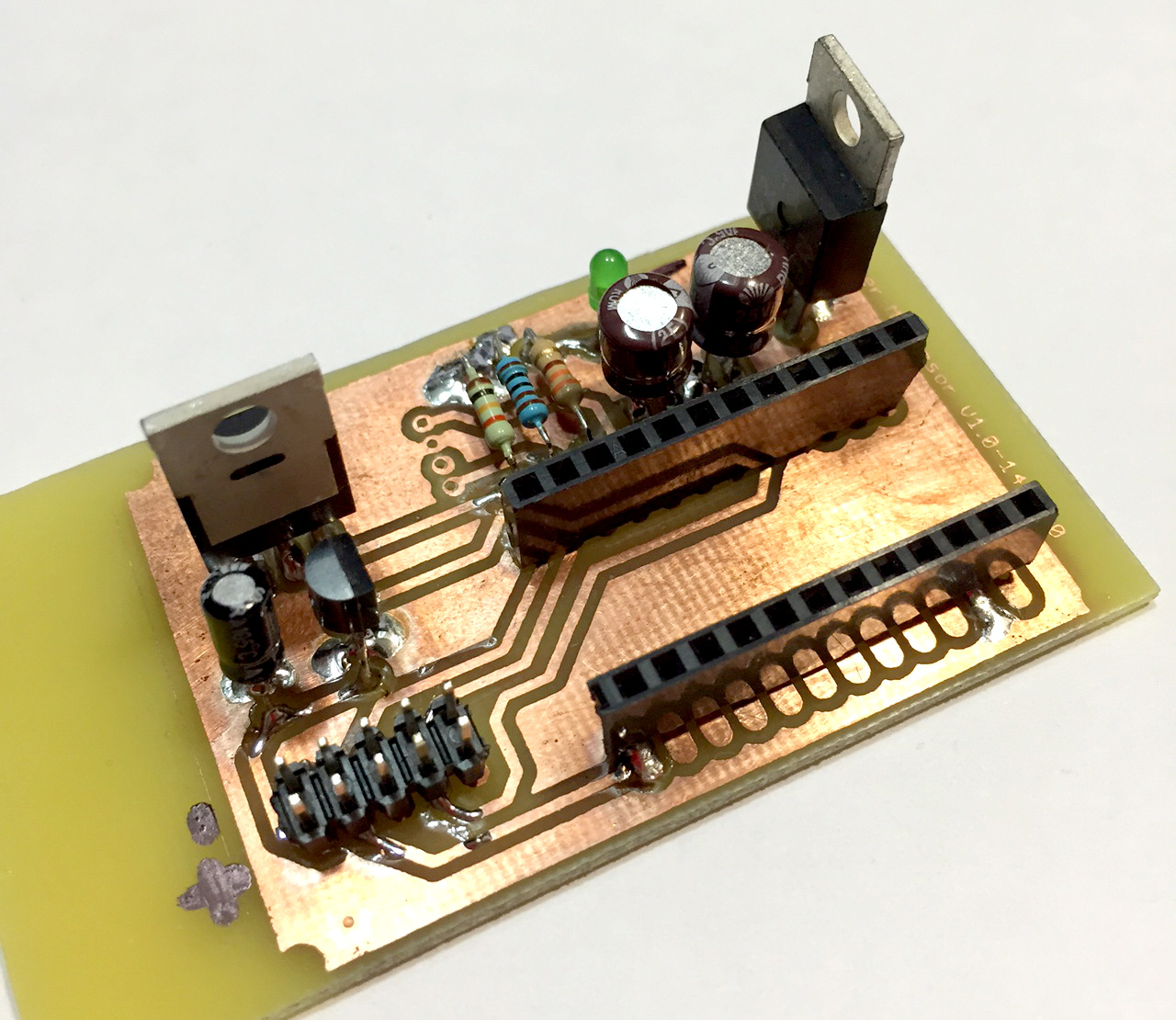
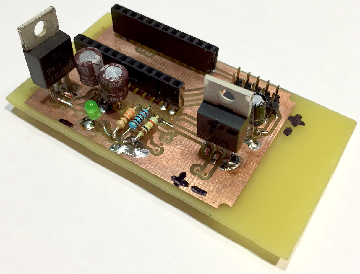
I'll keep you posted
Hello! It looks like you're interested in this conversation, but you don't have an account yet.
Getting fed up of having to scroll through the same posts each visit? When you register for an account, you'll always come back to exactly where you were before, and choose to be notified of new replies (either via email, or push notification). You'll also be able to save bookmarks and upvote posts to show your appreciation to other community members.
With your input, this post could be even better 💗
Register Login