My Slim 2AA Battery Node
-
I know I have many questions :) but how about inverting the nrf position by 180 degree so that it can be on top of the atmega and decrease that length. Would it fit in your design ?
Can you do such board for those who are interested like me :) ?@ahmedadelhosni
I think it's a good idea! And an easy mod, but it's not on priority list atm. Someone else would get a quick start from my already published kicad-files.The thought behind present design is that I didn't want anything to cover the antenna in any direction, but I doubt it would matter much in this suggested case. It'll be worse when it comes to the hight. Look at the photos. The nRF becomes too high for my enclosures if I use a socket, and the 328p with its socket is too high to fit under a nRF without its socket. The solution would be to remove the 328p socket and move the R and Cs to bottom side or somewhere else. And without a 328p socket, the 3x2 AVR ISP pins would become more important to keep. Otherwise the board could have been trimmed even more.
-
@ahmedadelhosni
I think it's a good idea! And an easy mod, but it's not on priority list atm. Someone else would get a quick start from my already published kicad-files.The thought behind present design is that I didn't want anything to cover the antenna in any direction, but I doubt it would matter much in this suggested case. It'll be worse when it comes to the hight. Look at the photos. The nRF becomes too high for my enclosures if I use a socket, and the 328p with its socket is too high to fit under a nRF without its socket. The solution would be to remove the 328p socket and move the R and Cs to bottom side or somewhere else. And without a 328p socket, the 3x2 AVR ISP pins would become more important to keep. Otherwise the board could have been trimmed even more.
@m26872 I guess the nrf above the atmega won't cause problems or interference to the atmega due to rf signals. so that's fine.
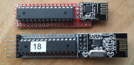
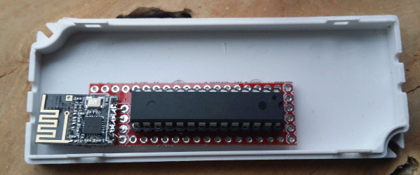
I measured the nrf and it will be 13 mm, so I thought it may fit as from the photos, I guess the max height can be 13 or 14. For me increasing the height is not a problem as I am still searching for cheap compact and not so long enclosure with maximum heigh 20 mm to use. I am searching for cheap products which are kept in that size of enclosure which I need but didn't find it yet :)
I didn't use Kicad before and I guess there is no converters to eagle. Youtube time :)
Can you please tell me the total length of the board + nrf ?
-
@m26872 I guess the nrf above the atmega won't cause problems or interference to the atmega due to rf signals. so that's fine.
I measured the nrf and it will be 13 mm, so I thought it may fit as from the photos, I guess the max height can be 13 or 14. For me increasing the height is not a problem as I am still searching for cheap compact and not so long enclosure with maximum heigh 20 mm to use. I am searching for cheap products which are kept in that size of enclosure which I need but didn't find it yet :)
I didn't use Kicad before and I guess there is no converters to eagle. Youtube time :)
Can you please tell me the total length of the board + nrf ?
@ahmedadelhosni
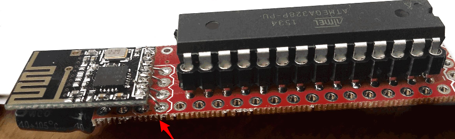
It's 74mm with the angled Arduino pins and 69mm without. -
@ahmedadelhosni
It's 74mm with the angled Arduino pins and 69mm without. -
@m26872 Thanks.
Hopefully this is my last question :)
Is V1.4 and 2.0 the same ? One is red in Eagle and the other in black in Kicad ?
If yes, could you please guide me to the eagle's project files ? Thanks.
@ahmedadelhosni
Yes, v1.4 is Eagle. I'll upload it later today. But it's just a brd-file. And I think I had some broken sch-brd connections even in v1.2. One reason for the KiCad design was to improve this. -
@ahmedadelhosni
Yes, v1.4 is Eagle. I'll upload it later today. But it's just a brd-file. And I think I had some broken sch-brd connections even in v1.2. One reason for the KiCad design was to improve this. -
@m26872 hmm I see. So i will begin learning Kicad today. Thanks for your effort and support
@ahmedadelhosni
I uploaded the brd in the v1.4 post above just for completness.
Happy Kicading! Hope you'll enjoy. I liked it a lot better. There were a few nice youtube tutorials.
You're welcome. -
First Slim Node board donation from the DirtyPCB board share now sent. $12 to MySensors.org. Thanks to everyone that have ordered.
Later credit draw will be in probably linger a bit. DirtyPCB seems to be somewhat of a non-profit community with manual attendance to all share credits. I almost got banned in my attempts to get a reply from them. In order to show my appreciation for their great service, I plan to only request further credits in quantities of 50. If the board not's been shared in a year a so, of course I'll make an exception.
-
I was out of radio's, only a few "smd" types left which I mounted on the board with some patchwork ;-)
Now even more space left in the (small) housing.
-
Could u show a screen for the lockbits too? I have never set them before and need some guidance :D thanks
Dakky
Controller: Raspberry Pi 2 :: Openhab2 :: with @TimO MySensors Binding
Gateway: Arduino MEGA 2560 R3 :: W5100 :: Ethernet GWSoftware: MySensors 2.0development
-
Could u show a screen for the lockbits too? I have never set them before and need some guidance :D thanks
Dakky
-
Is this what you used to burn the bootloader?
-
Just received my boards from DirtyPCB :smile:
Enough for 10x3=30 sensors... :scream: The boards look nice. I think I can even skip the R&C's if I use the internal VCC measuring method but I'll have to scan the thread for that.@martkrui R1 and C2 are mandatory if you intend to use the 6 pin FTDI port (I think you do). C3 (ARef - Gnd) is primarily for when you use Adc external ref, but (if I remember correct) it stabilizes the Adc in general. C1 (Vcc - Gnd) is just the "near chip supply input capacitor" and could probably be left out if there are some other caps near the nRF.
-
Could u show a screen for the lockbits too? I have never set them before and need some guidance :D thanks
Dakky
@dakky said:
Could u show a screen for the lockbits too? I have never set them before and need some guidance :D thanks
Dakky
I use ubuntu, and a tiny USB, so after I have flashed my arduino board, I run this avrdude command, that will run until battery is low
avrdude -c usbtiny -p m328p -U efuse:w:0x07:mI have bought usbtiny from this guy:
http://www.ebay.com/itm/USBtinyISP-V4-AVR-ISP-Programmer-Reliable-Plastic-Enclosure-/330824700564?hash=item4d06b05294 -
@ahmedadelhosni
I think it's a good idea! And an easy mod, but it's not on priority list atm. Someone else would get a quick start from my already published kicad-files.The thought behind present design is that I didn't want anything to cover the antenna in any direction, but I doubt it would matter much in this suggested case. It'll be worse when it comes to the hight. Look at the photos. The nRF becomes too high for my enclosures if I use a socket, and the 328p with its socket is too high to fit under a nRF without its socket. The solution would be to remove the 328p socket and move the R and Cs to bottom side or somewhere else. And without a 328p socket, the 3x2 AVR ISP pins would become more important to keep. Otherwise the board could have been trimmed even more.
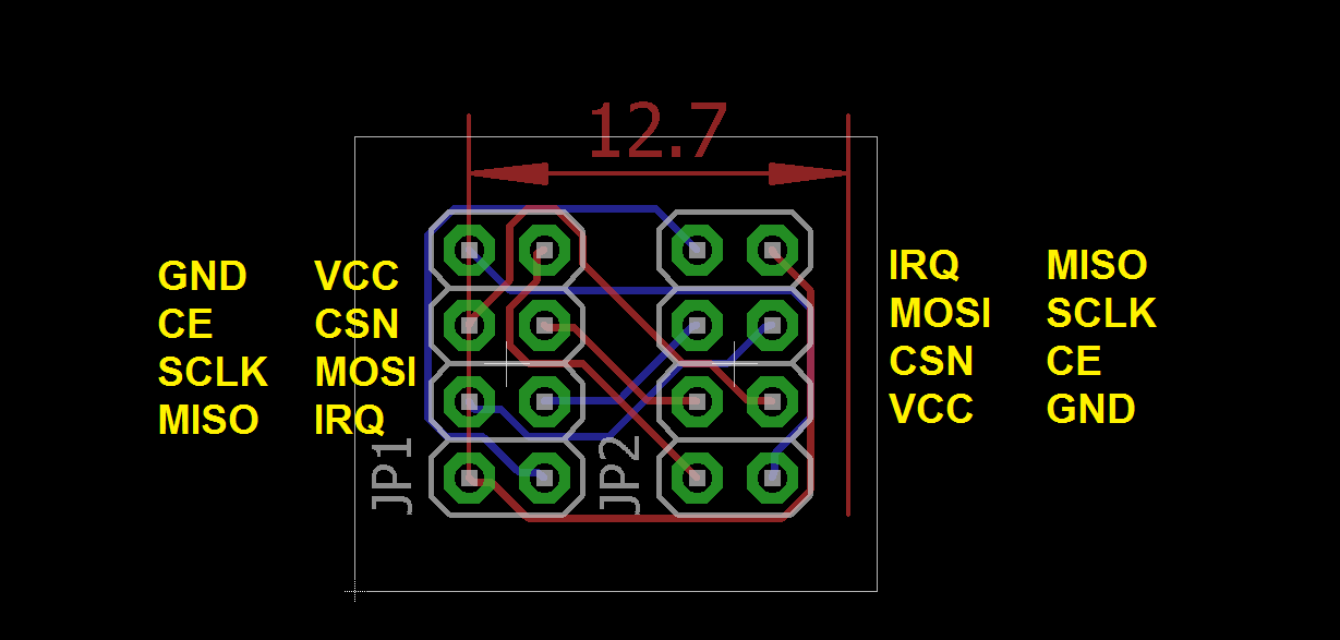
@m26872 Hi again. Just a small update regarding rotating the nrf.
I decided that in my designs I'll need the straight and rotated version, thus I'll design a small board to map the pin outputs like the image below. It will be above the ICSP pins but I really don't care about re flashing.
I'll order the board as soon as I finish pcb layout of some other boards and ship all at once.
Thanks.
-
@m26872 Hi again. Just a small update regarding rotating the nrf.
I decided that in my designs I'll need the straight and rotated version, thus I'll design a small board to map the pin outputs like the image below. It will be above the ICSP pins but I really don't care about re flashing.
I'll order the board as soon as I finish pcb layout of some other boards and ship all at once.
Thanks.
@ahmedadelhosni You know that the nRF pins are not centered? That means if you rotate it like this it will no longer be straight above the "slim node motherboard".
What height do you expect it to be? -
Another "noobish" question:
When using this bootloader, one cycle takes 8 seconds? What happens, if for example, a switch is pressed between? does this sensor detect this?Controller: Raspberry Pi 2 :: Openhab2 :: with @TimO MySensors Binding
Gateway: Arduino MEGA 2560 R3 :: W5100 :: Ethernet GWSoftware: MySensors 2.0development