💬 Adjustable Boost Converter with Pass-Through
-
This project is now finished. :smile:
-
Setting R1=680K gives a voltage output of 2.674v, which is great for charging 2.7v supercaps.
-
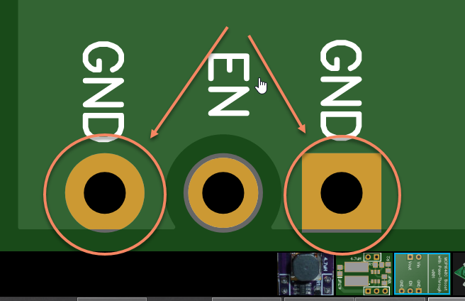
I just now revised the board to expose the Enable pin, so now you can do a pass-through if you wish. I also made it more compact and gave it a ground-plane on the back. Enjoy!
-
i received the upgraded PCB and assembled it. It tests out correctly. The project photo now shows the newest board. Project completed. :)
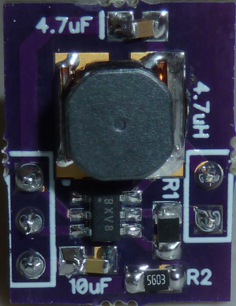
For 3.3v output, use R1=976 ohms and R2=562 ohms, as per the datasheet.
-
i received the upgraded PCB and assembled it. It tests out correctly. The project photo now shows the newest board. Project completed. :)
For 3.3v output, use R1=976 ohms and R2=562 ohms, as per the datasheet.
BTW, the same PCB and circuit can also be used with the MCP1640T instead of the MCP1640C if so desired. In that case, the ENABLE pin acts like an ON/OFF switch, instead of an ON/Pass-through switch.
-
Just little tip from me :) Use thermal relief instead of direct polygon connection.
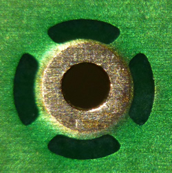
It is much more useful in such cases. -
Just little tip from me :) Use thermal relief instead of direct polygon connection.
It is much more useful in such cases.@Koresh said in 💬 Adjustable Boost Converter with Pass-Through:
Just little tip from me :) Use thermal relief instead of direct polygon connection.
It is much more useful in such cases.Where do I put that exactly?
-
@Koresh said in 💬 Adjustable Boost Converter with Pass-Through:
Just little tip from me :) Use thermal relief instead of direct polygon connection.
It is much more useful in such cases.Where do I put that exactly?
-
Sorry if I'm being dense, but how are the thermal reliefs better? What's their advantage?
-
Sorry if I'm being dense, but how are the thermal reliefs better? What's their advantage?
@NeverDie It is much easier to solder the wire to pads with relief connection than the wire to directly connected pads. Your soldering point even can be unreliable if your pad is directly connected to very huge polygon and your soldering iron don't have enough power.
-
@NeverDie I have got MCP1640CT-I/CHY in SOT-23 (BX5V marking on the chip)
Can these be used for this project please?I also have some 8 pins ones, but there are not suitable
-
@openhardware-io
I am having issues can someone help
I am getting output voltage same as input , i removed enable pin supply still i was getting output voltage same as input what might be the issue?
Hello! It looks like you're interested in this conversation, but you don't have an account yet.
Getting fed up of having to scroll through the same posts each visit? When you register for an account, you'll always come back to exactly where you were before, and choose to be notified of new replies (either via email, or push notification). You'll also be able to save bookmarks and upvote posts to show your appreciation to other community members.
With your input, this post could be even better 💗
Register Login