CNC PCB milling
-
@rmtucker said in CNC PCB milling:
Is it working correctly if you just issue a G0 x10 then x-10?
No, it goes left in both instances.
@rmtucker said in CNC PCB milling:
did you switch to the jpadie workspace for v1.1?
yes
@neverdie sorry, I'm abroad, with very limited availability, so cannot answer too quickly.
based on the mentioned facts it seems to me, that the X axis direction pin is sticked to one position, maybe it has a solder bridge to another pin, or vcc / gnd directly.

-
@neverdie sorry, I'm abroad, with very limited availability, so cannot answer too quickly.
based on the mentioned facts it seems to me, that the X axis direction pin is sticked to one position, maybe it has a solder bridge to another pin, or vcc / gnd directly.
@andrew said in CNC PCB milling:
@neverdie sorry, I'm abroad, with very limited availability, so cannot answer too quickly.
based on the mentioned facts it seems to me, that the X axis direction pin is sticked to one position, maybe it has a solder bridge to another pin, or vcc / gnd directly.
Thanks! You nailed it. It turns out the solder connection on the atmega328p pin corresponding to D5 just wasn't good enough. I resoldered it, and now the X-axis works in both directions. :)
-
I'm receiving this error message now:
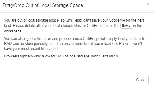
However, it's not obvious how to delete the files it's referring to. Anyone know how? -
Great news! Grbl1.1f makes all the difference. I tried milling at 6 mil separation using the upgraded grbl1.1f, and it works!
There's a huge difference between being able to evolve a single PCB design to perfect it rather than having to work on a "dumbed down" design (for a CNC or some other DIY etching process) before being able to get "the real deal" from a PCB fabricator. So, I'm very relieved that the first option now seems possible. :) -
Great news! Grbl1.1f makes all the difference. I tried milling at 6 mil separation using the upgraded grbl1.1f, and it works!
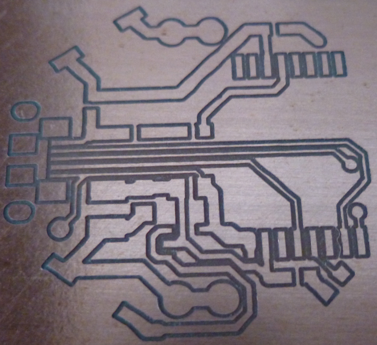
There's a huge difference between being able to evolve a single PCB design to perfect it rather than having to work on a "dumbed down" design (for a CNC or some other DIY etching process) before being able to get "the real deal" from a PCB fabricator. So, I'm very relieved that the first option now seems possible. :)@neverdie as I see from the picture, you can decrease the cutting depth. this could help you to soften the force against the carving bits and it could also help you to use faster feed rates without risking a missing step or bit damage.
btw, what are your currently used parameters?
also, for the best results please be sure, that when you set up the tool width in flatcam, then it is originated from the previously mentioned formula, which uses the carving bit properties (end with + angle) and the cutting depth.
-
@neverdie as I see from the picture, you can decrease the cutting depth. this could help you to soften the force against the carving bits and it could also help you to use faster feed rates without risking a missing step or bit damage.
btw, what are your currently used parameters?
also, for the best results please be sure, that when you set up the tool width in flatcam, then it is originated from the previously mentioned formula, which uses the carving bit properties (end with + angle) and the cutting depth.
@andrew
In this particular instance I had used a dull bit to do the autoleveling at 4mm and then switched to a Jack bit (nominal 0.1mm, 30 degrees) which I re-zeroed before starting the cutting.
Cutting depth: 0.03
Tool width: 0.12mm (just a guess as to the actual width)
Feedrate:80mmIt does seem that the actual cutting depth came out deeper than 0.03mm, so I'm not sure what's up with that. My guess is that the re-zeroing with the sharp bit came out wrong.
-
@neverdie I use a wood screw in the sacrificial board holding a piece of metal as a "clamp" I slide it over the board (1mm overlap) and clip one alligator clip to the screw, the other to the bit. After probing I slide it out of the way. The metal piece is about 10cm long and it's left in place for the life of the wood board.
@executivul said in CNC PCB milling:
The metal piece is about 10cm long and it's left in place for the life of the wood board.
Do you have a photo of that?
Also, are you using double sided tape at all, or is this all that you're doing as far as holding the PCB flat against the sacrificial board?
-
@andrew
Trying to create a double sided PCB, but I am currently stuck on step 3:
I can see that it has created a mirror image which it displays, but I do not see a mirror image gerber object displayed in the project area. That's in contrast to step 4, where when I click "create alignment drill" it does create a drill file that I can see in the project area.Without access to a mirror image gerber object, there's nothing I can select to produce the gcode for the mirror image. So, I'm stuck on this step. How do I gain access to the mirror image gerber object? I've followed the given directions, but so far no joy.
Apparently it doesn't produce a newly named gerber object. Instead, you just work with whatever it has in memory.
-
@andrew
Trying to create a double sided PCB, but I am currently stuck on step 3:
I can see that it has created a mirror image which it displays, but I do not see a mirror image gerber object displayed in the project area. That's in contrast to step 4, where when I click "create alignment drill" it does create a drill file that I can see in the project area.Without access to a mirror image gerber object, there's nothing I can select to produce the gcode for the mirror image. So, I'm stuck on this step. How do I gain access to the mirror image gerber object? I've followed the given directions, but so far no joy.
- I ise Scotch 665 double sided tape and lately I use a heavy item connected to the ground pin when probing. Put it on the pcb and you get the pcb face grounded. The probe pin clips to the bit. I tend to probe using the same bit used for engraving.
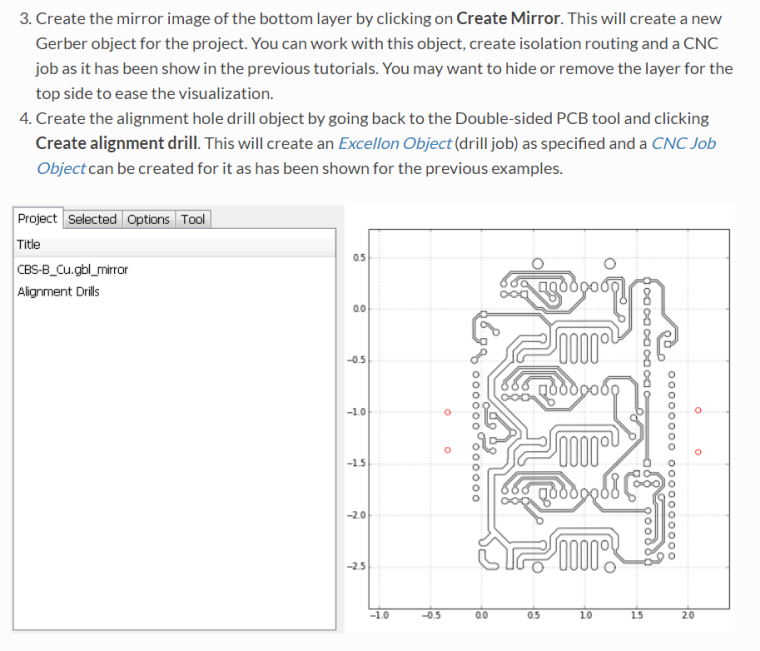
- You select the bottom layer in flatcam. I create a bounding box around it first. Then select the box, the x axis. A few alignment drill locations on one side of the flip line. Hit create aligment drills and hit mirror object which mirrors the already loaded bottom layer (GBL) object. If you watch closely you should see the tracks are mirrored. Then select the object and go on with creating iso geometry and cnc paths.
-
- I ise Scotch 665 double sided tape and lately I use a heavy item connected to the ground pin when probing. Put it on the pcb and you get the pcb face grounded. The probe pin clips to the bit. I tend to probe using the same bit used for engraving.
- You select the bottom layer in flatcam. I create a bounding box around it first. Then select the box, the x axis. A few alignment drill locations on one side of the flip line. Hit create aligment drills and hit mirror object which mirrors the already loaded bottom layer (GBL) object. If you watch closely you should see the tracks are mirrored. Then select the object and go on with creating iso geometry and cnc paths.
@executivul said in CNC PCB milling:
You select the bottom layer in flatcam. I create a bounding box around it first. Then select the box, the x axis. A few alignment drill locations on one side of the flip line. Hit create aligment drills and hit mirror object which mirrors the already loaded bottom layer (GBL) object. If you watch closely you should see the tracks are mirrored. Then select the object and go on with creating iso geometry and cnc paths.
Yes, I think the flatcam's original instructions were faulty. It said to load both the top and bottom layer. Maybe that's fine for selecting pin alignment locations, but there should be only one layer displayed before the mirroring, or else it creates a mess.
Also, I had thought it would create a new file for the mirrored gerber, but it doesn't. Instead, I just work with the mirrored gerber that's in memory to produce the gcode for the mirrored image. I guess that's good enough.
-
I drilled the alignment holes with 0.8mm diameter. I'm using regular male header pins for the alignment, and having tried it, I think 0.8mm is really too tight. Not sure how @andrew is using 0.7mm. Different pins I guess? Anyhow, next time I'll try 0.9mm hole diameter.
-
How do I mill a slot? Do I treat it the same as a regular hole, except use a routing bit rather than a drill bit when it comes time to cut the slot?
-
How do I mill a slot? Do I treat it the same as a regular hole, except use a routing bit rather than a drill bit when it comes time to cut the slot?
@neverdie said in CNC PCB milling:
How do I mill a slot? Do I treat it the same as a regular hole, except use a routing bit rather than a drill bit when it comes time to cut the slot?
Couldn't find a good answer to this, so I'm going to approximate it by simply drilling a series of overlapping holes.
It's needed for the micro-usb connector.
-
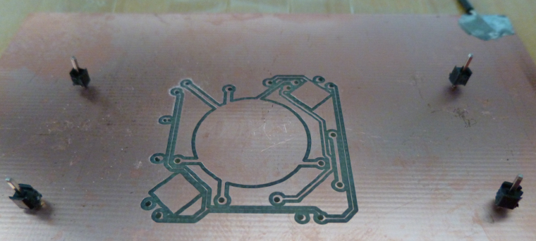
I did the top layer, together with alignment holes, for a real FR4 PCB:
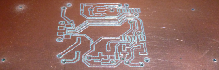
As an experiment, I thought I would standardize on 0.9mm holes for the through-holes, via-holes, and alignment holes, so that there would be fewer tool changes. Looks like it will work, but, meh, I think I'll use smaller via holes in the future.Out of time for today, so I plan to etch the flip side tomorrow.
-
I did the top layer, together with alignment holes, for a real FR4 PCB:
As an experiment, I thought I would standardize on 0.9mm holes for the through-holes, via-holes, and alignment holes, so that there would be fewer tool changes. Looks like it will work, but, meh, I think I'll use smaller via holes in the future.Out of time for today, so I plan to etch the flip side tomorrow.
@neverdie 0.4-0.5mm for vias using 0.3mm silver plated "wrapping wire". 0.9 for TH and alignment holes.
Tomorrow redo the alignment holes on the sacrificial layer so you get perfect alignment (if you don't have homing endstops, as I don't) and put the pins in and sick the pcb after that, be careful how you flip the board, I tend to use asymmetric alignment holes so I can only flip it one way (; -
Argh, it just occurred to me that I was premature in drilling the TH and via holes, because they may seriously interfere with the autoleveling when I etch the reverse side. This must be why @andrew etches the mirrored bottom side first, so that when it's flipped the top side can be etched and then drilled.
-
Re-using the alignment holes already drilled, I flipped over the PCB and etched the mirrored bottom. It worked! Some of the traces are only as thick as a hair, but they all conduct and none are broken.
I guess I'll have to flip it again in order to route the board outline. So, count that as yet another reason to start by etching the bottom first.
I had to autolevel at 6mm in order to dodge all the holes I had prematurely drilled, so perhaps that's why this particular etching came out so uneven.