Skip to content

KiCad

KICad discussions

21 Topics 112 Posts
  • KiCAT 3d shapes not working

    1
    1 Votes
    1 Posts
    83 Views
    No one has replied
  • This topic is deleted!

    1
    0 Votes
    1 Posts
    1 Views
    No one has replied
  • How to customize your schematic symbols for KiCad

    1
    0 Votes
    1 Posts
    736 Views
    No one has replied
  • Kicad library for dc-dc step up booster

    6
    0 Votes
    6 Posts
    2k Views
    B
    @sundberg84 thank you again. I'll do like you say :)
  • Model for arduino Nano

    5
    0 Votes
    5 Posts
    3k Views
    JeaneldredgeJ
    For a very long time I’m looking for an application where the NRF24L01 + will be, but I can’t find it. So if someone tells me I will be grateful.
  • uConfig - automaticly extract component from PDF datasheet to KiCad

    1
    0 Votes
    1 Posts
    2k Views
    No one has replied
  • Interactive KiCAD BoM

    3
    1 Votes
    3 Posts
    979 Views
    monteM
    @hek it's a python script that can be runned standalone from the terminal. By the way it's the only way I could make it work on my system. Apparently some linux versions of KiCad 5 are build without scripting support, so it crashes with segfault when this script is present in kicad's plugin folder. But as a command line script it needs only *.kicad_pcb file as an argument to work.
  • Design a MySensors object with KiCad (french tutorial)

    4
    4 Votes
    4 Posts
    3k Views
    U
    @ericperonnin thanks a lot for the videos, I've just started with KiCad (with PCB design generally speaking) and starting from your tutorial has been an excellent way to get up to speed in a short time!
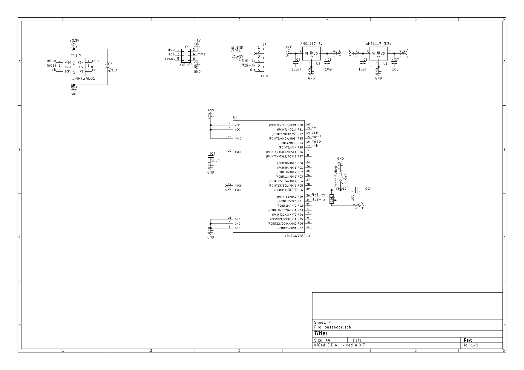
  • Basenode schematic.

    3
    1
    0 Votes
    3 Posts
    1k Views
    F
    Hi, I'm still rather new at this myself, but here are a few questions/remarks: How did you label your connections? I would think you need "global labels" which are surrounded by an arrow like shape in KiCad. Yours look like regular text. Why add +5V and +3.3V labels to your power inputs? They are globally accessible without additional labeling. AMS1117-3.3v datasheet mentions a single tantalum capacitor of 22uF on output only. I'm unsure why you put the other capacitors on those regulators. I used the same regulator and went by the discussion here. You should run the annotation tool and electronic rules check. It will probably complain about the power not being driven. You can solve this by connecting the input power and ground with the PWR_FLAG power symbol. You should mark the unused connections on the MCU with "no connect" cross mark. I hope this helps.
  • Eagle to KiCad converter

    1
    4 Votes
    1 Posts
    2k Views
    No one has replied
  • Footprint with 3d model

    1
    0 Votes
    1 Posts
    2k Views
    No one has replied
  • RFM69HCW SMD footprint?

    2
    0 Votes
    2 Posts
    2k Views
    E
    Answer to myself: There is one from Sparkfun.
  • Drag traces?

    4
    0 Votes
    4 Posts
    2k Views
    E
    @mtiutiu For me, D doesn't do anything at all. m acts as set in the dialog.
  • KiCad Arduino footprint

    Moved
    5
    0 Votes
    5 Posts
    15k Views
    AnticimexA
    FTDI pins are not on the footprint because they are typically used for a connector on the arduino module itself. And having them included in the footprint would unnecessarily complicate routing as it would more or less box in the routs underneath the module.
  • Missing mysensors_XYZ.pretty files

    6
    0 Votes
    6 Posts
    2k Views
    AnticimexA
    Spacing out is done by all, glad it was such a simple "fix" :)
  • Install kicad mysensor components

    Moved
    23
    1 Votes
    23 Posts
    12k Views
    J
    @mfalkvidd Thx, this definitly saves some Google time. ;)
  • KiCad libraries for WS2812B

    Moved
    1
    0 Votes
    1 Posts
    2k Views
    No one has replied
  • New to KiCad

    Moved
    3
    0 Votes
    3 Posts
    2k Views
    tbowmoT
    @dbemowsk Welcome to the wonderful land of kicad :) As already mentioned, we have a kicad parts library on git hub, which we use for the mysensors components. There are setup instructions as well, so you can get started. I think we already have a nano in our repository (I'm not near my computer at the moment so can't check).
  • Software for PCB 3D design

    Moved
    7
    0 Votes
    7 Posts
    3k Views
    hekH
    @Mateusz-Pięta I use PCB Stackup to generate SVGs from the gerber files. The svgs get converted (on the fly) to rasterised images in the browser. I build a model in three.js where I "punch out"/drill holes in the 3d model based on the transparent areas of the rasterised image. I was surprised of the result myself. Here's a gist with the relevant javascript for creating the 3d-object from front/back svgs: https://gist.github.com/henrikekblad/292349f928fe67ff574cb975fdaa7488
  • NRF24L01+ smd schematics

    Moved
    18
    0 Votes
    18 Posts
    11k Views
    tbowmoT
    @emc2 I updated the footprint on github (and yes, I also chose the easy route, and swapped pins 1 and 2 on the footprint) :)

26

Online

11.7k

Users

11.2k

Topics

113.1k

Posts