nRF5 action!
-
I suspect it may be the while statement in this part of the library code that's doing it:
int8_t hwSleep(unsigned long ms) { hwSleepPrepare(ms); while (nrf5_rtc_event_triggered == false) { hwSleep(); } hwSleepEnd(ms); return MY_WAKE_UP_BY_TIMER; } -
I suspect it may be the while statement in this part of the library code that's doing it:
int8_t hwSleep(unsigned long ms) { hwSleepPrepare(ms); while (nrf5_rtc_event_triggered == false) { hwSleep(); } hwSleepEnd(ms); return MY_WAKE_UP_BY_TIMER; }Yup, that was it. I excised the while-loop and re-wrote it as a differently named function, which I now call instead of sleep(..):
int8_t myHwSleep(unsigned long ms)
{
  hwSleepPrepare(ms);
  //while (nrf5_rtc_event_triggered == false) {
    hwSleep();
  //}
  hwSleepEnd(ms);
  return MY_WAKE_UP_BY_TIMER;
}
and it now works "correctly"--well, at least what I want it to do. :) I'll flag it for @d00616, who may have good reasons for keeping it as-is.
-
@d00616 said in nRF5 Bluetooth action!:
It looks like you are implementing a new radio protocol and you are coming forward.
Yes, I'm presently focused on trying to reduce the amount of energy consumed by probably the hardest case of all: a battery/solar/supercap receiver that needs to be both highly responsive (within 100ms) and listening 24/7 without running out of juice. Of course, one can always throw bigger batteries or bigger solar panels at the problem, but I'm first trying to be as ultra efficient as possible so that won't be necessary. The benefit will be smaller size, not to mention lower cost.
I am posting my findings as I go because there is precious little in the way of working examples, so I may yet still be of help to others in that way. From the view count, it does seem that people are reading this thread, even if not many are posting.
-
Epilog: It turns out that the reason I was getting erroneous readings of RSSISAMPLE by the CPU is that the radio must be turned-on when that register is being read. I had hoped it was being stored somewhere else in memory, but it's not. So, probably the best that can be done from an energy standpoint is to have the PPI pipeline the waking of the radio and the CPU from sleep, such that neither is waiting for the other to wake up in order to get work done. Ideally, the moment the RSSI measurement is taken by the PPI, the CPU would have just then fully woken up and be able to evaluate RSSISAMPLE, while the radio is still turned on.
A different approach would be to have the PPI cyclically wake the radio into Rx mode for a period of time and then shut it down. If it received a packet, it would trigger a wake-up on the CPU. This is more or less how the RFM69's "listen mode" works. I may give this a try also so as to measure whether total current consumed is greater or less than the current consumed by the revised RSSI approach (above). I think it might. Although the radio has to remain on longer than it would if it were doing purely an RSSI measurement, it has the advantage that the CPU can remain asleep until an actual packet is received. Given that the radio spends a lot of time just ramping up after being disabled, I'm guessing the incremental Rx time needed for packet detection won't seem so much in comparison. The hard part to this approach will be timing just how long the Radio is in RX mode. Although there are technically three RTC instantiations that can be used, they all share the same prescaler.
So, in order to create a short delay timer, I set one GPIO pin high, which charges a second GPIO pin through a very small capacitor and diode in parallel. Then, when the first GPIO pin goes low, the voltage on the second GPIO pin decays. By setting a PPI event on the second pin to trigger from a Hi2Lo transition, I'm able to create an analog delay, which varies in duration depending on the value of the capacitor. Presently, using a 2.2nF capacitor creates about a 2ms delay between the first pin going LOW and the second pin detecting a Hi2Lo event. It is that event which could be used to trigger turning off the radio after it has listened for packets, whereas it is the first pin going LOW that would have triggered turning on the radio and putting it into RX mode. This is all controlled by the PPI, so no energy needs to be used by the CPU. :)
If anyone can think of a better or more of a digital way to create a predictable time delay, please do post. However, I'm using this method for now just for proof of concept purposes.
-
Here's a scope capture of it:
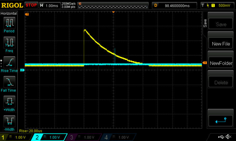
The yellow line shows the rapid charging and then subsequent decay of voltage on the second pin. The blip on the blue line shows that after slightly more than 2ms, the Hi2Lo event was triggered, because the voltage on the second pin had dropped enough for the Hi2Lo transition to occur. As you can see, it happens at around 1v. I was able to capture it on the scope because I used that event to very briefly set a third pin (the one whose voltage is being tracked by the blue line) HIGH.
Again, all of this is being managed by the PPI while the CPU is asleep. :)
-
@NeverDie said in nRF5 Bluetooth action!:
If your goal is to minimize the RX-on time, then you can trigger the RX start and stop by a timer for your minimal window where the frame must be start. Then use the bitcounter top stop the timer in case a packet is received. A shortcut to the end is disabling the RX mode. You can wakeup the CPU with the END event.P.S.: you can reduce the RX/TX time by enabling fast ramp up in MODECNF0 if you haven't to care about nRF51 compatibility.
@d00616 said in nRF5 Bluetooth action!:
@NeverDie said in nRF5 Bluetooth action!:
If your goal is to minimize the RX-on time, then you can trigger the RX start and stop by a timer for your minimal window where the frame must be start. Then use the bitcounter top stop the timer in case a packet is received. A shortcut to the end is disabling the RX mode. You can wakeup the CPU with the END event.P.S.: you can reduce the RX/TX time by enabling fast ramp up in MODECNF0 if you haven't to care about nRF51 compatibility.
Thanks! It finally dawned on me that having the PPI use the RTC's CC registers would be a far better way to schedule turning on and off the radio's RX than using the stopgap analog delay that I had devised (above). Your interrupt handler example helped me see what had been staring me in the face the entire time, but without my recognizing it as the answer to the problem. Funny how that can sometimes happen, where the whole gestalt can just suddenly change. So, thanks again for sharing your example code. This will be a much less awkward solution! :)
-
Where exactly do I look to find all the pin mappings that are assumed for the "Generic nRF52" board? For example, what are the pin numbers that are assumed for RXI, TXO, MISO, MOSI, etc.?
-
I just now posted a source code example and hardware demo for my recently completed breakout board which uses "MyNRF52Board nRF52832" board as the reference when compiling within the Arduino IDE:
https://www.openhardware.io/view/471#tabs-sourceI think from this point forward I'm going to use "MyNRF52Board nRF52832" for any custom boards I develop. Thanks to @d00616, it is a very convenient framework for organizing and enabling the preferred pin mappings. :)
-
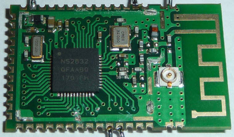
Looks as though the nRF52832 sparkfun board has more of a conventional trace antenna:
though isn't it somewhat odd that it appears to also be directly connected to the ground plane(?), or at least a copper pour. Is that normal? This was one of the images produced by sending their .BRD file to oshpark, so that I could get a look at the antenna.@NeverDie That is a meandered Inverted F Antenna (IFA). It will give you better performance then a standard meandering antenna and a much smaller size then a standard 1/4wave trace antenna. Not as easy to tune however. You can read about the one that TI designed for their 2.4Ghz dongle. http://www.ti.com/lit/an/swra117d/swra117d.pdf
Of course this is not Device dependent as you need to feed it with a 50 ohm feed point. A Pi network before between the Chip's ANT output and the Antenna is desired from a tuning standpoint.Note that on the nRF52 designs, the two components (Cap and Inductor) connected to the ANT pin are used for harmonic filtering AND impedance matching and has nothing to do with the antenna tuning other to present a 50ohm feed point.
-
@NeverDie That is a meandered Inverted F Antenna (IFA). It will give you better performance then a standard meandering antenna and a much smaller size then a standard 1/4wave trace antenna. Not as easy to tune however. You can read about the one that TI designed for their 2.4Ghz dongle. http://www.ti.com/lit/an/swra117d/swra117d.pdf
Of course this is not Device dependent as you need to feed it with a 50 ohm feed point. A Pi network before between the Chip's ANT output and the Antenna is desired from a tuning standpoint.Note that on the nRF52 designs, the two components (Cap and Inductor) connected to the ANT pin are used for harmonic filtering AND impedance matching and has nothing to do with the antenna tuning other to present a 50ohm feed point.
@Jokgi said in nRF5 Bluetooth action!:
@NeverDie That is a meandered Inverted F Antenna (IFA). It will give you better performance then a standard meandering antenna and a much smaller size then a standard 1/4wave trace antenna. Not as easy to tune however. You can read about the one that TI designed for their 2.4Ghz dongle. http://www.ti.com/lit/an/swra117d/swra117d.pdf
Of course this is not Device dependent as you need to feed it with a 50 ohm feed point. A Pi network before between the Chip's ANT output and the Antenna is desired from a tuning standpoint.Note that on the nRF52 designs, the two components (Cap and Inductor) connected to the ANT pin are used for harmonic filtering AND impedance matching and has nothing to do with the antenna tuning other to present a 50ohm feed point.
It looks the same as the antenna on the Ebyte E73-2G4M04S nRF52832 module. Is there any difference? i.e. are you just supplying background information, or are you making a suggestion for improvement?
-
It's not clear whether the DK can/should be used for this part of it, as it's unclear (at least to me) whether it will end up altering the target chip or the DK. I'm just not sure. So, to do at least this ambiguous part of it, I'll first check whether or not the nRFgo studio software will work with one of the other programmers I've collected (not the DK). That may take a while...
@NeverDie nRFgo Studio uses the Segger J-link firmware. When using the Softdevice make sure that your application does not start below the top of the Softdevice or you will get a error on most programmers that there is something located in that protected space. If it does not see this as a protected area then you will corrupt the Softdevice.
Most programmers only need the two SWD lines, ground and a voltage reference from your target board back to the programmer. This is to tell the programmer you have a target board connected and what voltage it is running on. Note that the nRF52-DK does NOT have voltage translators on the programming lines (P19 and P20) so you must be powering your target boards with 3vdc to 3.3vdc. (I have tested down to 2.8vdc but it is not guaranteed to work consistently.) Not sure about ST or other programmers.
-
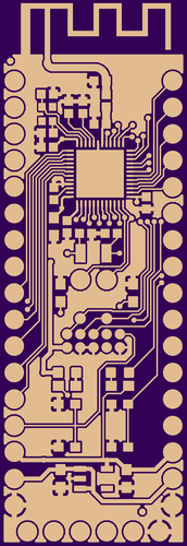
Here's a photo with the lid pried off:
Maybe we can reconstruct what's going on just from looking at the components and the trace lines? At least for now, I'm not so concerned with the RF part.@NeverDie someone did not read the datasheet. The harmonic filter / impedance matching network on the output of Pin 30 (ANT) is connected incorrectly. There needs to be abolded text Cap from ANT out to Pin 31 ONLY. (Not connected to any other ground pour as it seems they did here. Seems to be a few "extra components between there and the Antenna matching network too.
From the nRF52832 datasheet.
bolded text53.8 PCB layout example
The PCB layout shown below is a reference layout for the QFN package with internal LDO setup.
Important: Pay attention to how the capacitor C3 is grounded. It is not directly connected to the
ground plane, but grounded via VSS pin 31. This is done to create additional filtering of harmonic
components.[link text](link url) -
@Jokgi said in nRF5 Bluetooth action!:
@NeverDie That is a meandered Inverted F Antenna (IFA). It will give you better performance then a standard meandering antenna and a much smaller size then a standard 1/4wave trace antenna. Not as easy to tune however. You can read about the one that TI designed for their 2.4Ghz dongle. http://www.ti.com/lit/an/swra117d/swra117d.pdf
Of course this is not Device dependent as you need to feed it with a 50 ohm feed point. A Pi network before between the Chip's ANT output and the Antenna is desired from a tuning standpoint.Note that on the nRF52 designs, the two components (Cap and Inductor) connected to the ANT pin are used for harmonic filtering AND impedance matching and has nothing to do with the antenna tuning other to present a 50ohm feed point.
It looks the same as the antenna on the Ebyte E73-2G4M04S nRF52832 module. Is there any difference? i.e. are you just supplying background information, or are you making a suggestion for improvement?
@NeverDie Pretty much a reference only. In a previous post you inquired about the grounding on the meandering antenna. I posted the TI application note as a frame of reference only. However if you do create your own module you should be aware that the two matching components coming off the ANT pin are NOT antenna matching components but are three for output impedance matching and also acts as a low pass filter. Pi network is still required for tuning of the antenna. (may not use all three components after tuning)
-
@NeverDie nRFgo Studio uses the Segger J-link firmware. When using the Softdevice make sure that your application does not start below the top of the Softdevice or you will get a error on most programmers that there is something located in that protected space. If it does not see this as a protected area then you will corrupt the Softdevice.
Most programmers only need the two SWD lines, ground and a voltage reference from your target board back to the programmer. This is to tell the programmer you have a target board connected and what voltage it is running on. Note that the nRF52-DK does NOT have voltage translators on the programming lines (P19 and P20) so you must be powering your target boards with 3vdc to 3.3vdc. (I have tested down to 2.8vdc but it is not guaranteed to work consistently.) Not sure about ST or other programmers.
@Jokgi said in nRF5 Bluetooth action!:
you must be powering your target boards with 3vdc to 3.3vdc. (I have tested down to 2.8vdc but it is not guaranteed to work consistently.) Not sure about ST or other programmers.
Thanks for reminding me of this. It turns out to be true for the J-Link programmers which are for sale on Aliexpress.com as well.
-
@Jokgi said in nRF5 Bluetooth action!:
you must be powering your target boards with 3vdc to 3.3vdc. (I have tested down to 2.8vdc but it is not guaranteed to work consistently.) Not sure about ST or other programmers.
Thanks for reminding me of this. It turns out to be true for the J-Link programmers which are for sale on Aliexpress.com as well.
@NeverDie I am not sure about all the boards for sell on that site. but I would have to say that any J-link programmer that is packaged as such for $12-$40 dollars is probably counterfeit. Updating these items with newer J-link firmware would more then likely disable them. (On purpose) You may wish to contact Segger in Boston prior to spending money on these potential clones. I would be interested to hear what experiences other people have had with the products from that site.
The genuine J-link and j-link plus programmers are over $400.00 as you can see on the Digi-Key website. Per the Segger license agreements, the only J-link 0B devices that are able to be sold are to be bundled with a Evaluation / Development kit such as the nRF52-DK, ST, Rigato, and other semiconductor / module manufacture's dev kits.
-
@NeverDie I am not sure about all the boards for sell on that site. but I would have to say that any J-link programmer that is packaged as such for $12-$40 dollars is probably counterfeit. Updating these items with newer J-link firmware would more then likely disable them. (On purpose) You may wish to contact Segger in Boston prior to spending money on these potential clones. I would be interested to hear what experiences other people have had with the products from that site.
The genuine J-link and j-link plus programmers are over $400.00 as you can see on the Digi-Key website. Per the Segger license agreements, the only J-link 0B devices that are able to be sold are to be bundled with a Evaluation / Development kit such as the nRF52-DK, ST, Rigato, and other semiconductor / module manufacture's dev kits.
@Jokgi said in nRF5 Bluetooth action!:
@NeverDie I am not sure about all the boards for sell on that site. but I would have to say that any J-link programmer that is packaged as such for $12-$40 dollars is probably counterfeit. Updating these items with newer J-link firmware would more then likely disable them. (On purpose) You may wish to contact Segger in Boston prior to spending money on these potential clones. I would be interested to hear what experiences other people have had with the products from that site.
The genuine J-link and j-link plus programmers are over $400.00 as you can see on the Digi-Key website. Per the Segger license agreements, the only J-link 0B devices that are able to be sold are to be bundled with a Evaluation / Development kit such as the nRF52-DK, ST, Rigato, and other semiconductor / module manufacture's dev kits.
When would I need to upgrade the firmware? At least for now it seems to work just fine.
-
@NeverDie I am not sure about all the boards for sell on that site. but I would have to say that any J-link programmer that is packaged as such for $12-$40 dollars is probably counterfeit. Updating these items with newer J-link firmware would more then likely disable them. (On purpose) You may wish to contact Segger in Boston prior to spending money on these potential clones. I would be interested to hear what experiences other people have had with the products from that site.
The genuine J-link and j-link plus programmers are over $400.00 as you can see on the Digi-Key website. Per the Segger license agreements, the only J-link 0B devices that are able to be sold are to be bundled with a Evaluation / Development kit such as the nRF52-DK, ST, Rigato, and other semiconductor / module manufacture's dev kits.
@Jokgi said in nRF5 Bluetooth action!:
@NeverDie I am not sure about all the boards for sell on that site. but I would have to say that any J-link programmer that is packaged as such for $12-$40 dollars is probably counterfeit. Updating these items with newer J-link firmware would more then likely disable them. (On purpose)
Yes they are of course counterfeit, and using old firmware. You have a message when you use them with Segger software asking you to upgrade to newer firmware and if you accept your programmer is disabled (web is full of solutions to reflash a firmware).
But if you don't upgrade the firmware it works fine as a SWD programmer, at least for basic use (programming). I have not tried any debugging.