💬 Easy/Newbie PCB for MySensors
-
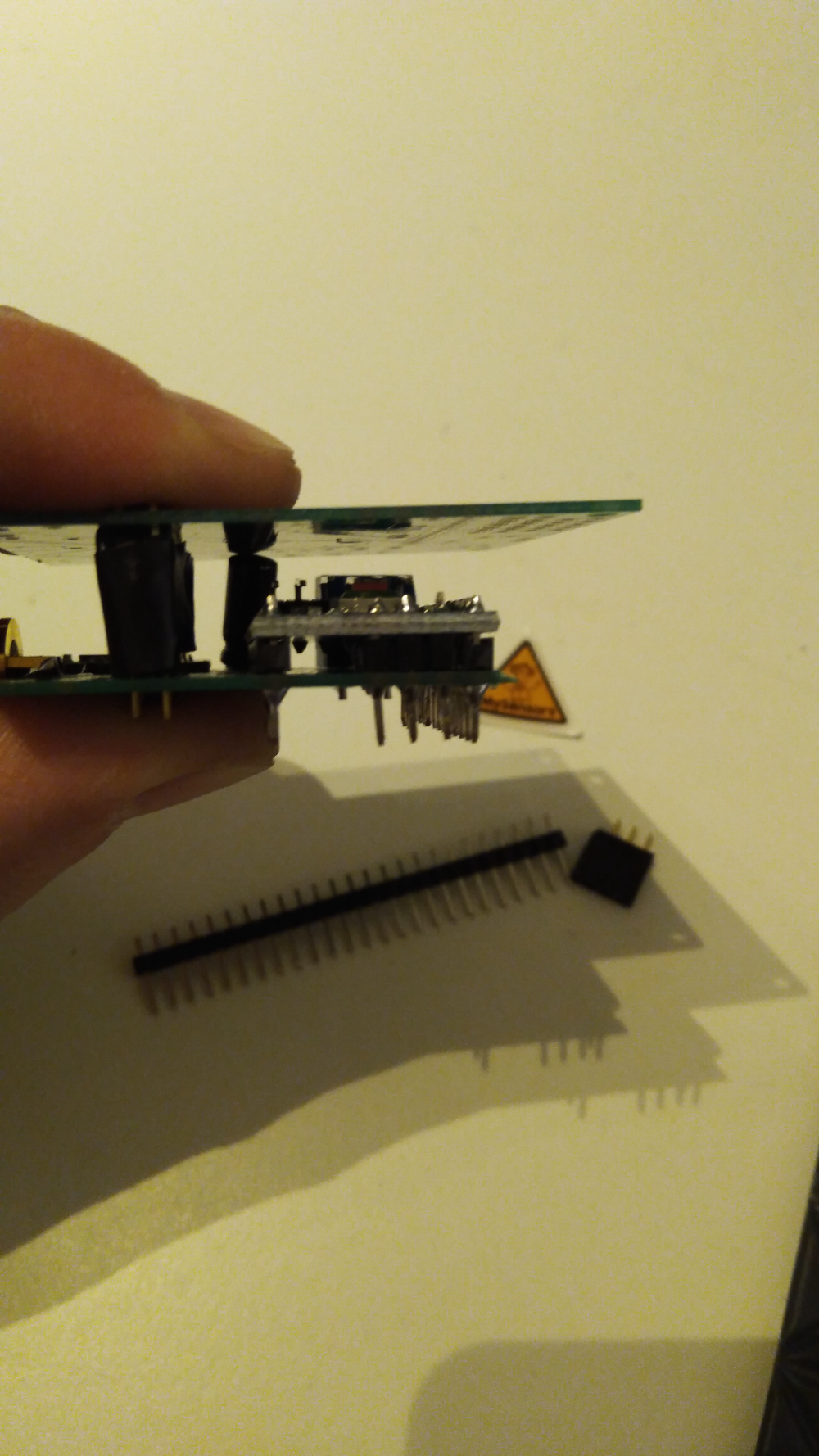
@sundberg84 Well I tried that but did not get the measurement straight from the pcb si I decided t solder a new board using the right capacitor this time (0,1uf instead of 1uf) made sure using the right resistors as well and adding a capacitor after the booster. Than with the same mini pro from the other board tested again and wow it is working as intended.
Child ID 2Battery Voltage: 3.44 V
Battery Percent: 102 %
2930 TSF:MSG:SEND,2-2-0-0,s=255,c=3,t=0,pt=1,l=1,sg=0,ft=0,st=OK:102
2938 MCO:SLP:MS=60000,SMS=0,I1=255,M1=255,I2=255,M2=255
2945 TSF:TDI:TSL
2947 MCO:SLP:WUP=-1
2949 TSF:TRI:TSB
3065 TSF:MSG:SEND,2-2-0-0,s=1,c=1,t=0,pt=7,l=5,sg=0,ft=0,st=OK:998.0
T: 998.00
3178 TSF:MSG:SEND,2-2-0-0,s=0,c=1,t=1,pt=7,l=5,sg=0,ft=0,st=OK:998.0
H: 998.00
957
Child ID 2Battery Voltage: 3.22 V
Battery Percent: 95 %
3690 TSF:MSG:SEND,2-2-0-0,s=255,c=3,t=0,pt=1,l=1,sg=0,ft=0,st=OK:95
3698 MCO:SLP:MS=60000,SMS=0,I1=255,M1=255,I2=255,M2=255
3704 TSF:TDI:TSL
3706 MCO:SLP:WUP=-1
3708 TSF:TRI:TSB
3815 TSF:MSG:SEND,2-2-0-0,s=1,c=1,t=0,pt=7,l=5,sg=0,ft=0,st=OK:998.0
T: 998.00
3932 TSF:MSG:SEND,2-2-0-0,s=0,c=1,t=1,pt=7,l=5,sg=0,ft=0,st=OK:998.0
H: 998.00
955
Child ID 2Battery Voltage: 3.21 V
Battery Percent: 95 %
4442 MCO:SLP:MS=60000,SMS=0,I1=255,M1=255,I2=255,M2=255
4452 TSF:TDI:TSL
4454 MCO:SLP:WUP=-1
4456 TSF:TRI:TSB
4560 TSF:MSG:SEND,2-2-0-0,s=1,c=1,t=0,pt=7,l=5,sg=0,ft=0,st=OK:998.0
T: 998.00
4673 TSF:MSG:SEND,2-2-0-0,s=0,c=1,t=1,pt=7,l=5,sg=0,ft=0,st=OK:998.0
H: 998.00
953
Child ID 2Battery Voltage: 3.21 V
Battery Percent: 95 %
5185 MCO:SLP:MS=60000,SMS=0,I1=255,M1=255,I2=255,M2=255
5193 TSF:TDI:TSL
5195 MCO:SLP:WUP=-1
5197 TSF:TRI:TSB
5304 TSF:MSG:SEND,2-2-0-0,s=1,c=1,t=0,pt=7,l=5,sg=0,ft=0,st=OK:998.0
T: 998.00
5416 TSF:MSG:SEND,2-2-0-0,s=0,c=1,t=1,pt=7,l=5,sg=0,ft=0,st=OK:998.0
H: 998.00
952
Child ID 2Battery Voltage: 3.20 V
Battery Percent: 95 %
5926 MCO:SLP:MS=60000,SMS=0,I1=255,M1=255,I2=255,M2=255
5935 TSF:TDI:TSL
5939 MCO:SLP:WUP=-1
5941 TSF:TRI:TSB
6045 TSF:MSG:SEND,2-2-0-0,s=1,c=1,t=0,pt=7,l=5,sg=0,ft=0,st=OK:998.0
T: 998.00
6158 TSF:MSG:SEND,2-2-0-0,s=0,c=1,t=1,pt=7,l=5,sg=0,ft=0,st=OK:998.0
H: 998.00
952
Child ID 2Battery Voltage: 3.20 V
Battery Percent: 95 %
6670 MCO:SLP:MS=60000,SMS=0,I1=255,M1=255,I2=255,M2=255
6678 TSF:TDI:TSL
6680 MCO:SLP:WUP=-1
6682 TSF:TRI:TSB
6789 TSF:MSG:SEND,2-2-0-0,s=1,c=1,t=0,pt=7,l=5,sg=0,ft=0,st=OK:998.0
T: 998.00
6901 TSF:MSG:SEND,2-2-0-0,s=0,c=1,t=1,pt=7,l=5,sg=0,ft=0,st=OK:998.0
H: 998.00
952
Child ID 2Battery Voltage: 3.20 V
Battery Percent: 95 %
7411 MCO:SLP:MS=60000,SMS=0,I1=255,M1=255,I2=255,M2=255
7419 TSF:TDI:TSL
7424 MCO:SLP:WUP=-1
7426 TSF:TRI:TSB
7530 TSF:MSG:SEND,2-2-0-0,s=1,c=1,t=0,pt=7,l=5,sg=0,ft=0,st=OK:998.0
T: 998.00
7643 TSF:MSG:SEND,2-2-0-0,s=0,c=1,t=1,pt=7,l=5,sg=0,ft=0,st=OK:998.0
H: 998.00
952
Child ID 2Battery Voltage: 3.20 V
Battery Percent: 95 %
8155 MCO:SLP:MS=60000,SMS=0,I1=255,M1=255,I2=255,M2=255
8163 TSF:TDI:TSL
8165 MCO:SLP:WUP=-1
8167 TSF:TRI:TSB
8273 TSF:MSG:SEND,2-2-0-0,s=1,c=1,t=0,pt=7,l=5,sg=0,ft=0,st=OK:998.0
T: 998.00
8388 TSF:MSG:SEND,2-2-0-0,s=0,c=1,t=1,pt=7,l=5,sg=0,ft=0,st=OK:998.0
H: 998.00
955
Child ID 2Battery Voltage: 3.21 V
Battery Percent: 95 %
8898 MCO:SLP:MS=60000,SMS=0,I1=255,M1=255,I2=255,M2=255
8908 TSF:TDI:TSL
8910 MCO:SLP:WUP=-1
8912 TSF:TRI:TSB
9021 TSF:MSG:SEND,2-2-0-0,s=1,c=1,t=0,pt=7,l=5,sg=0,ft=0,st=OK:998.0
T: 998.00
9132 TSF:MSG:SEND,2-2-0-0,s=0,c=1,t=1,pt=7,l=5,sg=0,ft=0,st=OK:998.0
H: 998.00
948
Child ID 2Battery Voltage: 3.19 V
Battery Percent: 94 %
9646 TSF:MSG:SEND,2-2-0-0,s=255,c=3,t=0,pt=1,l=1,sg=0,ft=0,st=OK:94
9654 MCO:SLP:MS=60000,SMS=0,I1=255,M1=255,I2=255,M2=255
9660 TSF:TDI:TSL
9662 MCO:SLP:WUP=-1
9664 TSF:TRI:TSB
9771 TSF:MSG:SEND,2-2-0-0,s=1,c=1,t=0,pt=7,l=5,sg=0,ft=0,st=OK:998.0
T: 998.00
9881 TSF:MSG:SEND,2-2-0-0,s=0,c=1,t=1,pt=7,l=5,sg=0,ft=0,st=OK:998.0
H: 998.00
952
Child ID 2Battery Voltage: 3.20 V
Battery Percent: 95 %
10395 TSF:MSG:SEND,2-2-0-0,s=255,c=3,t=0,pt=1,l=1,sg=0,ft=0,st=OK:95
10403 MCO:SLP:MS=60000,SMS=0,I1=255,M1=255,I2=255,M2=255
10409 TSF:TDI:TSL
10412 MCO:SLP:WUP=-1
10414 TSF:TRI:TSB
10520 TSF:MSG:SEND,2-2-0-0,s=1,c=1,t=0,pt=7,l=5,sg=0,ft=0,st=OK:998.0
T: 998.00
10635 TSF:MSG:SEND,2-2-0-0,s=0,c=1,t=1,pt=7,l=5,sg=0,ft=0,st=OK:998.0
H: 998.00
953
Child ID 2Battery Voltage: 3.21 V
Battery Percent: 95 %
11147 MCO:SLP:MS=60000,SMS=0,I1=255,M1=255,I2=255,M2=255
11155 TSF:TDI:TSL
Now in mqtt I can see the percentage as:
95 qos : 0, retain : false, cmd : publish, dup : false, topic : **mygateway1-out/2/255/3/0/0**, messageId : , length : 30, Raw payload : 5753``` But not the voltage?@mr_sensor good to hear its working.
It looks like you are only sending the % and not the voltage? -
@Mr_sensor It happened to me once that capacitor was just shortening the circuit, it was a smd, but when I removed it and tested it it was constantly making shortage, thus the circuit was never working and luckily my power supply had a low enough protection.
I examined cap very closely, all looked fine, but internally it was not working fine.Since most of us (well, me at least) are buying cheap components I made it a habit now to always measure every passive component before installation, partly eliminates one variable
-
A short sneak-peak on the upcoming revision...
Still a long way to go...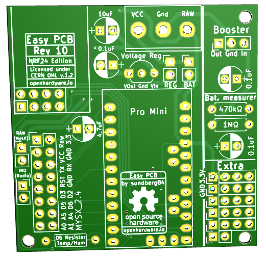
Rev 10 - Nrf24l01+ ed.
- Completley redesigned in KiCad.
- MysX location changed to accept more MysX boards and align like RFM version.
- Optional signing added
- Optional SPI flash added.
- Extra pins aligned to 2.45 vertical & horisontal
- Relocated Extra + Bat Measurer some to allow more space to booster
- Changed pull-up resistor from D3 to D5 to have one more pin for Interrupt
- Relocated D5 pullup, MysX and IRQ jumper some.
- Changed footprint (silk-screen) on capacitor to easier show Gnd/Pos side.
Need to change footprint on voltage regulator on both nrf and rfm edition back to a square and not a liniar one. (rev 9 change). Not intended to revert back.
Also a bit worried the 4,7uF cap os to far away from radio.
Controller: Proxmox VM - Home Assistant
MySensors GW: Arduino Uno - W5100 Ethernet, Gw Shield Nrf24l01+ 2,4Ghz
MySensors GW: Arduino Uno - Gw Shield RFM69, 433mhz
RFLink GW - Arduino Mega + RFLink Shield, 433mhz -
A short sneak-peak on the upcoming revision...
Still a long way to go...Rev 10 - Nrf24l01+ ed.
- Completley redesigned in KiCad.
- MysX location changed to accept more MysX boards and align like RFM version.
- Optional signing added
- Optional SPI flash added.
- Extra pins aligned to 2.45 vertical & horisontal
- Relocated Extra + Bat Measurer some to allow more space to booster
- Changed pull-up resistor from D3 to D5 to have one more pin for Interrupt
- Relocated D5 pullup, MysX and IRQ jumper some.
- Changed footprint (silk-screen) on capacitor to easier show Gnd/Pos side.
Need to change footprint on voltage regulator on both nrf and rfm edition back to a square and not a liniar one. (rev 9 change). Not intended to revert back.
Also a bit worried the 4,7uF cap os to far away from radio.
@sundberg84 said in 💬 Easy/Newbie PCB for MySensors:
Also a bit worried the 4,7uF cap os to far away from radio.
Putting it underneath the nrf24 module? I know it is not a "clean solution" but there would be still be unused space under the radio module
-
@sundberg84 said in 💬 Easy/Newbie PCB for MySensors:
Also a bit worried the 4,7uF cap os to far away from radio.
Putting it underneath the nrf24 module? I know it is not a "clean solution" but there would be still be unused space under the radio module
@gohan - thanks, not what I want to do - I have descided to have optional/more advanced on bottom side. This is the core idea of the PCB. I might revert back to Rev 9 footprint and squeeze it in like prev. revision.
-
A short sneak-peak on the upcoming revision...
Still a long way to go...Rev 10 - Nrf24l01+ ed.
- Completley redesigned in KiCad.
- MysX location changed to accept more MysX boards and align like RFM version.
- Optional signing added
- Optional SPI flash added.
- Extra pins aligned to 2.45 vertical & horisontal
- Relocated Extra + Bat Measurer some to allow more space to booster
- Changed pull-up resistor from D3 to D5 to have one more pin for Interrupt
- Relocated D5 pullup, MysX and IRQ jumper some.
- Changed footprint (silk-screen) on capacitor to easier show Gnd/Pos side.
Need to change footprint on voltage regulator on both nrf and rfm edition back to a square and not a liniar one. (rev 9 change). Not intended to revert back.
Also a bit worried the 4,7uF cap os to far away from radio.
@sundberg84 said in 💬 Easy/Newbie PCB for MySensors:
- MysX location changed to accept more MysX boards and align like RFM version.
Please don't do like that and follow the guideline for the MYSX connector (location was already wrong in previous versions and it's a bit annoying to make MYSX boards for Easy PCB):
*"The MYSX connector should be placed close to the board edge with a 100 mil spacing from all edges. The footprint has a courtyard outline to emphasize this"Also a bit worried the 4,7uF cap os to far away from radio.
I agree especially with other traces to cross before reaching the radio.
-
@sundberg84 said in 💬 Easy/Newbie PCB for MySensors:
- MysX location changed to accept more MysX boards and align like RFM version.
Please don't do like that and follow the guideline for the MYSX connector (location was already wrong in previous versions and it's a bit annoying to make MYSX boards for Easy PCB):
*"The MYSX connector should be placed close to the board edge with a 100 mil spacing from all edges. The footprint has a courtyard outline to emphasize this"Also a bit worried the 4,7uF cap os to far away from radio.
I agree especially with other traces to cross before reaching the radio.
@nca78 said in 💬 Easy/Newbie PCB for MySensors:
@sundberg84 said in 💬 Easy/Newbie PCB for MySensors:
- MysX location changed to accept more MysX boards and align like RFM version.
Please don't do like that and follow the guideline for the MYSX connector (location was already wrong in previous versions and it's a bit annoying to make MYSX boards for Easy PCB):
*"The MYSX connector should be placed close to the board edge with a 100 mil spacing from all edges. The footprint has a courtyard outline to emphasize this"I actually had a long discussion with @Anticimex which is the designer of MysX and he said it is not wrong. Can you please explain why it's wrong ?
I was thinking pin 1 should go towards both vertical and horizontal edge of the pcb (that's why I asked him because I though It should go where the radio is) but he said the only rule is pin 1 should go towards the edge. I looked at the rules and that is what it said so I don't think I'm breaking any rules.
The MYSX connector should be placed close to the board edge with a 100 mil spacing from all edges.
The footprint has a courtyard outline to emphasize this.
It should be oriented so that pin1 is always closest to the board edge parallel to the connector.
This allows a daughter board designed using the same constraints to be facing back "inwards" over the motherboard
Either way it has changed like less than 1mm
If we can somehow get Anticimex to recommend and we can agree on a better placement I'm happy to re-think my design.
If you thinks it's hard to create MysX boards for EasyPcb I have created a finished Kicad project with board outlines, connector and drill holes you can use as a template. Check it out on the project page.
Controller: Proxmox VM - Home Assistant
MySensors GW: Arduino Uno - W5100 Ethernet, Gw Shield Nrf24l01+ 2,4Ghz
MySensors GW: Arduino Uno - Gw Shield RFM69, 433mhz
RFLink GW - Arduino Mega + RFLink Shield, 433mhz -
@nca78 said in 💬 Easy/Newbie PCB for MySensors:
@sundberg84 said in 💬 Easy/Newbie PCB for MySensors:
- MysX location changed to accept more MysX boards and align like RFM version.
Please don't do like that and follow the guideline for the MYSX connector (location was already wrong in previous versions and it's a bit annoying to make MYSX boards for Easy PCB):
*"The MYSX connector should be placed close to the board edge with a 100 mil spacing from all edges. The footprint has a courtyard outline to emphasize this"I actually had a long discussion with @Anticimex which is the designer of MysX and he said it is not wrong. Can you please explain why it's wrong ?
I was thinking pin 1 should go towards both vertical and horizontal edge of the pcb (that's why I asked him because I though It should go where the radio is) but he said the only rule is pin 1 should go towards the edge. I looked at the rules and that is what it said so I don't think I'm breaking any rules.
The MYSX connector should be placed close to the board edge with a 100 mil spacing from all edges.
The footprint has a courtyard outline to emphasize this.
It should be oriented so that pin1 is always closest to the board edge parallel to the connector.
This allows a daughter board designed using the same constraints to be facing back "inwards" over the motherboard
Either way it has changed like less than 1mm
If we can somehow get Anticimex to recommend and we can agree on a better placement I'm happy to re-think my design.
If you thinks it's hard to create MysX boards for EasyPcb I have created a finished Kicad project with board outlines, connector and drill holes you can use as a template. Check it out on the project page.
@sundberg84 I cannot see anything wrong with the MYSX placement on that board.
If one could pick freely, ideal placement of the connector would be in the middle of the board side to allow daughter boards to extend both "upward" and "downward".
But the important rule is the one already cited, that pin1 is oriented to ensure daughterboard orientation relative to the motherboard and that there is spacing around the connector so that the daughterboard female connector does not come in contact with main board cirquitry.
Also that the daughterboard does not protrude outside of the mainboard at least along the edge the connector is aligned to.
Daughterboards in general should not be designed to be wider than the MYSX connector used for this reason (avoiding daughterboard protruding outside mainboard area) to allow a mainboard specific case to be reused with daughterboards mounted.Edit: if possible, try to move the components right next to the connector. (remember the 100mil spacing). The resistor below can probably be mounted on the reverse side.
-
@sundberg84 I will just go ahead and update the spec. Yes, it may cause some existing designs to violate the spec, but that will always be the case. We look forwards, not backwards :)
Spec is here.Back to the drawing desk! :)
Edit: MysX alignment changed so PCB needs to be redesigned.
-
I have moved the discussion about the alignment here :
https://forum.mysensors.org/topic/9060/mysx-connector-alignment -
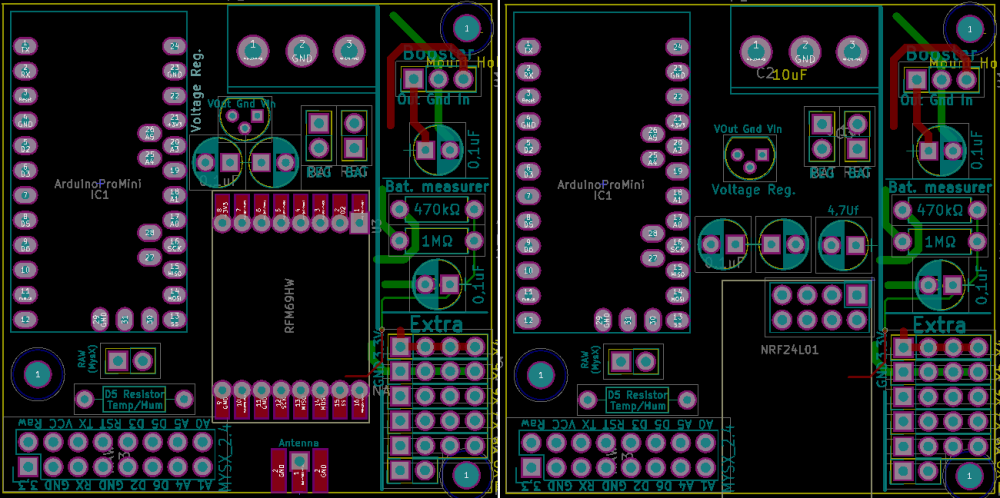
Thoughs? (Noth Nrf + RFM)
@Nca78 - MysX alignment?Controller: Proxmox VM - Home Assistant
MySensors GW: Arduino Uno - W5100 Ethernet, Gw Shield Nrf24l01+ 2,4Ghz
MySensors GW: Arduino Uno - Gw Shield RFM69, 433mhz
RFLink GW - Arduino Mega + RFLink Shield, 433mhz -
Thoughs? (Noth Nrf + RFM)
@Nca78 - MysX alignment?@sundberg84 be careful about daughterboards colliding with the pro mini.
Do you feel secure today? No? Start requiring some signatures and feel better tomorrow ;)
-
@sundberg84 be careful about daughterboards colliding with the pro mini.
@anticimex - thanks for input. Same with radio I guess... ? Don't know how to solve it by fitting all these things into one board.
Controller: Proxmox VM - Home Assistant
MySensors GW: Arduino Uno - W5100 Ethernet, Gw Shield Nrf24l01+ 2,4Ghz
MySensors GW: Arduino Uno - Gw Shield RFM69, 433mhz
RFLink GW - Arduino Mega + RFLink Shield, 433mhz -
@anticimex - thanks for input. Same with radio I guess... ? Don't know how to solve it by fitting all these things into one board.
@sundberg84 The rfm69 radio can be surface mounted. If one goes for headers, the pitch it uses allow for low profile headers so the radio should go clear under a daughterboard assuming it does not have reverse side mounted components with a high profile.
Do you feel secure today? No? Start requiring some signatures and feel better tomorrow ;)
-
@sundberg84 The rfm69 radio can be surface mounted. If one goes for headers, the pitch it uses allow for low profile headers so the radio should go clear under a daughterboard assuming it does not have reverse side mounted components with a high profile.
@anticimex you could use male headers on mother and female headers on daughter...
Or just mount the mother on top.
here it seems the capacitor is the biggest concern.
Controller: Proxmox VM - Home Assistant
MySensors GW: Arduino Uno - W5100 Ethernet, Gw Shield Nrf24l01+ 2,4Ghz
MySensors GW: Arduino Uno - Gw Shield RFM69, 433mhz
RFLink GW - Arduino Mega + RFLink Shield, 433mhz -
@anticimex you could use male headers on mother and female headers on daughter...
Or just mount the mother on top.
here it seems the capacitor is the biggest concern.
@sundberg84 if I remember correctly, the motherboard has to use male MYSX. So there is no option for that. I thought you planned to use sockets for the arduino. But if it is soldered directly on the pcb, it should go clear I think. But best to use angled ftdi interface then.
-
Yes I guess the only viable solution with MYSX and a pro mini is to solder the promini without headers so it can be under the daughter board and big (electrolytic capacitor) or sensible (radio antenna) stuff can be as far away as possible.
@sundberg84, I'm not sure it's great to have antenna in that position for my "vertical" concept but I guess it's not a great idea any more to do that. Now that pin 1 is in a corner I have all the space in the world to put reed/hall switch next to the other side (on top of pro mini) and it will be much more in line with expected use of MYSX connector.
Antenna is on the side that's not supposed to be below daughter board so I don't think you can do better for that., I think it's much better than before, I'll be able to make a board that's more versatile than the current one with footprints for most common sensors. -
@sundberg84
not sure but on your preview, I see that you don't use any gnd planes?? Imho, just sayin for your users :), it would be better to have it, ideally unbroken+ vias, for impedance, emi, rf counterpoise, impedance matching rf feedline to sma depending on its length and how it's routed etc.., maybe a little google it ;)looks nice :+1:
-
@sundberg84
not sure but on your preview, I see that you don't use any gnd planes?? Imho, just sayin for your users :), it would be better to have it, ideally unbroken+ vias, for impedance, emi, rf counterpoise, impedance matching rf feedline to sma depending on its length and how it's routed etc.., maybe a little google it ;)looks nice :+1:
@scalz - yes it is true about ground plane! I did that one rev 4 or something but something broke the thing... so I have been hesitating since but I know all about the benefits - been reading and googling.
I have not made any traces or planes on the images - just component placement. I will give it another shot... maybe I have learned some since rev 4 ;)
Thanks for your feedback.
Controller: Proxmox VM - Home Assistant
MySensors GW: Arduino Uno - W5100 Ethernet, Gw Shield Nrf24l01+ 2,4Ghz
MySensors GW: Arduino Uno - Gw Shield RFM69, 433mhz
RFLink GW - Arduino Mega + RFLink Shield, 433mhz