What did you build today (Pictures) ?
-
@dbemowsk said in What did you build today (Pictures) ?:
If anyone can see any problems or have any other suggestions for this design, let me know.
You had earlier lamented the low refresh rate. If you have the gumption, how about adding an SPI OLED interface such that it can do either I2C or SPI for the OLED? Having that extra option would only cost you at most 2.54mm in the vertical dimension.
@neverdie I was exploring your suggestion of having both I2C and SPI options for the OLED display. One issue is that I do not have the SPI bus MOSI AND MISO PINS broken out on the headers. Because of this, to run it over SPI, I would have to modify the controller board, which I may do on a future release of the board.
-
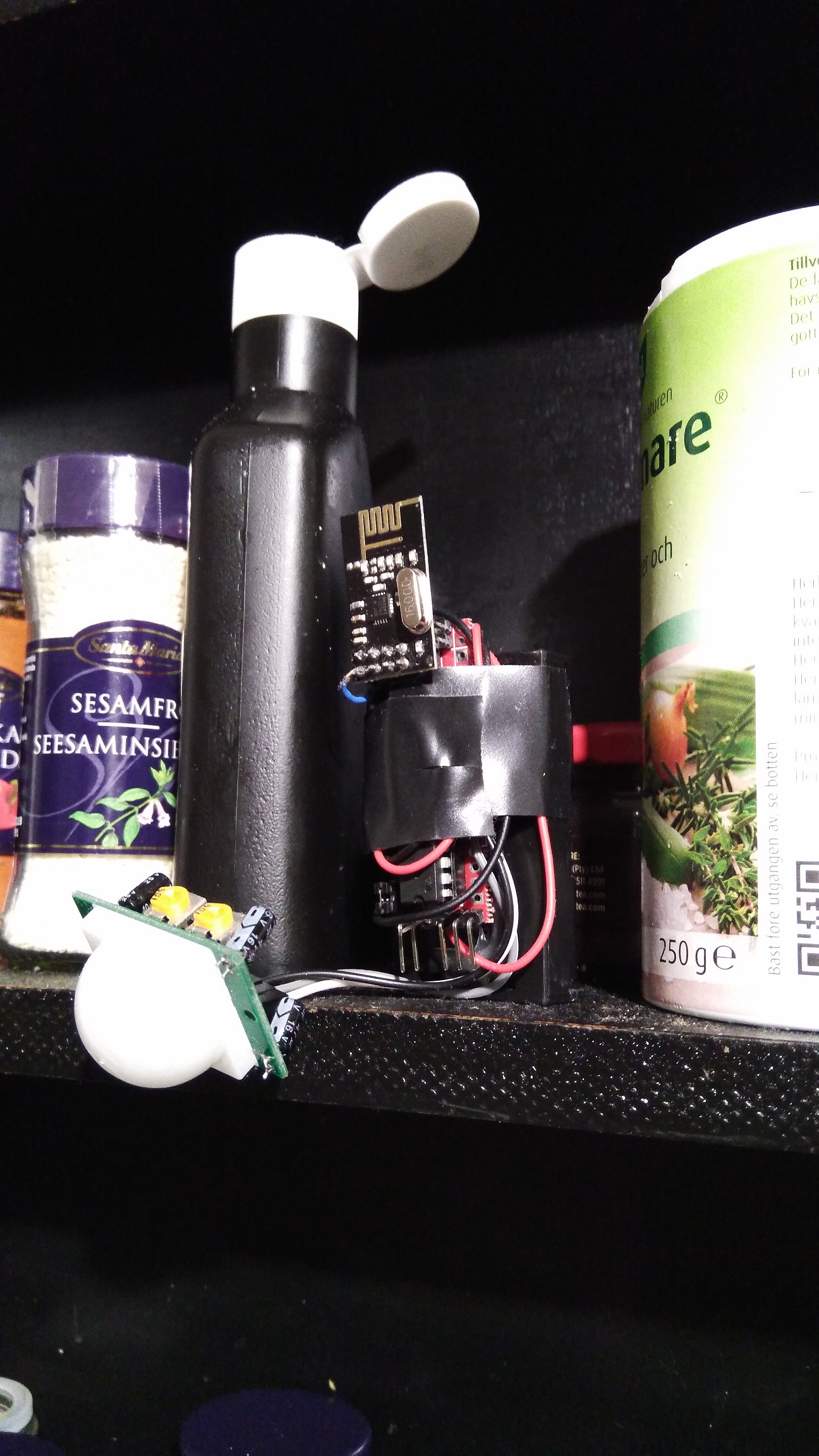
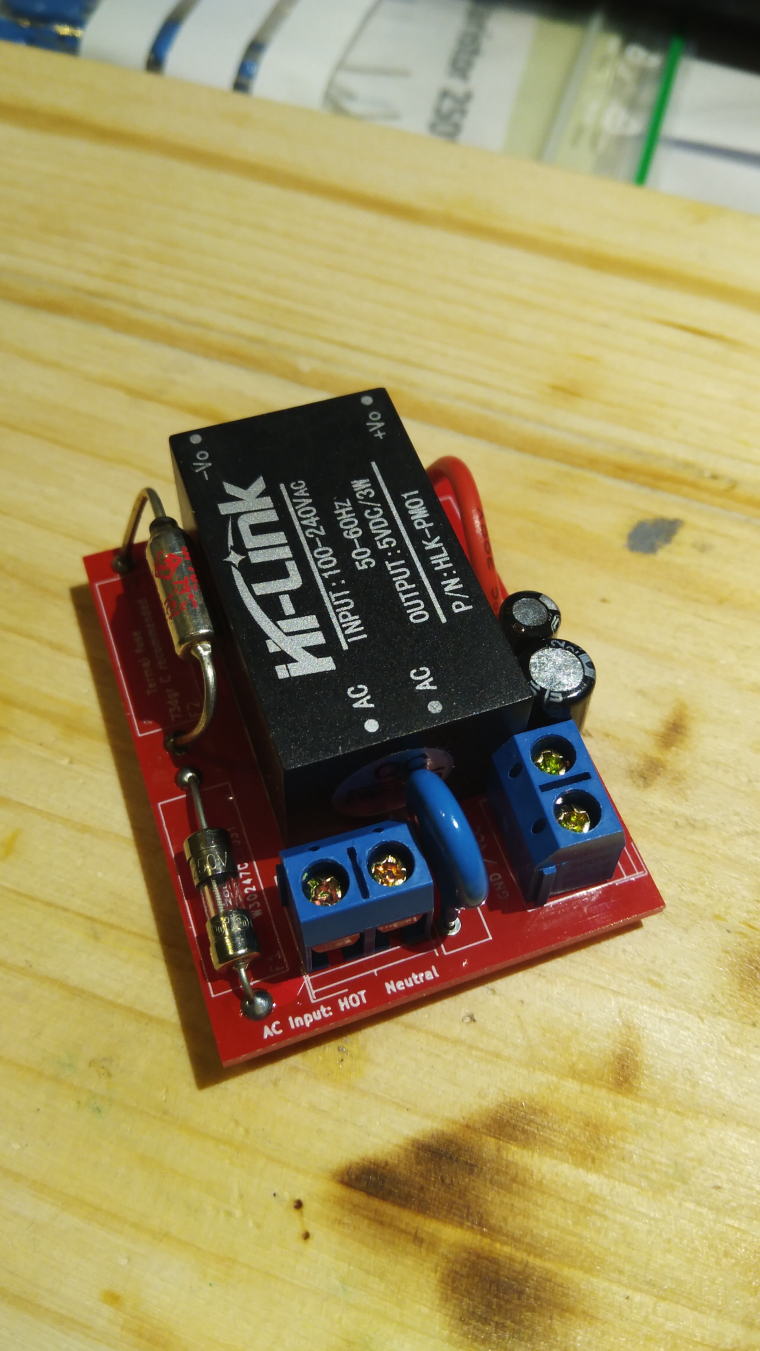
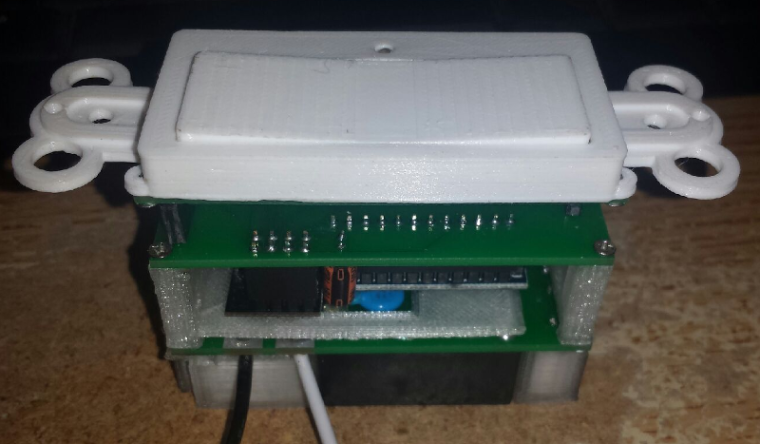
Finished assembling my HLK module...
-
Finished assembling my HLK module...
@sundberg84 Out of curiosity, How did you solder your thermal fuse on? What temperature thermal fuse did you use?
-
@sundberg84 Out of curiosity, How did you solder your thermal fuse on? What temperature thermal fuse did you use?
@dbemowsk 74dgr C and solder it as usual (but quick and make it go down in temp before solder again). No problem. I have longer legs so it can touch the HLK module and that might help.
-
@dbemowsk 74dgr C and solder it as usual (but quick and make it go down in temp before solder again). No problem. I have longer legs so it can touch the HLK module and that might help.
@sundberg84 the last few I did on my scene controller power supply boards I ended up using an ice pack on it while soldering. I had blown a good handful of these till I figured that out. I use similar 73°C fuses and keep the legs as long as I can and attach it to the side of the HLK case with a tiny dab of superglue.
-
Holding the leg with a big pair of pliers is, in my experience, a good way to keep the temperature down. Something like this can absorb a lot of heat:
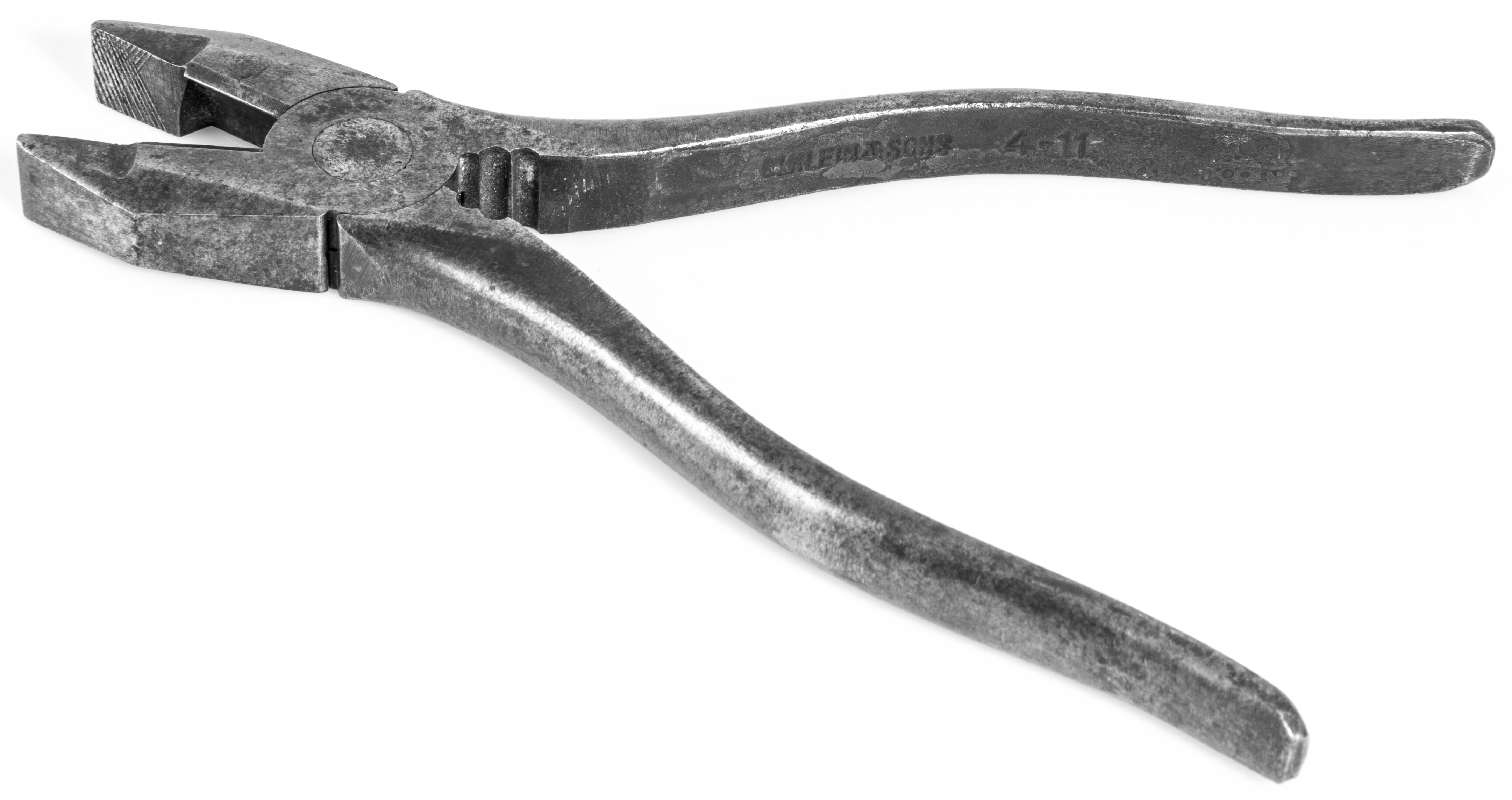
@mfalkvidd I would agree, but when space is cramped, those are not always a workable solution. Great suggestion though.
Vera Plus running UI7 with MySensors, Sonoffs and 1-Wire devices
Visit my website for more Bits, Bytes and Ramblings from me: http://dan.bemowski.info/ -
@mfalkvidd I would agree, but when space is cramped, those are not always a workable solution. Great suggestion though.
@dbemowsk true. But from the photo sundberg84 posted, there seems to be a lot of space so in his particular case it should work. Needle-nose pliers are also useful. They can't absorb as much heat, but they absorb some (especially if you put them in the freezer first ;-) ) and fit into tight spaces.
-
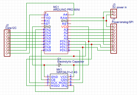
@dbemowsk said in What did you build today (Pictures) ?:
If anyone can see any problems or have any other suggestions for this design, let me know.
You had earlier lamented the low refresh rate. If you have the gumption, how about adding an SPI OLED interface such that it can do either I2C or SPI for the OLED? Having that extra option would only cost you at most 2.54mm in the vertical dimension.
@neverdie So because of your suggestion, I decided to explore the revision to the main controller board. I have not posted this revision to OpenHardware.io yet. Thought I'd get some feedback here first.
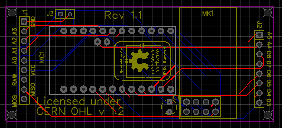
Some of the minor changes that I made were to the definitions of the headers. The headers now are labaled J1, J2 and J3. One other change was to combine the old J2 and J3 together into one header which is now designated J2. The biggest change was breaking out the MOSI and MISO SPI lines to the new J1 header. All changes are backward compatible with the old switch board hat. Here is the proposed board design. With the SPI bus now broken out, this will now allow the use of SPI capable displays and sensors such as the 128 x 64 OLED display for my current display/keypad board. I will make the changes to that soon.
The schematic is simple.
-
@neverdie So because of your suggestion, I decided to explore the revision to the main controller board. I have not posted this revision to OpenHardware.io yet. Thought I'd get some feedback here first.
Some of the minor changes that I made were to the definitions of the headers. The headers now are labaled J1, J2 and J3. One other change was to combine the old J2 and J3 together into one header which is now designated J2. The biggest change was breaking out the MOSI and MISO SPI lines to the new J1 header. All changes are backward compatible with the old switch board hat. Here is the proposed board design. With the SPI bus now broken out, this will now allow the use of SPI capable displays and sensors such as the 128 x 64 OLED display for my current display/keypad board. I will make the changes to that soon.
The schematic is simple.
-
@dbemowsk I thought they were all on the same board. I hadn't realized that they were separate boards. Also, at least on the schematic, the pinout on your pro-mini looks unusual.
@neverdie It was one that I found on EasyEDA that was contributed by a user. Some of the other ones didn't have A4 and A5 for I2C on them. All parts are correct on the board layout though which is what matters.
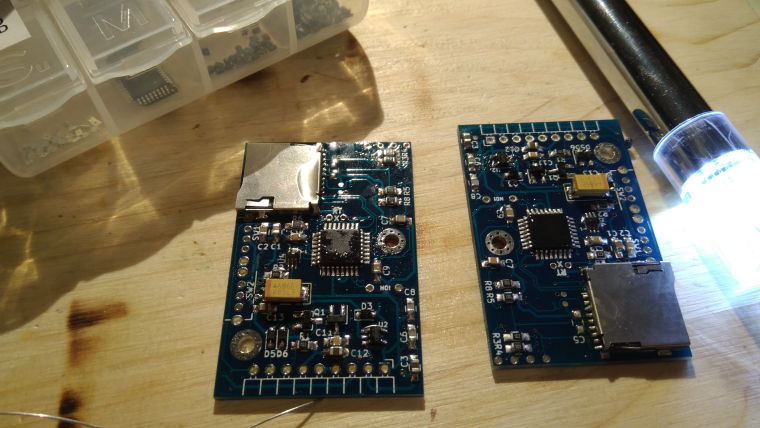
My setup for these is 3 boards. Power supply, controller and switch/sensor board with faceplate. This is how the 3 boards stack together.
This setup allows me to build different faceplate boards with various switches, displays and sensors depending on what the needs are.
-
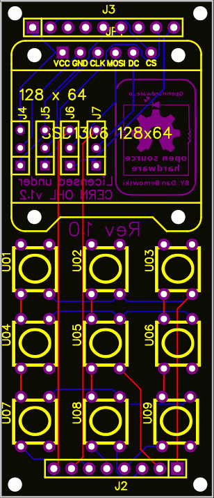
So here is an updated board layout that with the new controller board layout will allow for either a 6 pin SPI or 4 pin I2C OLED display. J4 through J7 are jumper headers that tell whether you are using a 6 pin SPI or 4 pin I2C display.
-
Building some loggers which i might sell later on.
-
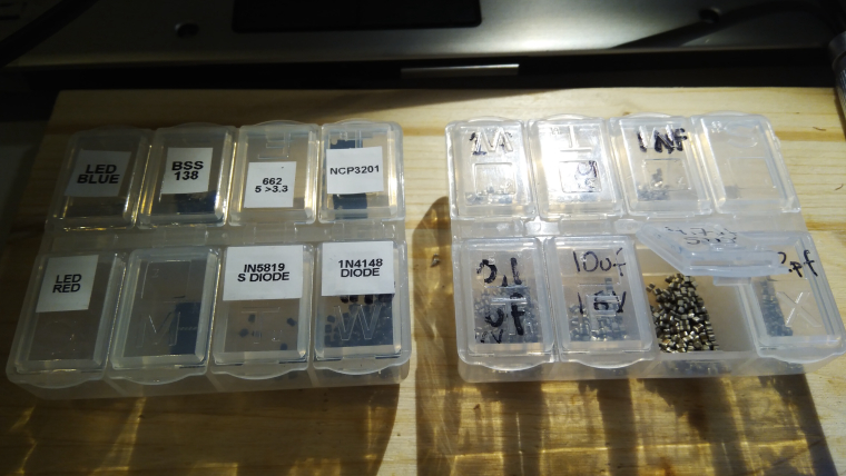
And want to make a tip about smd component organisation...
-
@neverdie I thought about adding jumpers, but being that these are in-wall switches which are pretty much permanent, and the fact that because of space the OLED display needs to be soldered in place, there's not much chance of the display getting changed from I2C to SPI or vice versa. I figured that the pads could just be bridged one way or the other depending on configuration.
-
And want to make a tip about smd component organisation...
@sundberg84 said in What did you build today (Pictures) ?:
And want to make a tip about smd component organisation...
I think we should make another topic for this kind of tips ? We could discuss pros and cons and give reference to online shops to buy items, your boxes are quite nice for DIP components and small breakout boards, where are they from ?
For SMDs components I went for the lab supplies on AliExpress, I started to sort my SMD chips using 5ml tubes and 3D printed holders, I need to print more holders to sort by categories as it's a bit messy at the moment. I put a bigger sticker on the side of tubes with more details as top sticker is pretty small :D Same holders can also holder bigger tubes for bigger stuff like here mini/micro USB plugs.
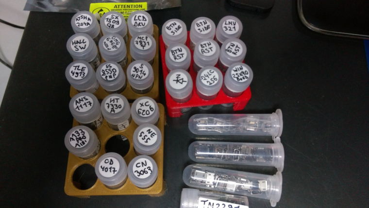
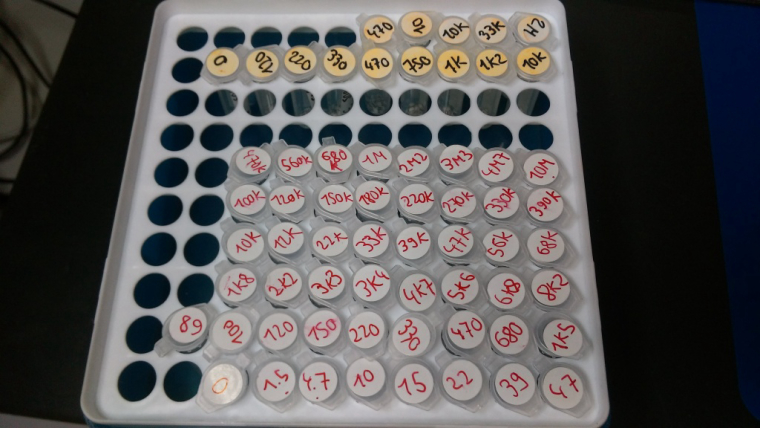
For resistors, capacitors, inductances, ... I went for lab tube boxes. I use smaller tubes (1.5 or 2ml) but they can hold probably thousands of 0603 or 0402 and even hundreds of the 0805 and 1206 resistors. I use different colors to differentiate size (and later precision/voltage/... when I'll have more boxes) and put bigger stickers on the lid of the box with information for each color.
-
Here, I like using smd books but of course I have a lot of these little boxes, too much though, and not enough!
Little boxes are nice but not very handy as you spend your time to reorganize them. Whereas I can have dedicated pages in books for my designs. Sure I could have dedicated boxes, but that takes more place and I don't have to search for a partvalue in hundreds of box. -
@sundberg84 said in What did you build today (Pictures) ?:
And want to make a tip about smd component organisation...
I think we should make another topic for this kind of tips ? We could discuss pros and cons and give reference to online shops to buy items, your boxes are quite nice for DIP components and small breakout boards, where are they from ?
For SMDs components I went for the lab supplies on AliExpress, I started to sort my SMD chips using 5ml tubes and 3D printed holders, I need to print more holders to sort by categories as it's a bit messy at the moment. I put a bigger sticker on the side of tubes with more details as top sticker is pretty small :D Same holders can also holder bigger tubes for bigger stuff like here mini/micro USB plugs.
For resistors, capacitors, inductances, ... I went for lab tube boxes. I use smaller tubes (1.5 or 2ml) but they can hold probably thousands of 0603 or 0402 and even hundreds of the 0805 and 1206 resistors. I use different colors to differentiate size (and later precision/voltage/... when I'll have more boxes) and put bigger stickers on the lid of the box with information for each color.
-
@neverdie I have plastic boxes from my local supermarket, I put components/breakout boards etc inside in their antistatic bags, then align them on their side in drawers. Less convenient to access but at least it's cleaned and ordered :)
Hello! It looks like you're interested in this conversation, but you don't have an account yet.
Getting fed up of having to scroll through the same posts each visit? When you register for an account, you'll always come back to exactly where you were before, and choose to be notified of new replies (either via email, or push notification). You'll also be able to save bookmarks and upvote posts to show your appreciation to other community members.
With your input, this post could be even better 💗
Register Login