Trying to design MySensors PCB / Fritzing
-
Hi,
So far all my MySensors projects have either been running on breadboards or stripboards with lots of wires going everywhere, while the design in most cases is the same. Some of the older sensors are a bit unreliable due to the jumper wires just making not good enough connections, etc. So I thought it would be interesting to design a PCB, something I have always wanted to do at some point, but now with PCB printing becoming more accessible (and cheaper) this actually becomes an option for me. I considered the EasyPCB too, but just think this might be a good skill to learn for some other projects in the future :smile:
So, I was trying to design a PCB in Fritzing - Also have tried KiCad but I think that is just a tiny bit next level, although the routing seems to be easier. However, got some issues with getting all the parts loaded properly (have the MySensors library loaded however) .
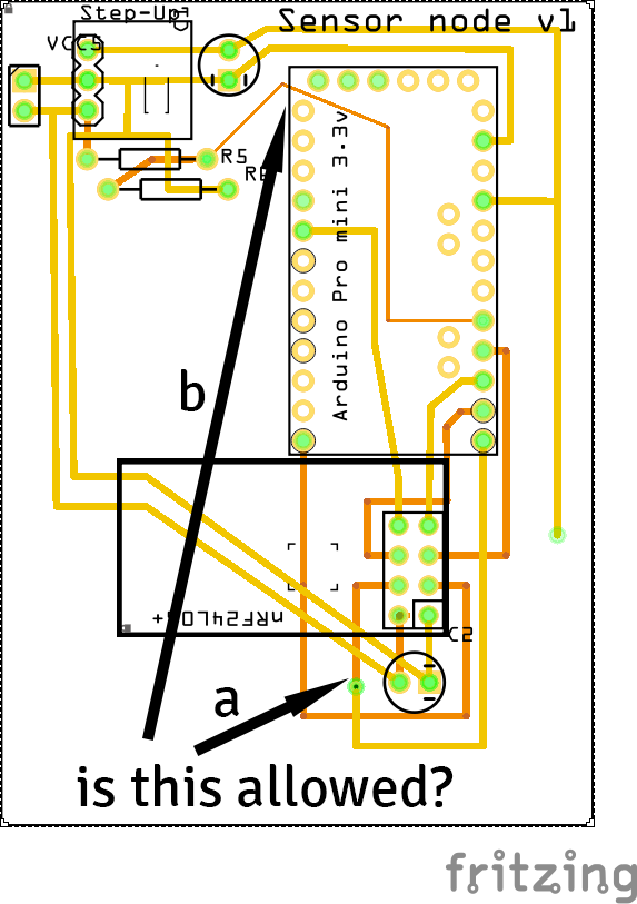
I did some reading and I was wondering if the following two things in the image are allowed?
A: Shows a "via" which makes a change from layer top/bottom to the other one to "cross" two other wires
B: Shows are trace (12mil) going between two holes of the Arduino. (this case the battery level check wire)Also:
- I assume for traces I do not need to stick to the grid.
- a different layer trace should not cross a hole, as that makes no sense and will become one when soldering.
It's a while new world and a lot of information everywhere, so I am just trying to stick to the basics of having wires not intersect with each other unless it's a VCC/GND
Thanks for your quick peek and feedback!
-
Hi,
So far all my MySensors projects have either been running on breadboards or stripboards with lots of wires going everywhere, while the design in most cases is the same. Some of the older sensors are a bit unreliable due to the jumper wires just making not good enough connections, etc. So I thought it would be interesting to design a PCB, something I have always wanted to do at some point, but now with PCB printing becoming more accessible (and cheaper) this actually becomes an option for me. I considered the EasyPCB too, but just think this might be a good skill to learn for some other projects in the future :smile:
So, I was trying to design a PCB in Fritzing - Also have tried KiCad but I think that is just a tiny bit next level, although the routing seems to be easier. However, got some issues with getting all the parts loaded properly (have the MySensors library loaded however) .
I did some reading and I was wondering if the following two things in the image are allowed?
A: Shows a "via" which makes a change from layer top/bottom to the other one to "cross" two other wires
B: Shows are trace (12mil) going between two holes of the Arduino. (this case the battery level check wire)Also:
- I assume for traces I do not need to stick to the grid.
- a different layer trace should not cross a hole, as that makes no sense and will become one when soldering.
It's a while new world and a lot of information everywhere, so I am just trying to stick to the basics of having wires not intersect with each other unless it's a VCC/GND
Thanks for your quick peek and feedback!
A) Yes, Vias is allowed - you will not be able to make more complex pcb witout vias. This is a common thing to do,
B) Yes, this is allowed - but its common to select a clearance/spacing in the pcb editor. This clearance should match atleast the minimum allowance from the pcb maker. Example from PCBway : Min manufacturable spacing is 4mil(0.1mm), strongly suggest to design spacing above 6mil(0.15mm) to save cost. There are then more to this when you reach a more advanced level with inductance, rf, high speed signals, power rails and so forth...
- No, you dont - but its quite neat to do so to keep things clean.
Im not sure if 2 was a question or not.
This looks very strange:
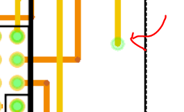
What I have read 90dgr turns on a trace doesn not decreace performance or makes any difference... but I have seen alot of comments not suggesting 90dgr turns on a trace.
I would recommend you not to have copper below the radio antenna. (Two traces)
Dont forget pinheaders or other measures to attach sensors.
If you are new to PCB design, youtube is your friend... there are alot of videos from beginner lever to advanced.
-
Hi!
I absolutely recommend that you invest the time needed to learn KiCad. Then you get all this stuff with clearances for free. You also get a whole library with footprints for components. KiCad will print originals for making the PCBs if you do that yourself.
You could also send the KiCad .pcb file to e.g. www.oshpark.com in the US. They charge $5 per sq. inch of 2-layer board and you get 3-boards for that price. They normally take one week to do the job and the result is excellent! -
A) Yes, Vias is allowed - you will not be able to make more complex pcb witout vias. This is a common thing to do,
B) Yes, this is allowed - but its common to select a clearance/spacing in the pcb editor. This clearance should match atleast the minimum allowance from the pcb maker. Example from PCBway : Min manufacturable spacing is 4mil(0.1mm), strongly suggest to design spacing above 6mil(0.15mm) to save cost. There are then more to this when you reach a more advanced level with inductance, rf, high speed signals, power rails and so forth...
- No, you dont - but its quite neat to do so to keep things clean.
Im not sure if 2 was a question or not.
This looks very strange:
What I have read 90dgr turns on a trace doesn not decreace performance or makes any difference... but I have seen alot of comments not suggesting 90dgr turns on a trace.
I would recommend you not to have copper below the radio antenna. (Two traces)
Dont forget pinheaders or other measures to attach sensors.
If you are new to PCB design, youtube is your friend... there are alot of videos from beginner lever to advanced.
Hi sundberg84,
Thanks for your reply!
The "lose trace" was more just a stopping point, as I wanted to be sure that I was doing things how they (kind of) should be! I thought it would not be good to try to make everything perfect, and then end up with question 1 being "no" :relaxed:.
All your other answers are clear, thanks a lot for that!
@bgunnarb: Thanks for the suggestion! I did run into issues where KiCad is a bit.. too much on the parts (eg. I should measure the dimensions of my resistors to find the right option in the list). I also ahd some issues with schemas / footprints (not every part has a footprint or a schema, such as the MySensors library). but I suppose I can just work with footprints.
Maybe I will give it another try. It does make a "cleaner" PCB when I was trying to make something similar as the image above.:slightly_smiling_face:
- No, you dont - but its quite neat to do so to keep things clean.
-
Hi sundberg84,
Thanks for your reply!
The "lose trace" was more just a stopping point, as I wanted to be sure that I was doing things how they (kind of) should be! I thought it would not be good to try to make everything perfect, and then end up with question 1 being "no" :relaxed:.
All your other answers are clear, thanks a lot for that!
@bgunnarb: Thanks for the suggestion! I did run into issues where KiCad is a bit.. too much on the parts (eg. I should measure the dimensions of my resistors to find the right option in the list). I also ahd some issues with schemas / footprints (not every part has a footprint or a schema, such as the MySensors library). but I suppose I can just work with footprints.
Maybe I will give it another try. It does make a "cleaner" PCB when I was trying to make something similar as the image above.:slightly_smiling_face:
@kokosnoot MySensors kicad library: https://github.com/mysensors-kicad
-
@kokosnoot MySensors kicad library: https://github.com/mysensors-kicad
@sundberg84 said in Trying to design MySensors PCB / Fritzing:
@kokosnoot MySensors kicad library: https://github.com/mysensors-kicad
I managed to install that one with a bit of effort last weekend. :ok_hand: :smiley:
However, inspired by bgunnarb I am already trying again for 40minutes to get a DHT11 footprint properly working, but failing thus far. There seems to be some in: https://github.com/KiCad/kicad-footprints/tree/master/Sensor.pretty but KiCad does not appreciate that as a library, (the default is to work from github.com/kicad/Capacitors_SMD.pretty for example, but those are all archived pages)
I manually tried adding https://github.com/KiCad/kicad-footprints/tree/master/Sensor.pretty - similar as the other libraries (type Github, etc) but just get a "ZIP error"... Maybe I should try a nightly build instead of the stable 5.0.2.
Edit: Just got it to work by downloading the entire 5.1.0 footprint library locally, and pointing to the [..]\footprints\Sensor.pretty file. Inspired by someone else with the same issue: https://forum.kicad.info/t/personal-footprints-via-on-demand-github-plugin-error-reading-zip-local-header/11777 :smiley:. Hopefully this info might help someone else at some point!
Hello! It looks like you're interested in this conversation, but you don't have an account yet.
Getting fed up of having to scroll through the same posts each visit? When you register for an account, you'll always come back to exactly where you were before, and choose to be notified of new replies (either via email, or push notification). You'll also be able to save bookmarks and upvote posts to show your appreciation to other community members.
With your input, this post could be even better 💗
Register Login